
Related Manuals for Panasonic SL-SX430EB


Summary of Contents for Panasonic SL-SX430EB
- Page 1 ORDER No.AD0402012C8 Portable CD Player SL-SX430EB / SL-SX430EG / SL-SX430GC / SL-SX430GK / SL -SX430GS Colours (S)....Silver Type (A)....Blue Type (EB, EG, GC areas) SPECIFICATIONS Specification...
- Page 2 Audio (CD-DA) Sampling frequency: 44.1 kHz No. of channels: 2 (left and right, stereo) Frequency response: 20 to 20,000 Hz / (+0dB to -7dB) Headphone output level: RMS max. 6mW+6mW/ 16 (adjustable) Pickup Light source: Semiconductor laser Wavelength: 780 nm Supported bit-rates: 32 kbps to 320 kbps / (128 kbps is recommended)
-
Page 3: Precaution Of Laser Diode
Specifications are subject to change without notice. Mss and dimensions are approximate. Note on CD-R and CD-RW: This unit can play CD-R and CD-RW recorded with CD-DA or MP3. Use an audio recording disc for CD-DA and finalize* it when you finish recording. - Page 4 1. Do not disassemble the optical pickup unit, since radiation from exposed laser diode is dangerous. 2. Do not adjust the variable resistor on the pickup unit. It was already adjusted. 3. Do not look at the focus lens using optical instruments. 4.
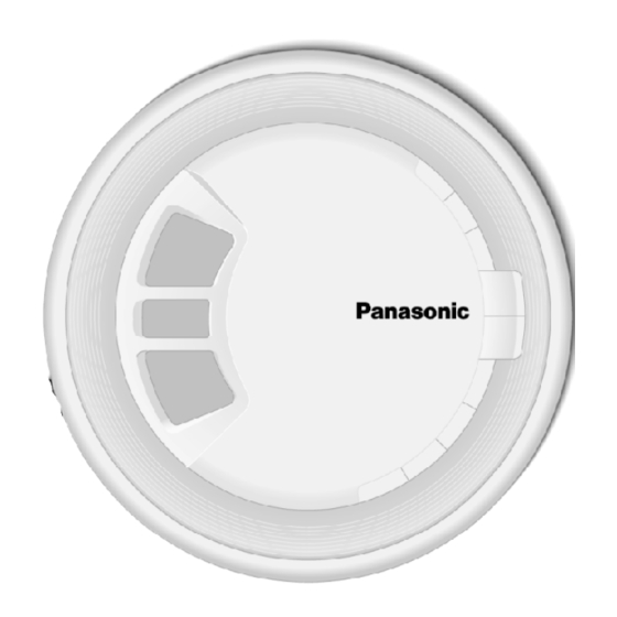
- Page 5 - AC adaptor...............1 pc. (RFEA435B-S) For (EG) area: - AC adaptor...............1 pc. (RFEA431E-S) For (GC) area: - AC adaptor...............1 pc. (N0JDCE000001) - Power plug adaptor..........1 pc. (K2DA42E00001) For (GK) area: - AC adaptor...............1 pc. (RFEA437T-S) 3. Location of controls / Connection to other equipment 4.
- Page 6 4.2. Caution when replacing traverse deck The new traverse deck short-circuits by the short pin, the foil (C) and short lands to protect the laser diode against electrostatic breakdown. Be sure to replace to new one following procedures. 1. Remove the short pin from the FFC, and then connect it to the connector.
-
Page 7: Operation Checks And Component Replacement Procedures
the wrist strap. So, take care not to let your clothes touch the traverse deck (optical pickup). Fig. 2 Fig. 3 5. Operation Checks and Component Replacement Procedures - This section describes procedures for checking the operation of the major printed circuit boards and replacing the main components. - Page 9 - Check the P.C.B. ass’y (A side) as shown below.
- Page 10 5.1.2. Checking for the P.C.B. ass’y / (B side) - Follow the (Step1)-(Step6) of item 5.1.1. - Check the P.C.B. ass’y (B side) as shown below.
- Page 11 5.2. Replacement for the CD lid unit - Follow the (Step1)-(Step4) of item 5.1.1.
- Page 12 5.3. Replacement for the LCD, operation button, LCD panel and multi button SW unit - Follow the (Step1)-(Step4) of item 5.1.1. - Follow the (Step1)-(Step4) of item 5.2.
- Page 13 5.4. Replacement for the spring retainer plate and open spring - Follow the (Step1)-(Step4) of item 5.1.1. - Follow the (Step1)-(Step4) of item 5.2.
- Page 14 5.5. Replacement for the traverse motor - Follow the (Step1)-(Step3) of item 5.1.1. NOTE: Be sure to confirm the item 4 “Handling Precautions for Traverse Deck” before removing the traverse deck unit.
- Page 15 5.6. Replacement for the optical pick-up - Follow the (Step1)-(Step3) of item 5.1.1. - Follow the (Step1)-(Step3) of item 5.5.
- Page 17 5.7. Replacement for the rest switch - Follow the (Step1)-(Step3) of item 5.1.1. - Follow the (Step1), (Step2) of item 5.5.
- Page 18 6. Checking the Operation Problems on the Traverse...
- Page 19 Deck (Optical Pickup) Make sure to follow the procedures below to check the operation problems of the traverse deck (optical pickup) before replacing it. Replace the traverse deck only after the problem is identified. Check the operations described below on the traverse deck after replacing it. *Checking Skip Search 1.
-
Page 20: Automatic Adjustment Results Display Function (Self-Check Function)
and reverse directions). *Checking Playability 1. Play the 0.7 mm black dot and the 0.7 mm wedge on the playability test disc (SZZP1054C) and verify that no sound skip or noise occurs. 2. Play the middle tracks of the uneven test disc (SZZP1056C) and verify that no sound skip or noise occurs. - Page 21 <Example> Follow the below steps when “E-1” is displayed. (Cause: Focus balance (FBC) is set beyond the limit.) Check if 1. the waveform or voltage of the focus servo circuit is correct. (check the waveform or voltage.) 2. the optical pickup returns to the normal state by exchanging the traverse deck.
-
Page 22: Display Of Self-Diagnostic Function
2. the waveform or voltage of the servo IC’s are correct. (check the waveform or voltage.) Note: It is not always necessary to exchange the traverse deck when an error message is displayed. Be sure to check if the circuit is defective or not before exchanging the traverse deck. Note: If any other disc than the test disc (SZZP1054C) is used, an error message may be displayed. - Page 23 S821: Memory/ Recall/ AB repeat/ Digital Re-master/ Anti-skip mode selection (MEMO) switch. S822: Play mode selection (MODE) switch. S823: Sound quality selection (EQ) switch. S824: Play/pause ( ) switch. S825: Stop/Turn off ( ) switch. S826, 827: Skip/search ( ) switch. S828, 829: Volume control (VOL+,VOL -) switch.
- Page 24 valuesandwaveformsdepending upon the internal impedance of the tester or measuring unit. Measurement conditions: *( )..CD playback mode (Test disc 1kHz, L+R, 0dB) *No mark..CD stop mode Caution!! - IC and LSI are sensitive to static electricity. - Secondary trouble can be prevented by taking care during repair. - Cover the parts boxes made of plastics with aluminum foil.
- Page 25 Function Terminal Name APC amplifier input terminal Laser power drive signal output Power supply terminal EQSW EQ characteristic drive signal input RFOUT Not used, open RF IN RF signal input terminal CAGC AGC loop filter capacity connection terminal RF signal output terminal H.P.F.
- Page 26 Focus signal input terminal Function Terminal Name RF addition amplifier input terminal Focus signal input terminal 32 SHARP= LD reference voltage input terminal 14.2. IC301(C2BBGE000730): / System Control / LCD Drive Function Terminal Name 6KEY 6Key Remote control key signal input 2 DOCTOR Doctor mode select signal input...
- Page 27 Function Terminal Name Not used, open 24 TYPESEL2 I Model selection input 25 /RESET Reset detect signal input 26 EXT-IN Oscillator connected terminal (F= 32.7 kHz) EXT- 28 XOSCIN System clock signal 29 XOSCOUT O REST Rest detect switch signal input 32 A.SHOCK Not used, open HOLD...
- Page 28 Function Terminal Name Power supply terminal VREF Reference voltage input terminal COM3 LCD common signal output terminal COM0 Power supply terminal Power supply terminal (LCD drive bias) Power supply terminal (LCD drive bias) 14.3. IC501(MN6627935CJ): / Servo Processor/ Digital Signal Processor/ Digital Filter &...
- Page 29 Terminal Function Name Power supply terminal SPOUT O Spindle motor drive output terminal SPPOL O Spindle motor drive output terminal TRVP O Traverse drive (+) output terminal TRVM O Traverse drive (-) output terminal IPFLAG2/ Not used, open SRDATA REGON Not used, connected to GND O Tracking coil drive (+) output terminal...
- Page 30 Terminal Function Name PWMSEL PWM output mode select signal PLLF O PLL loop filter PLLFO O PLL loop filter LOOUTL Not used, open LOOUTR Not used, open Power supply terminal HPCNT Headphone output control signal HPOUTR O R ch for headphone signal output Power supply terminal HPOUTL...
-
Page 31: Replacement Parts List
*When replacing any of components, be sure to use only manufactures specified parts shown in the parts list. *The parenthesized indications in the Remarks columns specify the product. / (EBA): SL-SX430EB -A / (EBS): SL-SX430EB-S / (EGA): SL-SX430EG-A / (EGS): SL-SX430EG-S / (GCA): SL-SX430GC-A / (GCS): SL-SX430GC-S / (GKS): SL-SX430GK-S / (GSS):SL-SX430GS-S Parts without these indications can be used for all products. - Page 32 Ref. No. Part No. Part Name & Description Remarks RAE0241Z-M TRAVERSE DECK UNIT RMG0605-K1 FLOATING RUBBER RAF0241A OPTICAL PICK-UP RDG0554 GEAR 1 RDG0555 GEAR 2 RMQ1125-1 MOTOR HOLDER RMS0782 SHAFT XQN17+BG45 SCREW RXQ0971-3 MOTOR ASS’Y RGV0200-H1 KNOB,HOLD RJC93038-3 BATTERY TERMINAL RKS0392-A BOTTOM CABINET RMC0585...
- Page 33 Ref. No. Part No. Part Name & Description Remarks RQT7186-E O/I BOOK (EGA)(EGS) English / French / Spanish / Netherlands Danish / Italian / Portuguese Russian / Czeco / K2DA42E00001 POWER PLUG ADAPTOR (GCA)(GCS) N0JDCE000001 AC ADAPTOR (GCA)(GCS) RQT7637-K O/I BOOK (GCA)(GCS)(GSS)( Chinese RQT7638-A...
- Page 34 Ref. No. Part No. Part Name & Description Remarks C509 ECJ1VB1C104K 16V 0.1U C510 ECJ1VF1C104Z 16V 0.1U C511 ECJ1VB1C104K 16V 0.1U C513 ECJ1VF1C104Z 16V 0.1U C517 ECJ1VF1A105Z 10V 1U C518 ECJ1VC1H101K 50V 100 C527,28 ECJ1VF1C104Z 16V 0.1U C530 ECUV1H330GCV 50V 33P ECJ1VC1H330G C611 ECJ1VF1C104Z...
- Page 35 RPF0111-2 PROTECTION BAG (EGA)(EGS)(GCA)(...
- Page 36 Ref. No. Part No. Part Name & Description Remarks RPK2131 GIFT BOX (GCA)(EGA) RPQ1663 (EGA)(EGS)(GKS)( RPQ1644 (GCA)(GCS) RPK2144 GIFT BOX (GKS) RPK2081 GIFT BOX (EGS)(GCS)(GSS) RPQ1710 SHEET 2 (EBS) PCB1 REP3681B-M P.C.B. ASS’Y [RTL] 2SB1182TLPQR TRANSISTOR B1BDND000001 B1ABMD000004 TRANSISTOR UNR521L00L TRANSISTOR UNR511400L TRANSISTOR...
-
Page 37: Cabinet Parts Location
Ref. No. Part No. Part Name & Description Remarks R302 ERJ3GEYJ104 1/10W 100K R304 ERJ3GEYJ105V 1/10W 1M R305 ERJ3GEYJ335V 1/10W 3.3M R306 EXBV8V473JV 1/16W 47K R307 ERJ3GEYJ103V 1/10W 10K D0GB103JA002 R308 ERJ3GEYJ104 1/10W 100K R309 EXBV8VR000V 1/8W 0 R311 ERJ3GEYJ102V 1/10W 1K R313 EXBV8V104JV... - Page 38 17. Traverse Parts Location...
- Page 39 18. Packaging 18.1. SL-SX430EB...
- Page 40 18.2. SL-SX430EG / SL-SX430GK / SL-SX430GS...
- Page 41 18.3. SL-SX430GC...
-
Page 42: Schematic Diagram For Printing With Letter Size
19. Schematic Diagram for printing with letter size K0402 YH/HM... - Page 43 :POSITIVE VOLTAGE LINE :PLAYBACK SIGNAL LINE OPERATION & LCD UNIT LCD801(L5ACAFC00004) LCD DISPLAY R828 R827 R826 R825 R824 R823 20.5K 6.8K 5.6K 20.5K 6.8K 5.6K R822 A B C D E F G H I J K L M N O P Q R T U V W R821 VREF...
- Page 44 :POSITIVE VOLTAGE LINE :PLAYBACK SIGNAL LINE 2.7V 1.5V 3.2V 36 35 34 33 32 31 30 29 28 27 26 25 1.7V 0V (0.2V) SOFT SPRT C513 2.7V RESET1 RESET2 IC11 OFF/START TRV- C0DBFFB00004 CD/TU TRV+ 0.9V (0.7V) POWER SUPPLY/ SPOUT 2200P MOTOR DRIVE...
- Page 45 :POSITIVE VOLTAGE LINE :PLAYBACK SIGNAL LINE 2.7V MA111TX UN5215TX DC IN DET. (BATTERIES) ICP11 ERBFE1R50U CN11 2.9V 2 R6/LR6(UM-3) 2SB1182TLPQR BATTERIES REGULATOR 2.9V 5.3V JK11 DC IN 4.5V 2.7V 2.7V UN5213TX RESET 2.7V Q301 2.7V UN5213TX RESET UN5113TX 2.7V RESET 2.7V UN521LTX DC IN DET.
- Page 46 C0CBAAB00043 2SB1182TLPQR C0DBFFB00004 48PIN C2BBGE000730 80PIN AN22003A-NF 32PIN MN6627935CJ 100PIN C3ABMG000103 50PIN C3EBCG000096 8PIN No.1 No.1 B1ABMD000004 B1GFGCAA0001 MA111TX 2SK1958T1 B1CHMC000001 UN5113TX UN5215TX B1CHGD000004 Cathode UN5213TX UN521LTX UN5114TX UNR521000L UN5214TX 2SB709ATX Anode MA8056MTX Cathode Anode...
- Page 48 AN22003A-NF VREF IC101 SERVO AMP MN6627935CJ OPTICAL PICK-UP IC501 SERVO PROCESSOR / DIGITAL SIGNAL PROCESSOR DIGITAL FILTER & D/A CONVERTER 3TOUT RFENV 3TENV OFTR OFTR OFTR +B3 +B5 Q201 AGC RFEQ LASER POWER DRIVE RF AMP NRFDET NRFDET DET. FE IN SUBT DIGITAL OUT SEMICONDUCTOR...
- Page 49 HEADPHONE DC IN 4.5V DC IN DET. Q704 MUTING Q901,902,905 REGULATOR MUTING CONT. Q903 ICP11 BUZZER RESET RESET CONT. LCD801 Q301 LCD DISPLAY RESET Q904 2 R6/LR6(UM-3) BATTERIES POWER SUPPLY C3EBCG000096 Q12~14 IC302 Q502 CHARGE EE PROM CONT. SWITCH- POWER SUPPLY POWER SUPPLY...
- Page 50 Note: This printed circuit board diagram may be modified at any time with the development of new technology. (SIDE : B) (SIDE : A) OPTICAL PICK-UP R122 R120 R101 C107 R107 R103 VREF C104 R102 R104 C121 Q101 C201 C108 R110 IC101 R501...
- Page 51 :POSITIVE VOLTAGE LINE :PLAYBACK SIGNAL LINE OPERATION VREF C111 0.022 PLAY PLAY IC101 PLAY 0.3V 70mV 0.7V AN22003A-NF SERVO AMP 2ms. 0.1V/DIV. 2ms. 20mV/DIV. s. 0.5V/DIV. R103 C121 C112 C117 560P 560P 0.022 R104 Q101 C116 UN5113TX 0.022 SWITCHING 1.3V 2.7V 2.7V OPTICAL PICK-UP...
- Page 52 OPERATION & LCD UNIT LCD801(L5ACAFC00004) LCD DISPLAY R828 R827 R826 R825 R824 R823 20.5K 6.8K 5.6K 20.5K 6.8K 5.6K R822 A B C D E F G H I J K L M N O P Q R T U V W R821 S824 B C D E...
- Page 53 :POSITIVE VOLTAGE LINE :PLAYBACK SIGNAL LINE 2.7V 1.5V 3.2V C513 0V(1.6V) BA1/LRCK (2.2V)0V 0V(1.6V) 1.5V 3.2V (0.7V) 0V(1.5V) SPOUT 0V(1.5V) SPPOL 3.2V(1.5V) TRVP 0V(1.5V) TRVM 0V(1.5V) RJ503 IPFLAG2/SRDATA 3.2V(1.6V) REGON IC501 0V(1.5V) X501 R507 (16.9344MHz) MN6627935CJ 0V(1.5V) SERVO PROCESSOR/ 0V(1.5V) DIGITAL SIGNAL PROCESSOR/ (0.2V) 0V(1.5V)
- Page 54 36 35 34 33 32 31 30 29 28 27 26 25 1.7V 0V (0.2V) SOFT SPRT 2.7V RESET1 RESET2 IC11 OFF/START TRV- C0DBFFB00004 CD/TU TRV+ 0.9V (0.7V) POWER SUPPLY/ SPOUT 2200P MOTOR DRIVE 0.6V SPPOL CRIP 1.3V CHARGE 270P 2.9V PVcc1 2.7V...
- Page 55 :POSITIVE VOLTAGE LINE :PLAYBACK SIGNAL LINE 2.7V MA111TX UN5215TX DC IN DET. (BATTERIES) ICP11 ERBFE1R50U CN11 2.9V 2SB1182TLPQR REGULATOR 2.9V 5.3V 2.7V 2.7V UN5213TX RESET 2.7V Q301 2.7V UN5213TX RESET UN5113TX 2.7V RESET 2.7V UN521LTX DC IN DET. (AC ADAPTOR) UN5114TX CHARGE CONT.
- Page 56 MA111TX ICP11 ERBFE1R50U CN11 2 R6/LR6(UM-3) BATTERIES 2.9V JK11 DC IN 4.5V BMD000004 GE CONT. 2.7V L903 L902 JK702 HEADPHONE L905 EG,GC,GK,GS) CIRCUIT DIAGRAM...
Need help?
Do you have a question about the SL-SX430EB and is the answer not in the manual?
Questions and answers