Advertisement
Table of Contents
Advertisement
Table of Contents

Related Manuals for Casio EV-680


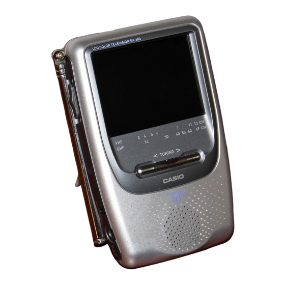
Summary of Contents for Casio EV-680
- Page 1 BLOCK DIAGRAM — 2 —...
- Page 2 ADJUSTMENT Items To Be Adjusted 1. VCC2 adjustment ,VCC7, VCC6, VCC5 & Vee1 voltage check 2. LLD Coil adjustment 3. Free running frequency adjustment 4. Bright, Sub-bright adjustment 5. Contrast, bright adjustment 6. VOM AC adjustment 7. VCOM DC coarse adjustment 8.
-
Page 3: Printed Circuit Boards
PRINTED CIRCUIT BOARDS K671B-DP PCB K671B-TU PCB TOP VIEW — 9 —... -
Page 4: Bottom View
K671B-DP PCB K671B-TU PCB BOTTOM VIEW — 10 —... - Page 5 DISASSEMBLY 1. Remove the screw and the antenna. Screw 2. Remove the stand and the battery cover. 3. Remove four screws and separate the side panel and the knob. Side panel Screws — 11 —...
- Page 6 4. Remove the connector and separate the LCD Assy. Connectors 5. Remove the screw, unsolder two speaker lines (grey and orange) and then separate the PCB Assy. Screw orange grey 6. Remove the tune button and separate the tuner cover. Remove four screws and separate the upper cover while paying attention to the hook.
- Page 7 7. Remove the hook, unsolder the fluorescent lamp and the LCD case and then separate the LCD Assy. Hooks 8. Remove the hook and disassemble the LCD Assy. Hooks Hooks — 13 —...
-
Page 8: Exploded View
EXPLODED VIEW ×2 — 14 —... - Page 9 SCHEMATIC DIAGRAMS DISPLAY PCB (K671B-DP) Display Controller Circuit Chroma Circuit To LCD Speaker Earphone Jack Audio Amplifier Circuit A/V Jack DC In To K671BR-TU PCB Display Generator Voltage Circuit — 16 —...
- Page 10 TUNNER PCB (K671B-TU) IF Detection Circuit Antenna Back Light IF Pad Power switch Power Supply Circuit 27.0 ~ 32.0. V 11.0 ~ 13.0 V 7.0 ~ 8.0 V 5.00 ± 0.02 V –16.0 ~ –14.0 V To K671BR-DP PCB — 17 —...
Need help?
Do you have a question about the EV-680 and is the answer not in the manual?
Questions and answers