Table of Contents
Advertisement
Quick Links
SERVICE MANUAL
Sec. 1: Main Section
I Specifications
I Preparation for Servicing
I Adjustment Procedures
I Schematic Diagrams
I CBA's
6719DC/
SSC719C
Sec. 2: Deck Mechanism Section
I Standard Maintenance
I Alignment for Mechanism
I Disassembly/Assembly of Mechanism
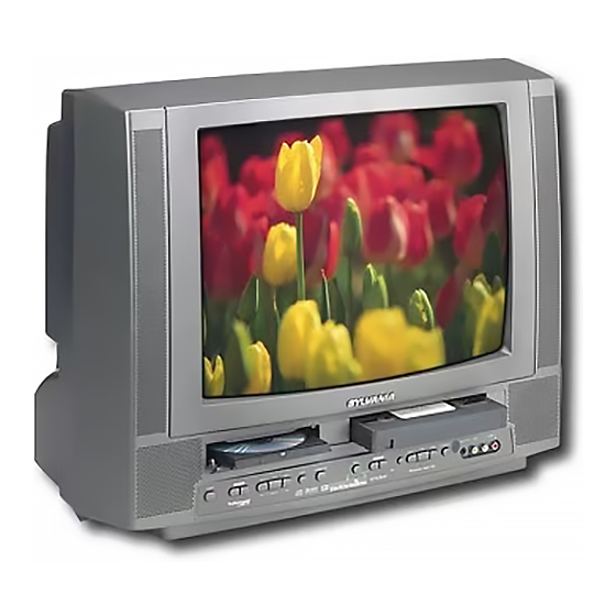
19" COLOR TV/DVD/VCR
Sec. 3: Exploded views
and Parts List Section
I Exploded views
I Parts List
EWC19T2
Advertisement
Chapters
Table of Contents

Subscribe to Our Youtube Channel
Related Manuals for Sylvania Emerson 6719DC


Summary of Contents for Sylvania Emerson 6719DC
- Page 1 SERVICE MANUAL Sec. 2: Deck Mechanism Section Sec. 3: Exploded views Sec. 1: Main Section I Standard Maintenance and Parts List Section I Specifications I Preparation for Servicing I Alignment for Mechanism I Exploded views I Disassembly/Assembly of Mechanism I Parts List I Adjustment Procedures I Schematic Diagrams I CBA’s...
- Page 2 IMPORTANT SAFETY NOTICE Proper service and repair is important to the safe, reliable operation of all Funai Equipment. The service procedures recommended by Funai and described in this service manual are effective methods of performing service operations. Some of these service special tools should be used when and as recommended.
-
Page 3: Table Of Contents
MAIN SECTION 19" COLOR TV/DVD/VCR 6719DC/SSC719C/EWC19T2 Sec. 1: Main Section I Specifications I Preparation for Servicing I Adjustment Procedures I Schematic Diagrams I CBA’s TABLE OF CONTENTS Specifications................1-1-1 Laser Beam Safety Precautions . -
Page 4: Specifications
SPECIFICATIONS *ˆ M ode---------SP mode unless otherwise specified *Test input terminal <Except Tuner>-------------Video input (1Vp-p) Audio input (-10dB) <Tuner>-----------------------Ant. input (80dBµV) Video: 87.5% Audio: 25kHz dev (1kHz Sin) <DEFLECTION> Description Condition Unit Nominal Limit 1. Over Scan — — Horizontal —... - Page 5 <VCR> Description Condition Unit Nominal Limit 1. Horizontal Resolution (R/P, SP) Line µS 2. Jitter (Low) (R/P, SP) 3. S/N Chroma AM(SP) (R/P, SP) PM(SP) (R/P, SP) 4. Wow & Flutter (JIS, UNWTD) (R/P, SP) 0.25 <TUNER> Description Condition Unit Nominal Limit 1.
-
Page 6: Laser Beam Safety Precautions
LASER BEAM SAFETY PRECAUTIONS This DVD player uses a pickup that emits a laser beam. Do not look directly at the laser beam coming from the pickup or allow it to strike against your skin. The laser beam is emitted from the location shown in the figure. When checking the laser diode, be sure to keep your eyes at least 30cm away from the pickup lens when the diode is turned on. -
Page 7: Important Safety Precautions
IMPORTANT SAFETY PRECAUTIONS Prior to shipment from the factory, our products are strictly inspected for recognized product safety and electrical codes of the countries in which they are to be sold. However, in order to maintain such compliance, it is equally important to implement the following precautions when a set is being serviced. - Page 8 ing is performed that involves B+, horizontal de- earth ground. If a voltage reading in excess of 1.0V flection or high voltage. Correct operation of the is obtained, remove and reinsert the AC power X-radiation protection circuits also must be recon- plug in the opposite polarity and again measure firmed each time they are serviced.
- Page 9 Precautions during Servicing H. When a power cord has been replaced, check that 5~6 kg of force in any direction will not loosen it. A. Parts identified by the ( # ) symbol are critical for I. Also check areas surrounding repaired locations. safety.
- Page 10 Safety Check after Servicing Examine the area surrounding the repaired location Chassis or Secondary Conductor for damage or deterioration. Observe that screws, parts and wires have been returned to original posi- tions. Afterwards, perform the following tests and con- Primary Circuit Terminals firm the specified values in order to verify compliance with safety standards.
-
Page 11: Standard Notes For Servicing
STANDARD NOTES FOR SERVICING Circuit Board Indications How to Read the Values of the Rect- angular Type Chip Components 1. The output pin of the 3 pin Regulator ICs is indi- cated as shown: Example: (a) Resistor Top View Bottom View Input = 473 = 47 [kΩ] (Top View) - Page 12 Notes: 2. The Flat Pack-IC on the CBA is affixed with glue, so be careful not to break or damage the foil of a. Do not attempt to lift the component off the board each pin or solder lands under the IC when remov- until the component is completely disconnected ing it.
- Page 13 Hot Air Blower Iron Wire Soldering Iron Fig. S-1-1 To Solid Mounting Point Fig. S-1-5 Hot-air Flat Pack-IC Desoldering Machine Example : Masking Flat Pack-IC Tape Tweezers Pin 1 of the Flat Pack-IC Fig. S-1-2 is indicated by a " "...
- Page 14 Instructions for Handling Semiconductors Electrostatic breakdown of the semiconductors may occur due to a potential difference caused by electro- static charge during unpacking or repair work. Ground for Human Body Be sure to wear a grounding band (1MΩ) that is prop- erly grounded to remove any static electricity that may be charged on the body.
-
Page 15: Preparation For Servicing
PREPARATION FOR SERVICING How to Enter the Service Mode Adjustment Mode No need to use. Caution: 1 Purity check mode: Shows Red, 1. Optical sensors system are used for Tape Start Green, Blue or White cyclically on the and End Sensor on this equipment. Read this page screen each time the “7”... -
Page 16: Operating Controls And Functions
OPERATING CONTROLS AND FUNCTIONS - TV/DVD/VCR FRONT PANEL - DVD buttons TV/VCR buttons F.FWD STOP/EJECT POWER PLAY VOLUME PLAY OPEN/CLOSE SELECT REC/OTR SKIP SKIP STOP CHANNEL HEADPHONE VIDEO AUDIO TV/VCR SEARCH 11 12 13 - REMOTE CONTROL - SELECT button Press to change to TV/VCR mode or DVD mode. - Page 17 - TV/DVD/VCR REAR PANEL - ANT. AUDIO OUT COAXIAL 48 49 Number buttons REPEAT button TV Mode: Repeats playback of the current disc, title, chapter Press two digits to directly access the desired or track. channel. ANGLE button (DVD mode) Remember to press a "0"...
-
Page 18: Cabinet Disassembly Instructions
CABINET DISASSEMBLY INSTRUCTIONS 1. Disassembly Flowchart REMOVAL This flowchart indicates the disassembly steps for the REMOVE/ LOC. PART cabinet parts, and the CBA in order to gain access to *UNHOOK/UNLOCK/ Fig. Note item(s) to be serviced. When reassembling, follow the RELEASE/UNPLUG/ steps in reverse order. - Page 19 Reference Notes in the Table Caution ! When removing the CRT, be sure to discharge the Anode Lead of the CRT with the CRT Ground Wire before removing the Anode Cap. Reference Notes in the Table CAUTION 1: Discharge the Anode Lead of the CRT with the CRT Ground Wire before removing the Anode Cap.
- Page 20 [1] REAR CABINET ANT. Fig. 1 [1] REAR CABINET Fig. 2 1-7-3 TD500DC...
- Page 21 [5] Shield Box [3] Tray Chassis [8] Filter [6] DVD Mechanism S-10 S-10 [11] Deck H.V. CBA [9] Bottom Assembly Plate S-10 S-12 [10] Power Supply/ [2] H.V. CBA AV CBA (wih Holder) S-11 [12] Main CBA S-11 Fig. 3 1-7-4 TD500DC...
- Page 22 Anode Cap CRT CBA [4] CRT Fig. 4 Short the three short lands by soldering CN101 [7] DVD Main CBA Unit CN401 View for A Short the three short lands by soldering DVD Mechanism Slide Pickup Unit View for C View for B Fig.
- Page 23 DVD MAIN CBA CRT CBA ANODE CN501 FACTORY USE ONLY CL501 SCREEN FOCUS CN501 CN701 CL504A CN403 CN404 FILTER CBA CN402 CN401 SPEAKER CN2801 CN2401 CN2402 CN2601 POWER SUPPLY/ AV CBA CN2602 CN2803 CN2804 CN2802 CN1805 CN1804 CN1803 CL1403 CL1401 MAIN CBA CN1303 INT MON...
-
Page 24: Electrical Adjustment Instructions
ELECTRICAL ADJUSTMENT INSTRUCTIONS General Note: How to Set up the Service mode: "CBA" is abbreviation for "Circuit Board Service Mode: Assembly." 1. Use the service remote control unit. 2. Turn the power on. (Use main power on the TV NOTE: unit.) Electrical adjustments are required after replacing 3. - Page 25 2. Auto AFT (VCO) Adjustment 4-1. H Adjustment Purpose: To operate AFT correctly. Purpose: To get correct horizontal position and size of screen image. Symptom of Misadjustment: AFT does not work cor- rectly and/or synchronization is faulty. Symptom of Misadjustment: Horizontal position and size of screen image may not be properly displayed.
- Page 26 4-2. C-Trap Adjustment 5. V. Size Adjustment Purpose: To get minimum leakage of the color signal Purpose: To obtain correct vertical height of screen carrier. image. Symptom of Misadjustment: If C-Trap Adjustment is Symptom of Misadjustment: If V. Size is incorrect, incorrect, stripes will appear on the screen.
- Page 27 7. H. Shift Adjustment Notes: Screen Control FBT --- H.V. CBA FBT= Fly Back Transformer Purpose: To obtain correct horizontal position and Use the Remote Control Unit size of screen image. 1. Degauss the CRT and allow CRT to operate for 20 Symptom of Misadjustment: Horizontal position and minutes before starting the alignment.
- Page 28 9. Sub-Brightness Adjustment 3. Input the monoscope pattern. 4. Adjust the Focus Control on the FBT to obtain clear Purpose: To get proper brightness. picture. Symptom of Misadjustment: If Sub-Brightness is 11. SIF Adjustment incorrect, proper brightness cannot be obtained by adjusting the Brightness Control.
- Page 29 The following 2 adjustments normally are not Test point Adj. Point Mode Input attempted in the field. They should be done only when replacing the CRT then adjust as a C.P. Magnet (RB), Dot Pattern preparation. C.P. Magnet (RB-G), Deflection Yoke Crosshatch 14.
-
Page 30: Firmware Renewal Mode
FIRMWARE RENEWAL MODE HOW TO UPDATE THE FIRMWARE The appearance shown in (*2) of Fig. B is described as follows: VERSION 1. Turn the power on and remove the disc on the tray. Appearance State 2. To enter the DVD mode, press [SELECT] button on Reading... -
Page 31: Block Diagrams
BLOCK DIAGRAMS <TV/VCR Section> Servo/System Control Block Diagram IC1201 (SERVO/SYSTEM CONTROL) SW1201 SW1203, AL+5V MAIN CBA SW1206 SW1210 SW2406 SW2408 CN2802 CN1805 KEY SWITCH KEY0 KEY SWITCH KEY1 KEY1 KYE2 KEY2 SW2401 SW2405 KEY SWITCH RS1201 CN2401 CN2803 CN1804 FROM/TO REMOTE 2 SDATA SDATA... - Page 32 Video Block Diagram REC VIDEO SIGNAL PB VIDEO SIGNAL MODE: SP/REC MAIN CBA TP1402 X1401 Q1401 3.58MHz V-OUT VCR-VIDEO FROM/TO BUFFER CHROMA/ VIDEO TUNER BLOCK DIAGRAM IC1401 VIDEO/AUDIO SIGNAL PROCESS 62 61 Q1402 CCD 1H BUFFER DELAY CHARA LUMINANCE DOC YNR Y/C COMB SIGNAL PROCESS V-AGC CHROMINANCE...
- Page 33 Audio Block Diagram DVD AUDIO SIGNAL DATA(AUDIO) SIGNAL REC-AUDIO SIGNAL PB-AUDIO SIGNAL Mode : SP/REC IC2801 POWER SUPPLY / AV CBA (AUDIO AMP) CN2802 CN1805 CN1802 SP1801 A-OUT(R) SP-R SPEAKER A-OUT(L) SP-GND R-CH SP-L DC VOL. JK2201 Q2205 BUFFER DIGITAL IC2203 IC2202 A-OUT...
- Page 34 Hi-Fi Audio Block Diagram PB-AUDIO SIGNAL REC-AUDIO SIGNAL Mode : SP/REC MAIN CBA IC1751(MTS/ SAP/ Hi-Fi AUDIO PROCESS/ Hi-Fi HEAD AMP) NOISE Hi-Fi-CS SERIAL Hi-Fi-DATA FROM SERVO/ SYSTEM DATA FROM CONTROL BLOCK Hi-Fi-CLK CHROM/TUNER DECODER DIAGRAM ST/SAP DEMOD FILTER DEMOD BLOCK DIAGRAM MATRIX DEMOD...
- Page 35 Chroma/Tuner Block Diagram REC VIDEO SIGNAL PB VIDEO SIGNAL DVD VIDEO SIGNAL REC-AUDIO SIGNAL Mode : SP/REC MAIN CBA VCR-VIDEO FROM/TO VIDEO TP1001 IC1301(VIDEO/AUDIO/CHROMA/DEFLECTION/IF) BLOCK DIAGRAM Q1603 TU1001 VIDEO BUFFER SF1001 CF1302 Q1302 IF SIGNAL 4.5MHz TO Hi-Fi AUDIO CONTROL BUFFER FILTER BLOCK DIAGRAM...
- Page 36 CRT/H.V. Block Diagram REC VIDEO SIGNAL PB VIDEO SIGNAL DVD VIDEO SIGNAL IC551 (V-DEFLECTION CONTROL) L551 D.Y. WF12 THERMAL PROTECTION DRIVE Q572 H.DRIVE PULSE DRIVE WF11 Q571 CN571 T572 H.OUTPUT J553 +B ADJ CN502 CL502B CL502A FROM 1 +B 1 +B POWER SUPPLY 2 +B 2 +B...
- Page 37 Power Supply Block Diagram CAUTION FOR CONTINUED PROTECTION AGAINST FIRE HAZARD, REPLACE ONLY WITH THE SAME TYPE FUSE. CAUTION ! ATTENTION : POUR UNE PROTECTION CONTINUE LES RISQES NOTE : Fixed voltage power supply circuit is used in this unit. 4A/125V D'INCELE N'UTILISER QUE DES FUSIBLE DE MEMO TYPE.
- Page 38 BLOCK DIAGRAMS<DVD Section> DVD System Control Block Diagram IC601 (DVD HOST PROCESSOR) IC301 TFWD (FRONT END PROCESSOR) TREV TFWD TOUT TFWD TREV TREV TOUT TOUT +3.3V IC605 STDIO FROM/TO STDIO RESET RESET RF SIGNAL PROCESS MUTE 46 MUTE /SERVO HANG 47 PS BLOCK Q701...
- Page 39 RF Signal Process/Servo Block Diagram DATA(VIDEO/AUDIO) SIGNAL FOCUS SERVO SIGNAL TRACKING SERVO SIGNAL SLIDE SERVO SIGNAL DISK SERVO SIGNAL IC101 (RF SIGNAL PROCESS) PICK-UP UNIT DVD MAIN CBA UNIT HOLD TESTSG CN101 FROM/TO DVD SIGNAL PROCESS BLOCK DIAGRAM NARF C 10 DETECTOR BDO DET INPUT...
- Page 40 DVD Signal Process Block Diagram DATA(VIDEO/AUDIO) SIGNAL DVD MAIN CBA UNIT IC201 (DVD SIGNAL PROCESS) PARA0 PARA1 PARA2 DATA VIDEO/AUDIO PARA3 SLICER PARA0-PARA7 TO DVD VIDEO DEMODULATOR FROM/TO RF SIGNAL INTERFACE NARF PARA4 BLOCK DIAGRAM PROCESS/SERVO PARA5 BLOCK DIAGRAM TESTSG PARA6 PARA7 MEMORY...
- Page 41 DVD Video Block Diagram DATA(VIDEO) SIGNAL DATA(AUDIO) SIGNAL VIDEO SIGNAL DATA(VIDEO/AUDIO) SIGNAL IC601 (DVD HOST PROCESSOR) CACHE SUBSYSTEM FROM DVD PARA0 INTERNAL CENTRAL FRONT-END PCM-BCK SIGNAL PROCESS PARA0-PARA7 PERIPHERALS COMMAND & LINK PCM-DATA0 BLOCK DIAGRAM PARA7 PORTS PORT INTERFACE PCM-SCLK TO DVD AUDIO AUDIO BLOCK DIAGRAM...
- Page 42 DVD Audio Block Diagram DATA(AUDIO) SIGNAL AUDIO SIGNAL CN701 CN404 CN402 SPDIF 11 SPDIF DVD AUDIO(L) 5 DVD-AUDIO(L) TO AUDIO BLOCK DIAGRAM CN2402 DVD AUDIO(R) 7 DVD-AUDIO(R) A-MUTE(L) 13 DVD-MUTE IC801 (AUDIO DAC) A-MUTE(R) A-MUTE SPDIF 4X/8X L-CH PCM-BCK ENPHANCED LPF+AMP OVERSAMPLING PCM-DATA0...
-
Page 43: Schematic Diagrams / Cba's And Test Points
SCHEMATIC DIAGRAMS / CBA’S AND TEST POINTS Standard Notes Note: 1. Do not use the part number shown on these draw- Warning ings for ordering. The correct part number is shown in the parts list, and may be slightly different or Many electrical and mechanical parts in this chassis amended since these drawings were prepared. - Page 44 LIST OF CAUTION, NOTES, AND SYMBOLS USED IN THE SCHEMATIC DIAGRAMS ON THE FOLLOWING PAGES: 1. CAUTION: FOR CONTINUED PROTECTION AGAINST FIRE HAZARD, REPLACE ONLY WITH THE SAME TYPE FUSE. ATTENTION: POUR UNE PROTECTION CONTINUE LES RISQES D'INCELE N'UTILISER QUE DES FUSIBLE DE MEMO TYPE.
- Page 45 Main 1/4 Schematic Diagram < TV/VCR Section > REC Audio Signal PB Audio Signal DVD Video Signal DVD Audio Signal MAIN 1/4 Ref No. Position IC1201 IC1202 IC1602 TRANSISTORS Q1205 Q1206 Q1207 Q1210 Q1211 Q1608 Q1609 Q1611 Q1612 Q1613 CONNECTORS CL1201 CN1802 CN1803...
- Page 46 Main 2/4 Schematic Diagram < TV/VCR Section > PB Video Signal REC Video Signal REC Audio Signal PB Audio Signal MAIN 2/4 Ref No. Position IC1401 TRANSISTORS Q1401 Q1402 Q1403 Q1491 Q1871 Q1872 Q1873 Q1874 Q1875 CONNECTORS CL1401 CL1402 CL1403 CL1701A CL1701B TEST POINTS...
- Page 47 Main 3/4 Schematic Diagram < TV/VCR Section > REC Video Signal PB Video + DVD Video Signal MAIN 3/4 Ref No. Position IC1301 TRANSISTORS Q1301 Q1302 CONNECTORS CN1301 CN1302 CN1303 TEST POINT TP1001 1-11-9 1-11-10 1-11-11 TD500SCM3...
- Page 48 Main 4/4 Schematic Diagram < TV/VCR Section > REC Video Signal PB Video Signal REC Audio Signal DVD Video Signal PB Video + DVD Video Signal PB Audio Signal MAIN 4/4 Ref No. Position AA-2 IC1601 IC1751 TRANSISTORS Q1601 AA-3 Q1602 BB-3 Q1603...
- Page 49 CORRECTION SHEET TV/DVD/VCR COMBINATION Models: 6719DC / SSC719C / EWC19T2 H.V. “H.V. Schematic Diagram < TV/VCR Section >” on page 1-11-15,16 of “SCHEMATIC Ref No. Position DIAGRAMS / CBA’S AND TEST POINT” section in the Service Manual is wrong. IC551 When servicing, please use this sheet instead of ones in the Service Manual.
- Page 50 CRT Schematic Diagram < TV/VCR Section > REC Video Signal PB Video + DVD Video Signal Ref No. Position TRANSISTORS Q501 Q502 Q503 CONNECTORS CL501B CL504B CN501 1-11-17 TD500SCCRT 1-11-18...
- Page 51 Power Supply/AV Schematic Diagram < TV/VCR Section > DVD Video Signal REC Audio Signal PB Audio Signal CAUTION FOR CONTINUED PROTECTION AGAINST FIRE HAZARD, CAUTION ! REPLACE ONLY WITH THE SAME TYPE FUSE. Fixed voltage power supply circuit is used in this unit. DVD Audio Signal POWER SUPPLY/AV ATTENTION : POUR UNE PROTECTION CONTINUE LES RISQES...
- Page 52 DVD Main 1/4 Schematic Diagram < DVD Section > DATA(Video+Audio) Signal Focus Servo Signal Tracking Servo Signal MAIN 1/4 Ref No. Position IC101 IC102 IC103 IC301 TRANSISTORS Q101 Q102 CONNECTORS CN101 CN302 CN501 1-11-22 1-11-23 1-11-24 TD500SCD1...
- Page 53 DVD Main 2/4 Schematic Diagram < DVD Section > DATA(Video+Audio) Signal Focus Servo Signal Tracking Servo Signal Spindle Servo Signal Slide Servo Signal MAIN 2/4 Ref No. Position IC201 IC401 TRANSISTOR Q401 CONNECTORS CN201 CN401 1-11-25 1-11-26 1-11-27 TD500SCD2...
- Page 54 DVD Main 3/4 Schematic Diagram < DVD Section > DATA(Video+Audio) Signal DATA(Video) Signal DVD Video Signal DATA(Audio) Signal MAIN 3/4 Ref No. Position IC601 IC602 IC605 IC606 TRANSISTOR Q701 1-11-28 1-11-29 1-11-30 TD500SCD3...
- Page 55 DVD Main 4/4 Schematic Diagram < DVD Section > DVD Video SIGNAL DATA(Audio) Signal DVD Audio Signal 1-11-31 TD500SCD4 1-11-32...
- Page 56 Filter Schematic Diagram < DVD Section > DVD Video SIGNAL DATA(Audio) Signal DVD Audio Signal FILTER Ref No. Position CONNECTORS CN401 CN402 CN403 CN404 TEST POINTS TP401 TP402 1-11-33 1-11-34 TD500SCF...
- Page 57 H.V. CBA Top View < TV/VCR Section > H.V. CBA Ref No. Position Ref No. Position CONNECTORS IC551 CL503A TRANSISTORS CN571 TEST POINTS Q571 Q572 J551 Q591 J552 CONNECTORS J553 J553 R583 J551, J552 J563 CL501A J563 (H Adjustment) +B ADJ X-RAY CHK CL502A 1-11-35...
- Page 58 H.V. CBA Bottom View < TV/VCR Section > WF12 PIN 5 OF CN571 WF11 Q571 Collector 1-11-37 1-11-38 BT5200F01023-A...
- Page 59 Main CBA Top View < TV/VCR Section > Sensor CBA Top View (END-SENSOR) BHB300F01011-A TP1402 TP1401 TP1403 TP1632 V-OUT RF-SW MAIN CBA Ref No. Position BHB300F01011-B IC1201 IC1202 IC1301 IC1401 IC1601 IC1602 IC1751 TRANSISTORS Q1205 Q1206 Q1207 Q1210 Q1211 Q1301 Q1302 Q1401 Q1402...
- Page 60 Main CBA Bottom View < TV/VCR Section > PIN 7 PIN 61 PIN 42 OF IC1401 OF IC1401 OF IC1401 WF17 PIN 59 OF IC1201 WF16 PIN 58 OF IC1201 WF10 PIN 11 PIN 20 OF IC1301 OF IC1301 1-11-42 1-11-43 1-11-44 BTD500F01012...
- Page 61 Power Supply / AV CBA Top View < TV/VCR Section > CAUTION BECAUSE A HOT CHASSIS GROUND IS PRESENT IN THE POWER FOR CONTINUED PROTECTION AGAINST FIRE HAZARD, CAUTION ! REPLACE ONLY WITH THE SAME TYPE FUSE. SUPPLY CIRCUIT, AN ISOLATION TRANSFORMER MUST BE USED. Fixed voltage power supply circuit is used in this unit.
- Page 62 Power Supply / AV CBA Bottom View < TV/VCR Section > CAUTION BECAUSE A HOT CHASSIS GROUND IS PRESENT IN THE POWER CAUTION ! FOR CONTINUED PROTECTION AGAINST FIRE HAZARD, SUPPLY CIRCUIT, AN ISOLATION TRANSFORMER MUST BE USED. Fixed voltage power supply circuit is used in this unit. REPLACE ONLY WITH THE SAME TYPE FUSE.
- Page 63 CRT CBA Top View < TV/VCR Section > CRT CBA Bottom View < TV/VCR Section > CRT CBA Ref No. Position TRANSISTORS Q501 Q502 Q503 CONNECTORS CL501B WF14 WF13 WF15 CL504B Q502 Q501 Q503 CN501 Collector Collector Collector 1-11-51 1-11-52 BT5200F01023-B...
- Page 64 Junction-A CBA Top View Junction-A CBA Bottom View Filter CBA Top View < DVD Section > < TV/VCR Section > < TV/VCR Section > BT5200F01023-D Junction-B CBA Top View Junction-B CBA Bottom View < TV/VCR Section > < TV/VCR Section > Filter CBA Bottom View <...
-
Page 65: Waveforms
WAVEFORMS < TV/VCR Section > WAVEFORM NOTES INPUT: NTSC COLOR BAR SIGNAL OTHER CONTROLS: CENTER POSITION VOLTAGES SHOWN ARE RANGE OF OSCILLOSCOPE SETTING 5 ms 5 ms 20 V 20 µs 0.5 V 20 µs 5 ms WF13 CRT SCHEMATIC DIAGRAM WF17 MAIN 1/4 SCHEMATIC DIAGRAM WF1 MAIN 2/4 SCHEMATIC DIAGRAM WF5 MAIN 2/4 SCHEMATIC DIAGRAM... - Page 66 WAVEFORMS < DVD Section > Pin 14 of CN2402 Pin 7 of CN2402 WF18 WF22 NOTE: Input CD: 1kHz PLAY (WF21~WF23) DVD: POWER ON (STOP) MODE (WF18~WF20) DVD-Y 0.2V 20usec DVD-AUDIO(R) 0.5msec Pin 16 of CN2402 Pin 11 of CN2402 WF19 WF23 DVD-VIDEO...
-
Page 67: Wiring Diagrams
WIRING DIAGRAM <TV/VCR Section> CN1803 CN2804 SENSOR CBA SENSOR CBA CN1802 CN2801 1 GND CL1802 CL2801 WIRING DIAGRAM FOR SECTION 2 (END-SENSOR) (ST-SENSOR) SP1801 SP-R SP-L SP2801 SPEAKER (DECK MECHANISM) BHB300F01011-A,B BHB300F01011-A,B SPEAKER SP-GND SP-GND R-CH 3 AL+33V L-CH P-ON+9V(1) SAFETY CN2401 CAPSTAN... - Page 68 WIRING DIAGRAM<DVD Section> CN401 SDATA SCLK REMOTE POWCON FILTER CBA DVD-ON+3.3V 7 (BTD500F01022-B) DVD-ON+3.3V 8 TO CN2401 DVD-ON+3.3V 9 EV+9V EV+9V CN403 CN404 CONTINUE WIRING DIAGRAM (TV/VCR SECTION) DVD-ON+5V DVD-ON+1.8V 17 DVD-ON+1.8V 18 CN402 CN501 CN701 EV+2.5V EV+2.5V EV+3.3V DVD-AUDIO(L) 5 DVD-AUDIO(R) 7 DVD MAIN CBA UNIT DVD-ON+5V...
-
Page 69: System Control Timing Charts
SYSTEM CONTROL TIMING CHARTS [ VCR Section ] Mode SW : LD-SW LD-SW Position detection A/D Input voltage Limit Symbol (Calculated voltage) 3.76V~4.50V (4.12V) 4.51V~5.00V (5.00V) 0.00V~0.25V (0.00V) 1.06V~1.50V (1.21V) 0.66V~1.05V (0.91V) 1.99V~2.60V (2.17V) 1.51V~1.98V (1.80V) 3.20V~3.75V (3.40V) 0.26V~0.65V (0.44V) 4.51V~5.00V (5.00V) 2.61V~3.19V... - Page 70 18 RF-SW The first rise of RF-SW after a rise in F-AD signal F-AD (Internal Signal) "H" "H" "Z" C-DRIVE "L" "L" Stop detection (T2) Acceleration Detection (T1) Slow Tracking Value PB CTL Reversal Limit Value 66 C-F/R 16 H-A-SW 15 ROTA STILL FRAME ADVANCE...
- Page 71 18 RF-SW The first rise of RF-SW after a rise in F-AD signal F-AD (Internal Signal) "H" "H" "Z" C-DRIVE "L" "L" Stop detection (T2) Acceleration Detection (T1) Slow Tracking Value PB CTL Reversal Limit Value 66 C-F/R 16 H-A-SW 15 ROTA STILL FRAME ADVANCE...
- Page 72 EJECT ST-S,/ END-S "OFF" CASS.LOAD LD-FWD 0.2S LD-REV 0.7S LD-FWD 0.2S LD-REV 0.2S LD-FWD 0.5S LD-REV STOP(A) PLAY LD-FWD PLAY LD-FWD 0.4S LD-FWD LD-REV 0.2S LD-FWD PLAY PLAY PAUSE (SLOW) LD-FWD STILL(SLOW) PLAY LD-REV 0.2S LD-FWD PLAY STOP /EJECT LD-REV STOP(A) Fig.
- Page 73 STOP(A) STOP LD-REV 0.2S LD-FWD STOP /EJECT LD-REV 1.0S LD-FWD 0.5S LD-REV STOP(A) LD-REV 0.2S LD-FWD STOP /EJECT LD-REV 1.0S LD-FWD 0.5S LD-REV STOP(A) LD-FWD PAUSE LD-FWD 2.5S Short REV LD-REV 0.2S LD-FWD REC PAUSE REC or PAUSE STOP /EJECT LD-FWD 1.5S LD-REV...
- Page 74 [ DVD Section ] Tray close ~ Play / Play ~ Tray open Eject key on Eject key on Tray close Play Tray open Disc Rotation LSW2 LSW1 4.4s (TL123) 700ms 2.0s 1.2s ( TP122 ) 1.7s ( TL122 ) 1-14-6 TD601TI...
-
Page 75: Ic Pin Function Descriptions
IC PIN FUNCTION DESCRIPTIONS IC1201 ( SERVO / SYSTEM CONTROL/TV/ Signal Function OSD/TIMER IC ) Name “H” ≥ 4.5V, “L” ≤ 1.0V REC/EE/PB YCA IC Mode Output Signal Function TAPE- Tape Speed Control Name SPEED Output LD-SW Loading Switch Input External Input or Playback 29 OUT EXT-H Power Supply Failure... - Page 76 Signal Signal Function Function Name Name Capstan Motor Rotation C-FG Detection Pulse H-SYNC H-SYNC Input GND (AMP) V-SYNC V-SYNC Input Drum Motor Rotation 60 OUT OSD-BLK Output for Picture Cut off D-FG Detection Pulse Not Used Drum Motor Pulse D-PG 62 OUT OSD-B Blue Output Generator...
-
Page 77: Lead Identifications
LEAD IDENTIFICATIONS TT2140LS-YB11 2SK2662 NJM4558D 2SD400(F) PQ018EF01SZ 2SD2627LS-FEC-YB11 MID-32A22 2SK3407 1 2 3 4 E C B B C E S D G 2SC1627Y-TPE2 BN1F4M-T KRA103M LA78040A 2SA950(Y,O) KTC3199(GR) 2SC1815-GR(TPE2) AN5522 KTA1271(Y) 2SC2785(J,H,F) 2SC3331(T,U) 2SC2482 TPE6 2SA1015-GR(TPE2) 2SC2120-(O,Y)(TPE2) 2SC3468(E,D)-AE BA1F4M-T KTA1266(GR) 2SC3400 KTC3207... - Page 78 DECK MECHANISM SECTION 19" COLOR TV/DVD/VCR 6719DC/SSC719C/EWC19T2 Sec. 2: Deck Mechanism Section I Standard Maintenance I Alignment for Mechanism I Disassembly/Assembly of Mechanism I Alignment Procedures of Mechanism TABLE OF CONTENTS Standard Maintenance..............2-1-1 Service Fixtures and Tools .
-
Page 79: Standard Maintenance
STANDARD MAINTENANCE Service Schedule of Components H: Hours : Check I: Change Deck Periodic Service Schedule Ref.No. Part Name 1,000 H 2,000 H 3,000 H 4,000 H Cylinder Assembly Loading Motor Assembly Pulley Assembly Tension Lever Sub Assembly AC Head Assembly B573,B574 Reel S, Reel T Capstan Motor... - Page 80 Cleaning Cleaning of Audio Control Head Clean the head with a cotton swab. Cleaning of Video Head Procedure Clean the head with a head cleaning stick or chamois 1.Remove the top cabinet. cloth. 2.Dip the cotton swab in 90% isopropyl alcohol and Procedure clean the audio control head.
-
Page 81: Service Fixtures And Tools
SERVICE FIXTURE AND TOOLS J-1-1, J-1-2 Ref. No. Name Part No. Adjustment J-1-1 Alignment Tape FL8A Head Adjustment of Audio Control Head J-1-2 Alignment Tape FL8N Azimuth and X Value Adjustment of Audio Control (2Head only) Head / Adjustment of Envelope Waveform FL8NW (4Head only) Guide Roller Adj.Screwdriver... -
Page 82: Mechanical Alignment Procedures
MECHANICAL ALIGNMENT PROCEDURES Explanation of alignment for the tape to correctly run B. Method to place the Cassette Holder in the tape- starts on the next page. Refer to the information below loaded position without a cassette tape on this page if a tape gets stuck, for example, in the 1. - Page 83 1.Tape Interchangeability Alignment Note: To do these alignment procedures, make sure that the Tracking Control Circuit is set to the center position every time a tape is loaded or unloaded. (Refer to page 2-3-4, procedure 1-C, step 2.) Equipment required: Dual Trace Oscilloscope VHS Alignment Tape (FL8NW) Guide Roller Adj.
- Page 84 1-A. Preliminary/Final Checking and 3. Check to see that the tape runs without creasing at Alignment of Tape Path Take-up Guide Post [4] or without snaking between Guide Roller [3] and AC Head. (Fig. M3 and M5) Purpose: 4. If creasing or snaking is apparent, adjust the Tilt To make sure that the tape path is well stabilized.
- Page 85 6. Press CH DOWN button on the unit until the CTL 1-D. Azimuth Alignment of Audio/Control/ waveform has shifted from its original position (not Erase Head the position achieved in step 5, but the position of Purpose: CTL waveform in step 4) by approximately -2msec. To correct the Azimuth alignment so that the Audio/ Make sure that the envelope is simply attenuated Control/Erase Head meets tape tracks properly.
-
Page 86: Disassembly/Assembly Procedures Of Deck Mechanism
DISASSEMBLY/ASSEMBLY PROCEDURES OF DECK MECHANISM Before following the procedures described below, be sure to remove the deck assembly from the cabinet. (Refer to CABINET DISASSEMBLY INSTRUCTIONS on page 1-7-1.) All the following procedures, including those for adjustment and replacement of parts, should be done in Eject mode;... - Page 87 REMOVAL INSTALLATION STEP START- REMOVE/*UNHOOK/ /LOC. PART ADJUSTMENT Fig. No. UNLOCK/RELEASE/ CONDITION UNPLUG/DESOLDER [33] [2],[25] M Brake T Assembly DM1,DM16 *(P-6) [34] [2],[25] M Brake S Assembly DM1,DM16 *(P-7) Tension Lever Sub [35] [34] DM1,DM16 Assembly [36] [35] T Lever Holder DM1,DM16 *(L-6) [37] [33]...
- Page 88 Top View [41] [42] [46] [43] [14] [13] [11] [15] [35] [36] [10] [12] [34] [33] [40] [29] [38] [37] [39] Fig. DM1 Bottom View [19] [32] [31] [24] [26] [27] [25] [23] [28] [22] [20] [21] [30] Fig. DM2 2-4-3 TD601DA...
- Page 89 (S-1) (S-1) (S-2) (P-1) (S-3) (S-4) Fig. DM5 Fig. DM3 [46] Type A Pin D Pin C Type B [47] [46] (L-9) Pull up Slide Pin A (L-8) Pin B Slot A Slots B (S-5) Slot A First, while pushing the locking tab as shown in the right, slide and pull up the right side on [2] to release Pin A and Pin B from the slots A.
- Page 90 (S-7) (S-8) [14] (S-9) [15] Desolder from bottom (S-6) Lead with White Stripe Belt View for A Fig. DM7 Fig. DM9 Adj. Screw [17] After removing the Screw (S-10), [11] while pressing the Locking Tab (L-1) (L-3) (L-2) (L-3), remove [16]. (P-3) [16] [13]...
- Page 91 Cap Belt Portions A on [21] must be set in the slot on [20] as shown. (C-1) [19] [20] Portions A Portions A View for A [21] Fig. DM12 (S-11) Fig. DM11 2-4-6 TD601DA...
- Page 92 [25] (C-2) (C-5) (C-3) [22] [23] (S-12) (P-4) [27] (L-4) (C-4) [26] [28] [24] (P-4) [28] When installing [23], install the spring (P-4) to [28] as Position of Mode Lever when installed shown in the left figure, and then install [23] while Pin on Pin of [34] Pin of [30]...
- Page 93 Refer to the Alignment Section, Page 2-4-9. [42] [41] [43] (P-5) [30] (L-7) [32] [29] [31] (L-5) Fig. DM17 Fig. DM15 [35] (C-7) [38] (C-6) (P-7) [40] [37] turn (L-6) (P-8) [39] [44] [45] Slide (P-6) [34] turn [33] [36] Fig.
-
Page 94: Alignment Procedures Of Mechanism
ALIGNMENT PROCEDURES OF MECHANISM The following procedures describe how to align the Alignment 1 individual gears and levers that make up the tape Loading Arm, S and T Assembly loading/unloading mechanism. Since information about the state of the mechanism is provided to the Install Loading Arm S and T Assembly so that their System Control Circuit only through the Mode Switch, triangle marks point to each other as shown in Fig. - Page 95 Alignment 3 Cam Gear (A), Rack Assembly Install the Rack Assembly so that the first tooth on the gear of the Rack Assembly meets the first groove on the Cam Gear (A) as shown in Fig. AL4. Top View Cam Gear (A) Alignment 3 First tooth First groove...
- Page 96 EXPLODED VIEWS AND PARTS LIST SECTION 19" COLOR TV/DVD/VCR 6719DC/SSC719C/EWC19T2 Sec. 3: Exploded views and Parts List Section I Exploded views I Parts List TABLE OF CONTENTS Cabinet Exploded Views ..............3-1-1 Packing Exploded Views .
- Page 97 EXPLODED VIEWS Cabinet SHINWHA TAPE SGT-730 V501-1 (BLACK) V501-2 TB18 Details for L551 and surrounding parts SHINWHA TAPE SGT-730 (WHITE) L551 CL404 CL403 V501-3 CLN551 SCOTCH TAPE #880 L551 DVD Main CRT CBA CBA Unit SP1801 Filter CBA DG601 Power Supply V501 CL2802 SCOTCH...
- Page 98 Packing TAPE PACKING TAPE 3-1-3 TD500PEX...
- Page 99 DECK EXPLODED VIEWS Deck Mechanism View 1 Mark Description Part No. (Blue grease) Floil G-374G 0VZZ00109 SLIDUS OIL #150 0VZZ00226 L1467 B494 B553 L1191 B411 B567 L1053 B410 L1051 Chassis Assembly Top View (Lubricating Point) B501 B560 L1450 B426 L1466 B121 B126 L1468...
- Page 100 Deck Mechanism View 2 Mark Description Part No. Note: Both TENSION B587 Floil G-374G (Blue grease) 0VZZ00109 LEVER ASSEMBLY MK11(B27) and the TENSION SANKOUL FG84M (Yellow grease) 0VZZ00062 LEVER ASSEMBLY MK11 B487 (B587) can be used. B499 B148 B574 B508 L1406 B522 B520...
- Page 101 Deck Mechanism View 3 Mark Description Part No. Floil G-374G (Blue grease) 0VZZ00109 L1321 B347 Note: There are two different, but interchangeable types of CLEANER LEVER(B359) in this model, and have different combination with B361. Please L1321 see Table 1 for details and combination. (Refer to DECK PARTS LIST section on page 3-4-1.) Table 1 (B359 and B361 Combination) B359 CLEANER LEVER...
- Page 102 MECHANICAL PARTS LIST PRODUCT SAFETY NOTE: Products marked with a Ref. No. Mark Description Part No. # have special characteristics important to safety. CLN551# CRT WIRE WX1T7000-005 WX1T7000-005 Before replacing any of these components, read care- DG601# DEGAUSSING COIL F-039 or LLBH00ZTM039 fully the product safety notice in this service manual.
- Page 103 Table 1 (V501 and L551 Combination) Ref. No. Mark Description Part No. V501-2 WEDGE FT-00110W XV10000T4001 Note 1: Purity and Convergence Adjustments must be V501-3 RUBBER MAGNET 20X10X1.2 XM05000BV001 performed following CRT replacement. Refer to Electri- CRT TYPE B cal Adjustment Instructions. L551# DEFLECTION YOKE CDY-M2023F LLBY00ZQS005...
- Page 104 ELECTRICAL PARTS LIST PRODUCT SAFETY NOTE: Products marked with a Ref. No. Description Part No. # have special characteristics important to safety. C1218 CERAMIC CAP.(AX) CH J 15pF/50V CCA1JJTCH150 Before replacing any of these components, read care- C1219 CERAMIC CAP.(AX) Y M 0.01µF/16V CCA1CMT0Y103 fully the product safety notice in this service manual.
- Page 105 Ref. No. Description Part No. Ref. No. Description Part No. C1312 CERAMIC CAP.(AX) CH J 100pF/50V CA1J101TU008 C1427 CERAMIC CAP.(AX) Y M 0.01µF/16V CCA1CMT0Y103 C1313 CERAMIC CAP.(AX) CH J 100pF/50V CA1J101TU008 C1428 CERAMIC CAP.(AX) Y M 0.01µF/16V CCA1CMT0Y103 C1314 ELECTROLYTIC CAP. 1µF/50V M or CE1JMASDL1R0 C1429 ELECTROLYTIC CAP.
- Page 106 Ref. No. Description Part No. Ref. No. Description Part No. ELECTROLYTIC CAP. 0.1µF/50V M CE1JMASTL0R1 ELECTROLYTIC CAP. 4.7µF/50V M CE1JMASTL4R7 C1753 ELECTROLYTIC CAP. 10µF/50V M or CE1JMASDL100 C1789 ELECTROLYTIC CAP. 22µF/50V M or CE1JMASDL220 ELECTROLYTIC CAP. 10µF/50V M CE1JMASTL100 ELECTROLYTIC CAP. 22µF/50V M CE1JMASTL220 C1754 ELECTROLYTIC CAP.
- Page 107 Ref. No. Description Part No. Ref. No. Description Part No. D1204 LED LTL-4214M1 or NPQZLTL4214M SWITCHING DIODE 1N4148 NDTZ001N4148 LED(RED)L-FORMING LT1814G-81-FL or NP4Z0LT1814G D1307 SWITCHING DIODE 1SS133(T-77) or QDTZ001SS133 LED L-53HT or NP4Z000L53HT SWITCHING DIODE 1N4148 NDTZ001N4148 LED LAMP 333HT/F45-50K or NPWK333HTF45 D1308 SWITCHING DIODE 1SS133(T-77) or...
- Page 108 Ref. No. Description Part No. Ref. No. Description Part No. IC TC74HC4053AP or QSBLA0STS047 TRANSISTOR 2SC2785(J) or QQSJ02SC2785 IC BU4053B 14LF166 TRANSISTOR KTC3199(GR) or NQS10KTC3199 IC1602# VOLTAGE REGULATOR KIA7805API or NSBBA0SJY011 TRANSISTOR KTC3198(GR) or NQS40KTC3198 VOLTAGE REGULATOR KA7805A or NSZBA0SF3052 TRANSISTOR 2SC1815-GR(TPE2) QQS102SC1815 IC:VOLTAGE REGULATOR AN7805F...
- Page 109 Ref. No. Description Part No. Ref. No. Description Part No. CARBON RES. 1/4W J 390 Ω or Q1613 TRANSISTOR 2SD400(F) QQUF002SD400 R1229 RCX4JATZ0391 CARBON RES. 1/6W J 390 Ω Q1871 TRANSISTOR 2SA1175(F) or QQSF02SA1175 RCX6JATZ0391 CARBON RES. 1/4W J 10k Ω TRANSISTOR KTA1267(GR) or NQS10KTA1267 R1230...
- Page 110 Ref. No. Description Part No. Ref. No. Description Part No. CARBON RES. 1/6W J 100 Ω R1292 PCB JUMPER D0.6-P5.0 JW5.0T RCX6JATZ0101 CARBON RES. 1/4W J 100 Ω or R1293 PCB JUMPER D0.6-P5.0 JW5.0T R1393 RCX4JATZ0101 CARBON RES. 1/6W J 100 Ω R1294 PCB JUMPER D0.6-P5.0 JW5.0T...
- Page 111 Ref. No. Description Part No. Ref. No. Description Part No. CARBON RES. 1/4W J 560 Ω or CARBON RES. 1/4W J 18k Ω R1652 RCX4JATZ0561 R1868 RCX4JATZ0183 CARBON RES. 1/6W J 560 Ω CARBON RES. 1/4W J 820 Ω or RCX6JATZ0561 R1869 RCX4JATZ0821...
- Page 112 H.V. CBA Ref. No. Description Part No. CARBON RES. 1/6W J 220k Ω RCX6JATZ0224 Ref. No. Description Part No. JK1701 RCA JACK(YELLOW) MTJ-032-05B-20 JXRL010LY038 H.V. CBA (MUT-A) ---------- JK1702 RCA JACK(WHITE) MTJ-032-05B-22 JXRL010LY039 Consists of the following JK1703 RCA JACK(RED) MTJ-032-05A-21 JYRL010LY010 CAPACITORS JK1801...
- Page 113 Ref. No. Description Part No. Ref. No. Description Part No. METAL OXIDE FILM RES. 2W J 2.7 Ω D596# SWITCHING DIODE 1SS133(T-77) or QDTZ001SS133 RN022R7DP004 CARBON RES. 1/4W J 1k Ω or SWITCHING DIODE 1N4148 NDTZ001N4148 R584# RCX4JATZ0102 CARBON RES. 1/6W J 1k Ω D597# SWITCHING DIODE 1SS133(T-77) or QDTZ001SS133...
- Page 114 MPS CBA Ref. No. Description Part No. TRANSISTOR KTC3207 NQSZ0KTC3207 Ref. No. Description Part No. Q503 TRANSISTOR 2SC2482 TPE6 or QQSZ02SC2482 MPS CBA 0ESA04617 TRANSISTOR 2SC3468(E)-AE or QQSE02SC3468 Consists of the following TRANSISTOR 2SC3468(D)-AE or QQSD02SC3468 POWER/AV CBA (MPS-A) -------------- TRANSISTOR KTC3207 NQSZ0KTC3207 FILTER CBA (MPS-B)
- Page 115 Ref. No. Description Part No. Ref. No. Description Part No. ELECTROLYTIC CAP. 1µF/50V M or CE1JMASDL010 C2633 ELECTROLYTIC CAP. 470µF/10V M or CE1AMASDL471 ELECTROLYTIC CAP. 1µF/50V M CE1JMASTL1R0 ELECTROLYTIC CAP. 470µF/10V M CE1AMASTL471 C2303 CERAMIC CAP.(AX) F Z 0.022µF/25V CDA1EZT0F223 C2639 ELECTROLYTIC CAP.
- Page 116 Ref. No. Description Part No. Ref. No. Description Part No. ZENER DIODE DZ-24BSCT265 NDTC00DZ24BS SWITCHING DIODE 1N4148 NDTZ001N4148 D2609# SWITCHING DIODE 1SS133(T-77) or QDTZ001SS133 D2651# SWITCHING DIODE 1SS133(T-77) or QDTZ001SS133 SWITCHING DIODE 1N4148 NDTZ001N4148 SWITCHING DIODE 1N4148 NDTZ001N4148 D2610 ZENER DIODE MTZJT-775.6B or QDTB0MTZJ5R6 D2652 SWITCHING DIODE 1SS133(T-77) or...
- Page 117 Ref. No. Description Part No. Ref. No. Description Part No. TRANSISTOR 2SC1815-GR(TPE2) QQS102SC1815 Q2612 TRANSISTOR 2SC2785(F) or QQSF02SC2785 Q2205 TRANSISTOR 2SC2785(F) or QQSF02SC2785 TRANSISTOR 2SC2785(H) or QQSH02SC2785 TRANSISTOR 2SC2785(H) or QQSH02SC2785 TRANSISTOR 2SC2785(J) or QQSJ02SC2785 TRANSISTOR 2SC2785(J) or QQSJ02SC2785 TRANSISTOR KTC3199(GR) or NQS10KTC3199 TRANSISTOR KTC3199(GR) or NQS10KTC3199...
- Page 118 Ref. No. Description Part No. Ref. No. Description Part No. CARBON RES. 1/4W J 8.2k Ω CARBON RES. 1/4W J 1.2k Ω R2258 RCX4JATZ0822 R2614 RCX4JATZ0122 CARBON RES. 1/4W J 220k Ω CARBON RES. 1/4W 2.2 Ω J or R2259 RCX4JATZ0224 R2616# RCX4JATZ02R2...
- Page 119 Ref. No. Description Part No. Ref. No. Description Part No. CARBON RES. 1/4W J 47k Ω R2672 RCX4JATZ0473 FUSE 4A/125V 237 TYPE or PAGJ20CAG402 CARBON RES. 1/4W J 6.8k Ω R2673# RCX4JATZ0682 FUSE STC4A125V U/CT or PAGE20CW3402 CARBON RES. 1/4W J 6.8k Ω R2674# RCX4JATZ0682 FUSE 4.00A/125V...
- Page 120 Ref. No. Description Part No. SWITCHING DIODE 1N4148 NDTZ001N4148 COILS L401 CHOKE COIL 47µH-K or LLBD00PKV007 CHOKE COIL 47µH-K LLBD00PKV005 L404 CHOKE COIL 47µH-K or LLBD00PKV007 CHOKE COIL 47µH-K LLBD00PKV005 L406 CHOKE COIL 47µH-K or LLBD00PKV007 CHOKE COIL 47µH-K LLBD00PKV005 L407 PCB JUMPER D0.6-P5.0 JW5.0T...
- Page 121 DECK PARTS LIST Notes: Ref. No. Description Part No. 1. There are two different, but interchangeable types of CAP BELT MK10 0VM411138 CLEANER LEVER(B359) in this model, and have FE HEAD ASSEMBLY MK11 or N9742FEL different combination with B361. Please see Table 1 FE HEAD(MK11) MH-131SF11 or DHVEC01Z0005 for details and combination.
- Page 122 Ref. No. Description Part No. B558 LOADING MOTOR M31E-1 R14 7351 MMDZB12MM002 B559 CLUTCH ASSEMBLY MK11 0VSA12350 B560 KICK SPRING MK10 0VM411475A B561 F DOOR SPRING MK10 0VM411430 B562 C DRIVE LEVER L MK10 0VM304408 B563 SLIDER SHAFT MK10 0VM411112 B564 M GEAR MK10 0VM411136E...
- Page 123 Printed in Japan 2002-06-03 HO...
Need help?
Do you have a question about the Emerson 6719DC and is the answer not in the manual?
Questions and answers