Sony DSC-H7 Service Manual
Hide thumbs
Also See for DSC-H7:
- Instruction manual (76 pages) ,
- Service manual (73 pages) ,
- Handbook (137 pages)
Advertisement
Quick Links
SERVICE MANUAL
Ver 1.1 2007.05
Revision History
Revision History
Revised-1
Replace the previously issued
SERVICE MANUAL 9-852-203-11
with this Manual.
Internal memory
Internal memory
ON BOARD
ON BOARD
Link
Link
SERVICE NOTE
SCHEMATIC DIAGRAMS
The components identified by
mark 0 or dotted line with
mark 0 are critical for safety.
Replace only with part num-
ber specified.
DSC-H7/H9_L3
9-852-203-12
All manuals and user guides at all-guides.com
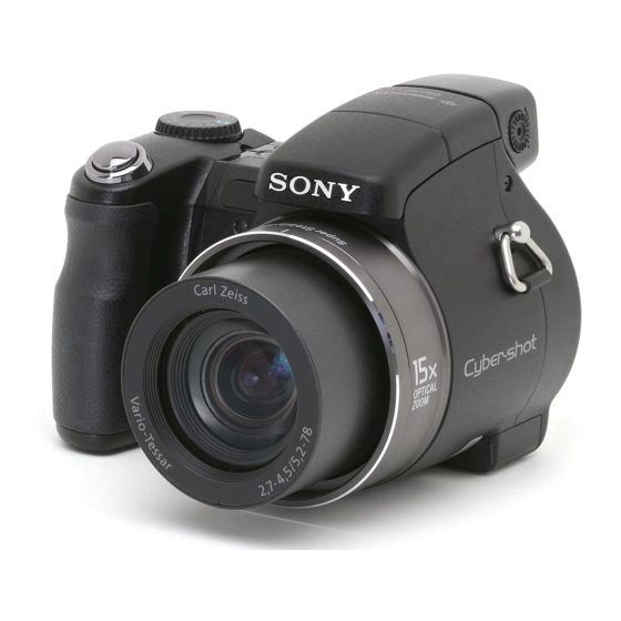
Photo: DSC-H7 Black Model
PRINTED WIRING BOARDS
REPAIR PARTS LIST
Les composants identifiés par une
marque 0 sont critiques pour la
sécurité.
Ne les remplacer que par une pièce
portant le numéro spécifié.
Sony EMCS Co.
DSC-H7 / H9
DIGITAL STILL CAMERA
3
LEVEL
US Model
Canadian Model
AEP Model
UK Model
E Model
Australian Model
Hong Kong Model
Chinese Model
Korea Model
Argentine Model
Brazilian Model
Tourist Model
Japanese Model
2007E0200-1
© 2007.5
Published by Kohda TEC
Advertisement

Related Manuals for Sony DSC-H7


Summary of Contents for Sony DSC-H7
- Page 1 Manual. Chinese Model Korea Model Internal memory Internal memory Argentine Model ON BOARD ON BOARD Brazilian Model Photo: DSC-H7 Black Model Tourist Model Japanese Model Link Link SERVICE NOTE PRINTED WIRING BOARDS SCHEMATIC DIAGRAMS REPAIR PARTS LIST The components identified by Les composants identifiés par une...
- Page 2 CRITIQUES POUR LA SÉCURITÉ DE FONCTIONNEMENT. NE COMPONENTS WITH SONY PARTS WHOSE PART NUMBERS REMPLACER CES COMPOSANTS QUE PAR DES PIÈSES SONY APPEAR AS SHOWN IN THIS MANUAL OR IN SUPPLEMENTS DONT LES NUMÉROS SONT DONNÉS DANS CE MANUEL OU PUBLISHED BY SONY.
-
Page 3: Table Of Contents
1-4. Method for Copying or Erasing the Data in Internal Memory ··········································································· 1-2 PRINTED WIRING BOARDS AND SCHEMATIC DIAGRAMS 4-2. Schematic Diagrams ························································ 4-2 4-3. Printed Wiring Boards ··················································· 4-22 4-4. Mounted Parts Location ················································ 4-30 REPAIR PARTS LIST 5-2. Electrical Parts List ······················································· 5-11 DSC-H7/H9_L3 — 3 —... -
Page 4: Service Note
1 Select [Format] with v/V/b/B on the control button, then press z. The message “All data in internal memory will be erased” appears. 2 Select [OK] with v, then press z. The format is completed. To cancel the formatting Select [Cancel] in step 2, then press z. DSC-H7/H9_L3... -
Page 5: Schematic Diagrams
SY-177 BOARD (4/7) DD-272 BOARD (2/3) ( CAMERA DSP/SYSTEM CONTROL ( 2 )) ( DC-DC CONVERTER, SYSTEM CONTROL ) DD-272 BOARD (3/3) SY-177 BOARD (5/7) ( CAMERA DSP/SYSTEM CONTROL ( 3 )) ( FLASH/CHARGE CONTROL ) COMMON NOTE FOR SCHEMATIC DIAGRAMS DSC-H7/H9_L3... - Page 6 In addition, ensure that the receiver is not covered with Les composants identifiés par une marque 0 sont dusts nor exposed to strong light. critiques pour la sécurité. Ne les remplacer que par une pièce portant le numéro spécifie. DSC-H7/H9_L3...
- Page 7 PITCH_HALLBAIS+ 0.1u 0.1u 0.1u PITCH_HALLBAIS+ PITCH_HALL+ PITCH_HALL+ R414 PITCH_HALLBAIS- (7/7) PITCH_HALLBAIS- 100k PITCH+ PITCH+ PITCH- PITCH- Q402 YAW+ MTM231230LSO YAW+ R415 YAW- YAW- TZ_HALL_TEMP TZ_HALL_TEMP R:-7.4/P:3.1 Q402,403 LENS_TEMP LENS_TEMP SWITCH (4/7) Q403 R:-7.4 CAM_–7.5V P:3.1 EMD12T2R R:-7.5/P:0 DSC-H7/H9_L3 SY-177 (1...
- Page 8 +13V REG. R:13.7/P:0 REG_GND R328 IC303 C324 NJM2831F13(TE1) CAM-7.5V CAM_-7.5V FB301 CAM_–7.5V REG_GND D301 CAM_12V R321 1SS387CT(TL3SONY) R301 R:-7.5 C304 C306 C326 R303 0.1u Q303 R302 150k C301 R304 SSM3J15FV(TL3SONYZ) 0.0022u 100k SWITCH R325 100k Q301 DTC144EMT2L SWITCH DSC-H7/H9_L3 SY-177 (2...
- Page 9 (4/7) C201 IC_211_1_UI CN704 (2/5) 0.1u IC_211_1_UI IC_211_1_UO CAMERA DSP/ KEY_AD2 IC_211_1_UO GNDS Note: It is connected to CN201 of PL-046 (DSC-H7) (6/7) USB_DP MODE_DIAL1 USB_DP SYSTEM CONTROL USB_DM or PL-047 (DSC-H9) (Page 4-16 of LEVEL2) MODE_DIAL2 USB_DM (4/7) AVDD1 C3 D3 E3 A4 B4 C4 through the flexible flat cable (PL-002).
- Page 10 R259 VDDO GEAR_ON 2200 IC_211_PROUT (5/7)(7/7) C203 SYS_OUT VDDO BL_L Q244 BL_L 0.1u VOUT2 AC12 C207 2SA2029T2LQ/R R262 BL_H 4.7u BL_H BUFFER (5/7) IC202 GEN_SYS_CLK (3/7) R210 X201 CLOCK GENERATOR 36MHz L242 10uH C250 C206 0.1u REG_GND DSC-H7/H9_L3 SY-177 (4...
- Page 11 D_1.2V D_1.8V (2/7)(4/7)(7/7) D_1.8V D_1.8V DDR_1.8V DDR_1.8V REG_GND (2/7) CAM_12V CAM_12V (1/7)(2/7) CAM_-7.5V CAM_-7.5V REG_GND REG_GND (1/7)(3/7)(4/7)(6/7)(7/7) A_3.0V A_3.0V A_3.0V ACV_UNREG2 ACV_UNREG2 (6/7) ACV_UNREG2 ACV_UNREG2 ACV_UNREG2 MS_VCC MS_VCC (3/7) MS_VCC (4/7) PANEL_6.4V PANEL_6.4V LND001 (6/7) STATIC_GND STATIC_GND DSC-H7/H9_L3 SY-177 (5...
- Page 12 IC_211_1_UO R608 IC_211_1_UO(UART_Tx) IC_211_1_UO (3/7) C608 C615 IC_211_1_UO IC_211_1_UI IC_211_1_UI(UART_Rx) IC_211_1_UI C613 IC_211_1_UI BATT/XEXT BATT/XEXT R606 D602 ACV_UNREG2 D_3.0V MA2S111-(K8).SO C711 BATT/XEXT BATT/XEXT ACV_UNREG2 (5/7) C712 ACV_UNREG2 ACV_UNREG2 D703 MAZS068008SO D701 D702 MAZW068H0LS0 MAZW068H0LS0 (5/7) STATIC_GND REG_GND DSC-H7/H9_L3 SY-177 (6...
- Page 13 YAW+ YAW+ YAW- C507 YAW- 0.1u PITCH_HALL+ R506 PITCH_HALL+ 2200 PITCH_HALL- PITCH_HALL- PITCH_HALLBAIS+ PITCH_HALLBAIS+ (1/7) PITCH_HALLBAIS- PITCH_HALLBAIS- YAW_HALL+ YAW_HALL+ YAW_HALL- YAW_HALL- YAW_HALLBAIS+ YAW_HALLBAIS+ C516 YAW_HALLBAIS- 0.01u YAW_HALLBAIS- C514 R515 0.0022u C510 0.0022u C509 C513 0.01u 0.01u DSC-H7/H9_L3 SY-177 (7 4-10...
- Page 14 D003 R074 XSTRB_FULL Q014 MA2SD32008S0 4700 XSTRB_FULL SSM6E01TU STRB_ON DDCPV_EN SWITCH STRB_ON R:13.7/P:0 1.2V_INT STRB_CHG_CONT R083 R016 @104 STRB_CHG_CONT DDC2P9_EN DSC-H7 DSC-H7 DDC2P9_EN USB_VBUS C013 D007 R042 USB_VBUS DSC-H9 DSC-H9 L004 DDC1P8_EN (2/3) MA2SD32008S0 680k DDC1P8_EN XMS_IN 4.7uH XMS_IN R030...
- Page 15 XRESET_REQ 1.2V_INT DDCPV_EN XCS_FR CL124 Q101 EMH3T2R INVERTER B2 B1 C2 C1 D3 D1 D2 E1 E2 H3 J3 J2 G4 A9 B9 C8 CL123 CL122 R105 REG_GND C103 C104 0.1u 0.01u CL101 CL118 CL119 CL120 DSC-H7/H9_L3 DD-272 (2 4-19...
- Page 16 LEVEL2 R204 R209 IC201 R213 PGND Q203 GPS_13 DTC144EMT2L PGND LND202 TI_5.0V FLASH/CHARGE SWITCH REG_GND CONTROL R205 F_ON XFULL XDD_SYS_RST IC201 D203 MA2SD32008S0 TPS65552RGTR C203 C206 STRB_ON R206 @102 (1/3) CL201 STRB_CHG_CONT XSTRB_FULL STRB_CHG C204 REG_GND DSC-H7/H9_L3 DD-272 (3 4-20...
-
Page 17: Printed Wiring Boards
All manuals and user guides at all-guides.com 4-3. PRINTED WIRING BOARDS Link Link SY-177 BOARD DD-272 BOARD COMMON NOTE FOR PRINTED WIRING BOARDS MOUNTED PARTS LOCATION DSC-H7/H9_L3... - Page 18 All manuals and user guides at all-guides.com 4-3. PRINTED WIRING BOARDS 4-3. PRINTED WIRING BOARDS 4-3. PRINTED WIRING BOARDS THIS NOTE IS COMMON FOR PRINTED WIRING BOARDS • Chip parts. • : Uses unleaded solder. • : Circuit board Transistor Diode : Flexible board Pattern from the side which enables seeing.
- Page 19 IC306 IC305 FB306 R752 C711 C712 R732 D701 CAM_12V FB303 R320 A_3.0V C703 D_1.8V C318 CAM_12V D703 IC701 C325 R318 CN707 C302 L301 C305 R312 R325 R311 R337 C707 D_3.0V L302 R321 C705 1-871-925- Q303 CN301 1-871-925- DSC-H7/H9_L3 SY-1 4-23...
- Page 20 Note: DD-272基板のリチウム電池 (BT001) を交換 する場合はバッテリホルダ (BH101) も同時に 新品に交換して下さい。 ( 一度使用したバッテ リホルダは再使用できません。 ) 部品取付けの際は、 先にバッテリホルダを取 付けてからリチウム電池を装着して下さい。 CAUTION Danger of explosion if battery is incorrectly replaced. Replace only with the same or equivalent type. 注意 電池の交換は、 正しく行わないと破裂する恐れがあ ります。 電池を交換する場合には必ず同じ型名の電 池又は同等品と交換してください。 DSC-H7/H9_L3 DD-2 4-24...
-
Page 21: Mounted Parts Location
All manuals and user guides at all-guides.com 4-3. PRINTED WIRING BOARDS 4-3. PRINTED WIRING BOARDS 4-4. MOUNTED PARTS LOCATION no mark : side A * mark : side B DD-272 BOARD SY-177 BOARD BH001 A-1 F001 R114 * C201 C505 FB212 BH101 A-2 F002... - Page 22 * R604 * R605 * R606 * R607 * R608 * R609 * R707 * R709 * R710 * R711 * R712 * R713 R718 R719 * R720 R732 * R750 R752 R753 R757 * R758 R802 R804 DSC-H7/H9_L3 SY-177 4-31E...
-
Page 23: Repair Parts List
All manuals and user guides at all-guides.com 5. REPAIR PARTS LIST NOTE: • -XX, -X mean standardized parts, so they may have some differences from When indicating parts by reference number, the original one. please include the board name. • Items marked “*” are not stocked since they are seldom required for routine The components identified by mark 0 or service. -
Page 24: Electrical Parts List
10% 6.3V Note: DD-272基板のリチウム電池 (BT001) を交換する場合はバッ C101 1-125-777-11 CERAMIC CHIP 0.1UF 10% 10V テリホルダ (BH101) も同時に新品に交換して下さい。 ( 一度使 用したバッテリホルダは再使用できません。 ) C102 1-125-777-11 CERAMIC CHIP 0.1UF 10% 10V 部品取付けの際は、 先にバッテリホルダを取付けてからリチ ウム電池を装着して下さい。 • Refer to page 5-1 for mark 0. DSC-H7/H9_L3 5-11... - Page 25 < VIBRATOR > R011 1-208-927-11 METAL CHIP 0.5% 1/16W R012 1-208-939-11 METAL CHIP 150K 1/16W R013 1-208-715-11 METAL CHIP 1/16W X101 1-781-525-21 VIBRATOR, CRYSTAL (32.768kHz) R014 1-208-935-11 METAL CHIP 100K 0.5% 1/16W • Refer to page 5-1 for mark 0. DSC-H7/H9_L3 5-12...
- Page 26 1-125-777-11 CERAMIC CHIP 0.1UF 10% 10V C315 1-112-716-11 CERAMIC CHIP 0.1UF 10% 6.3V C555 1-165-908-11 CERAMIC CHIP 10% 10V C316 1-112-716-11 CERAMIC CHIP 0.1UF 10% 6.3V C556 1-165-908-11 CERAMIC CHIP 10% 10V • Refer to page 5-1 for mark 0. DSC-H7/H9_L3 5-16...
- Page 27 6-500-776-01 DIODE MAZW068H0LS0 Q302 8-729-054-47 TRANSISTOR UP04213008S0 D702 6-500-776-01 DIODE MAZW068H0LS0 Q303 6-550-791-01 TRANSISTOR SSM3J15FV (TL3SONYZ) Q401 8-729-054-51 TRANSISTOR UP04116008S0 Q402 6-551-304-01 TRANSISTOR MTM231230LSO D703 8-719-056-54 DIODE MAZS068008SO Q403 6-550-025-01 TRANSISTOR EMD12T2R < TERMINAL > Q702 8-729-053-52 TRANSISTOR HN1C01FE-Y/GR (TPLR3) DSC-H7/H9_L3 5-17...
- Page 28 1-218-990-81 SHORT CHIP R318 1-218-990-81 SHORT CHIP R713 1-218-952-11 RES-CHIP 1/16W R718 1-211-982-11 METAL CHIP 0.5% 1/10W R719 1-211-982-11 METAL CHIP 0.5% 1/10W R319 1-218-990-81 SHORT CHIP R320 1-218-990-81 SHORT CHIP R720 1-218-953-11 RES-CHIP 1/16W R321 1-218-941-81 RES-CHIP 1/16W DSC-H7/H9_L3 5-18...
- Page 29 1-234-375-21 RES, NETWORK 1K (1005X4) < SENSOR > SE501 1-479-022-51 SENSOR, ANGULAR VELOCITY (30.8KHZ) (PITCH) SE502 1-479-022-61 SENSOR, ANGULAR VELOCITY (32.2KHZ) (YAW) < TERMINAL > TB001 1-780-112-11 TERMINAL, CONTACT < VIBRATOR > * X201 1-813-860-21 OSCILLATOR, CRYSTAL (36MHz) DSC-H7/H9_L3 5-19...
- Page 30 All manuals and user guides at all-guides.com Reverse 985220312.pdf Revision History S.M. Rev. Ver. Date History Contents issued 2007.04 Official Release — — • Correction of SCHEMATIC DIAGRAMS 2007.05 Revised-1 • Correction of PRINTED WIRING BOARDS DSC-H7/H9_L3...
Need help?
Do you have a question about the DSC-H7 and is the answer not in the manual?
Questions and answers