
Subscribe to Our Youtube Channel
Related Manuals for Sylvania 6509DD


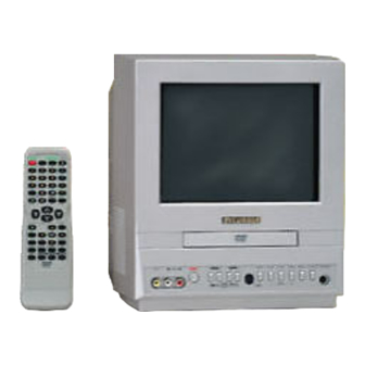
Summary of Contents for Sylvania 6509DD
- Page 1 SERVICE MANUAL Sec. 1: Main Section Sec. 2: Exploded views and Parts List Section I Specifications I Adjustment Procedures I Exploded views I Parts List I Schematic Diagrams I CBA’s 9" COLOR TV/DVD 6509DD/SSC509D...
- Page 2 IMPORTANT SAFETY NOTICE Proper service and repair is important to the safe, reliable operation of all Funai Equipment. The service procedures recommended by Funai and described in this service manual are effective methods of performing service operations. Some of these service special tools should be used when and as recommended.
-
Page 3: Table Of Contents
MAIN SECTION 9" COLOR TV/DVD 6509DD/SSC509D Sec. 1: Main Section I Specifications I Adjustment Procedures I Schematic Diagrams I CBA’s TABLE OF CONTENTS Specifications................1-1-1 Laser Beam Safety Precautions. -
Page 4: Specifications
SPECIFICATIONS < TV Section > *ˆ M ode---------SP mode unless otherwise specified *Test input terminal <Except Tuner>-------------Video input (1Vp-p) Audio input (-10dB) <Tuner>-----------------------Ant. input (80dBµV) Video: 87.5% Audio: 25kHz dev (1kHz Sin) <DEFLECTION> Description Condition Unit Nominal Limit 1. Over Scan —... - Page 5 <DVD Section> ITEM CONDITIONS UNIT NOMINAL LIMIT 1. Video Output 75 ohm load ± 0.1 2. Coaxial Digital Out 75 ohm load mVpp ± 100 3. Audio (PCM) 3-1. Output Level 1kHz 0dB Vrms 3-2. S/N 3-3. Freq. Response fs=48kHz 20~22kHz ±...
-
Page 6: Laser Beam Safety Precautions
LASER BEAM SAFETY PRECAUTIONS This DVD player uses a pickup that emits a laser beam. Do not look directly at the laser beam coming from the pickup or allow it to strike against your skin. The laser beam is emitted from the location shown in the figure. When checking the laser diode, be sure to keep your eyes at least 30cm away from the pickup lens when the diode is turned on. -
Page 7: Important Safety Precautions
IMPORTANT SAFETY PRECAUTIONS Prior to shipment from the factory, our products are strictly inspected for recognized product safety and electrical codes of the countries in which they are to be sold. However, in order to maintain such compliance, it is equally important to implement the following precautions when a set is being serviced. - Page 8 ing is performed that involves B+, horizontal de- earth ground. If a voltage reading in excess of 1.0V flection or high voltage. Correct operation of the is obtained, remove and reinsert the AC power X-radiation protection circuits also must be recon- plug in the opposite polarity and again measure firmed each time they are serviced.
- Page 9 Precautions during Servicing H. When a power cord has been replaced, check that 5~6 kg of force in any direction will not loosen it. A. Parts identified by the ( # ) symbol are critical for I. Also check areas surrounding repaired locations. safety.
- Page 10 Safety Check after Servicing Examine the area surrounding the repaired location for damage or deterioration. Observe that screws, Chassis or Secondary Conductor parts and wires have been returned to original posi- tions. Afterwards, perform the following tests and con- Primary Circuit Terminals firm the specified values in order to verify compliance with safety standards.
-
Page 11: Standard Notes For Servicing
STANDARD NOTES FOR SERVICING Circuit Board Indications How to Remove / Install Flat Pack IC 1. The output pin of the 3 pin Regulator ICs is indi- Caution: cated as shown: 3. Do not apply the hot air to the chip parts around the Flat Pack-IC for over 6 seconds as damage may occur to the chip parts. - Page 12 b. The "I" mark on the Flat Pack - IC indicates pin 1 (See Fig. S-1-6). Make sure this mark matches the 1 on the CBA when positioning for installation. Then pre - solder the four corners of the Flat Pack- IC (See Fig.
- Page 13 Instructions for Handling Presolder Semiconductors Electrostatic breakdown of the semiconductors may occur due to a potential difference caused by electro- static charge during unpacking or repair work. Ground for Human Body Be sure to wear a grounding band (1MΩ) that is prop- erly grounded to remove any static electricity that may be charged on the body.
-
Page 14: Operating Controls And Functions
OPERATING CONTROLS AND FUNCTIONS TV/DVD FRONT PANEL TV/DVD REAR VIEW DC 13.2V ANT. AUDIO OUT VIDEO AUDIO POWER VOLUME CHANNEL STOP SKIP PLAY SKIP PAUSE OPEN/CLOSE HEADPHONE COAXIAL SEARCH 8 9 101112 13 14 REMOTE CONTROL OPEN/ POWER PICTURE SELECT CLOSE 6. - Page 15 30. RETURN Button 16. Number Button Returns to the previous operation. TV Mode: Press two digits to directly access the desired 31. ENTER Button channel. Press to accept a setting. Remember to press a "0" before a single digit 32. Arrow Buttons channel.
-
Page 16: Cabinet Disassembly Instructions
CABINET DISASSEMBLY INSTRUCTIONS 1. Disassembly Flowchart (1): Order of steps in Procedure. When reassembling, follow the steps in reverse order.These numbers This flowchart indicates the disassembly steps for the are also used as the identification (location) No. of cabinet parts, and the CBA in order to gain access to parts in Figures. - Page 17 [1] REAR CABINET Fig. 1 Anode Cap CRT CBA [4] CRT Fig. 2 1-6-2 TD001DC...
- Page 18 [5] Shield Box [3] Tray Chassis [6] DVD Mechanism Shield Case Top S-10 S-10 [8] Main CBA [9] H.V./DC Power Supply CBA Shield Case Bottom [2] H.V. CBA (wih Holder) Fig. 3 1-6-3 TD001DC...
- Page 19 CN201 [7] DVD Main CBA Unit CN301 DVD Mechanism Short the three short lands by soldering Slide Pickup Unit View for A View for B Fig. 4 1-6-4 TD001DC...
- Page 20 ANODE CRT CBA DVD MAIN CBA UNIT SCREEN CN601 WH501 FOCUS CN501 CN401 SPEAKER CN1802 CN1603 CN1731 CN1604 MAIN CBA CN1601 CORD CN1302 CN1801 SPEAKER WH552 WH551 WH554A CN571 H.V./DC POWER SUPPLY Fig. 5 1-6-5 TD001DC...
-
Page 21: Electrical Adjustment Instructions
ELECTRICAL ADJUSTMENT INSTRUCTIONS General Note: How to Set up the Service mode: "CBA" is abbreviation for "Circuit Board Service Mode: Assembly." 1. Use the service remote control unit. NOTE: 2. Turn the power on. Electrical adjustments are required after replacing cir- 3. - Page 22 1b. DC 117V (+B) Adjustment 3-1. Setting for Data Values (DC Power) General 1. Enter the Service mode. (See page 1-7-1) Purpose: To obtain correct operation. 2. To select the Data Value, press "VOL p" button on Symptom of Misadjustment: The picture is dark and the service remote control unit.
- Page 23 4. V. Size Adjustment 6. H. Position Adjustment Purpose: To obtain correct vertical height of screen Purpose: To obtain correct horizontal position of image. screen image. Symptom of Misadjustment: If H. Position is incor- Symptom of Misadjustment: If V. Size is incorrect, rect, horizontal position of image on the screen may vertical height of image on the screen may not be not be properly displayed.
- Page 24 7. White Balance Adjustment 8. Sub-Brightness Adjustment Purpose: To mix red, green and blue beams correctly Purpose: To get proper brightness. for pure white. Symptom of Misadjustment: If Sub-Brightness is incorrect, proper brightness cannot be obtained by Symptom of Misadjustment: White becomes bluish adjusting the Brightness Control.
- Page 25 9. Focus Adjustment 10. C-Trap Adjustment Purpose: Set the optimum Focus. Purpose: To get minimum leakage of the color signal carrier. Symptom of Misadjustment: If Focus Adjustment is incorrect, blurred images are shown on the display. Symptom of Misadjustment: If C-Trap Adjustment is incorrect, stripes will appear on the screen.
- Page 26 11. H f o Adjustment 12. Y DL Time/Y SW LPF Adjustment Purpose: To get correct horizontal frequency. Symptom of Misadjustment: If H f 0 adjustment is in Purpose: To get minimum leakage of the color signal correct, skew distortion will appear on the screen. carrier.
- Page 27 13. Cut-off Adjustment The following 2 adjustments normally are not attempted in the field. They should be done Purpose: To adjust the beam current of R, G, B, and only when replacing the CRT then adjust as a screen voltage. preparation.
- Page 28 15. Convergence Adjustment Purpose: To obtain proper convergence of red, green and blue beams. Symptom of Misadjustment: If Convergence Adjust- ment is incorrect, the edge of white letters may have color edges. Test point Adj. Point Mode Input C.P. Magnet (RB), Dot Pattern C.P.
-
Page 29: Firmware Renewal Mode
FIRMWARE RENEWAL MODE 1. Turn the power on and remove the disc on the tray. 5. After programming is finished, the tray opens auto- 2. To put the DVD player into version up mode, press matically. Fig. c appears on the screen. [9], [8], [7], [6], and [SEARCH MODE] buttons on the remote control unit in that order. - Page 30 BLOCK DIAGRAMS < TV SECTION > Video/System Control Block Diagram DVD VIDEO SIGNAL VIDEO (TUNER/LINE) SIGNAL MAIN CBA IC1201 X1301 TV MICON/VIDEO 3.58MHz /CHROMA TU1001 /DEFLECTION (TUNER UNIT) C1603 Q1621 FROM/TO DVD SYSTEM VIDEO SDATA Q1622 CONTROL BLOCK SDATA SCLK (DVD SECTION) Q1623 REMOTE...
- Page 31 Audio Block Diagram AUDIO (TV/LINE) SIGNAL DVD AUDIO SIGNAL MAIN CBA JK1730 Q1731 DVD DIGITAL AUDIO OUT TP1402 (COAXIAL) AUDIO-R-OUT IC1731 (AMP) WF20 AUDIO(R) CN1731 TP1401 SPDIF 1 AUDIO-L-OUT TO DVD AUDIO DVD-AUDIO(R) 4 BLOCK DVD-AUDIO(L) 6 (DVD SECTION) AUDIO(L) DVD-A-MUTE 7 WF19 Q1734...
- Page 32 CRT/H.V. Block Diagram DVD VIDEO SIGNAL VIDEO SIGNAL(TUNER/LINE) IC551 (VERTICAL DEFLECTION CONTROL) L1551 D.Y. WF12 THERMAL WF11 PROTECTION DRIVE Q572 H.DRIVE PULSE DRIVE Q571 CN571 T572 H.OUTPUT J109 +B ADJ FROM POWER SUPPLY BLOCK FOCUS VR DEF+B T571 F.B.T. ANODE FOCUS SCREEN ANODE...
- Page 33 Power Supply Block Diagram CAUTION ! Fixed voltage ( or Auto voltage selectable ) power supply circuit is used in this unit. NOTE : If Main Fuse (F1601) is blown, check to see that all components in the power supply CAUTION: FOR CONTINUED PROTECTION AGAINST RISK OF FIRE, The voltage for parts in hot circuit is measured using...
- Page 34 DC Power Supply Block Diagram Fixed voltage power supply circuit is used in this unit. CAUTION: FOR CONTINUED PROTECTION AGAINST RISK OF FIRE, If Main Fuse (F951) is blown, check to see that all components in the power supply REPLACE ONLY WITH SAME TYPE 8 A, 125V FUSE. circuit are not defective before you connect the DC plug to the DC power supply.
- Page 35 BLOCK DIAGRAMS < DVD Section > DVD System Control/Servo Block Diagram FOCUS SERVO SIGNAL TRACKING SERVO SIGNAL SLED SERVO SIGNAL SPINDLE SERVO SIGNAL IC101 (MICRO CONTROLLER) EXT CLOCK CLK33M BE CLOCK IC451 (CLOCK GENERATOR) X451 MULTI X'TAL 36.864MHz PLL2 FSEL PCM-SCLK A-MUTE A-MUTE...
-
Page 36: Block Diagrams
Digital Signal Process Block Diagram DATA(AUDIO) SIGNAL DATA(VIDEO/AUDIO) SIGNAL DVD VIDEO SIGNAL FOCUS SERVO SIGNAL TRACKING SERVO SIGNAL IC102 (SDRAM) IC101 (MICRO CONTROLLER) SDRAM ADDRESS(0-10) SDRAM ADDRESS(0-10) DATA SDRAM EXTERNAL MEMORY DECODER INST. DECODER STREAM SDRAM DATA(0-31) SDRAM DATA(0-31) DATA PIXEL OPERATION INST. - Page 37 DVD Audio Block Diagram DVD AUDIO SIGNAL DATA(AUDIO) SIGNAL IC601 (AUDIO DAC) SPDIF FROM L-CH 4X/8X DIGITAL LPF+AMP PCM-BCK OVERSAMPLING ENPHANCED SIGNAL SERIAL PCM-DATA0 DIGITAL FILTER MULTI-LEVEL PROCESS PORT PCM-LRCLK /FUNCTION DELTA-SIGMA BLOCK R-CH MODULATOR LPF+AMP CONTROLLER DIAGRAM CN601 12 SPDIF TO AUDIO BLOCK 7 DVD-AUDIO(L) (TV SECTION)
-
Page 38: Schematic Diagrams / Cba's And Test Points
SCHEMATIC DIAGRAMS / CBA’S AND TEST POINTS Standard Notes Note: 1. Do not use the part number shown on these draw- Warning ings for ordering. The correct part number is shown in the parts list, and may be slightly different or Many electrical and mechanical parts in this chassis amended since these drawings were prepared. - Page 39 LIST OF CAUTION, NOTES, AND SYMBOLS USED IN THE SCHEMATIC DIAGRAMS ON THE FOLLOWING PAGES: 1. CAUTION: FOR CONTINUED PROTECTION AGAINST RISK OF FIRE, REPLACE ONLY WITH SAME TYPE_A,_V FUSE. ATTENTION: UTILISER UN FUSIBLE DE RECHANGE DE MÊME TYPE DE_A,_V. 2.
- Page 40 Main 1/5 Schematic Diagram < TV Section > VIDEO (TV/LINE) + DVD VIDEO SIGNAL VIDEO (TV/LINE) SIGNAL DVD VIDEO SIGNAL MAIN 1/5 Ref No. Position IC1201 TRANSISTORS Q1261 Q1301 Q1350 CONNECTOR CN1302 TEST POINTS TP1301 TP1302 TP1303 1-10-3 1-10-4 TD001SCM1...
- Page 41 Main 2/5 Schematic Diagram < TV Section > VIDEO (TV/LINE) + DVD VIDEO SIGNAL AUDIO (TV/LINE) SIGNAL VIDEO (TV/LINE) SIGNAL DVD AUDIO SIGNAL DVD VIDEO SIGNAL MAIN 2/5 Ref No. Position IC1202 IC1451 IC1452 IC1731 TRANSISTORS Q1453 Q1454 CONNECTOR CN1731 TEST POINTS TP1401 TP1402...
- Page 42 Main 3/5 Schematic Diagram < TV Section > DVD VIDEO SIGNAL AUDIO (TV/LINE) SIGNAL DVD AUDIO SIGNAL MAIN 3/5 Ref No. Position IC1801 TRANSISTORS Q1282 Q1731 Q1732 Q1733 Q1734 Q1736 Q1737 Q1738 CONNECTORS CN1801 CN1802 TEST POINTS TP1731 TP1733 TP1734 1-10-7 1-10-8 TD001SCM3...
- Page 43 Main 4/5 Schematic Diagram < TV Section > CAUTION ! Fixed voltage ( or Auto voltage selectable ) power supply circuit is used in this unit. CAUTION: FOR CONTINUED PROTECTION AGAINST RISK NOTE : If Main Fuse (F601) is blown, check to see that all components in the power supply OF FIRE, REPLACE ONLY WITH SAME TYPE 4A, 125V FUSE.
- Page 44 Main 5/5 Schematic Diagram < TV Section > MAIN 5/5 Ref No. Position IC1602 IC1603 AA-3 IC1604 TRANSISTORS Q1619 AA-3 Q1621 BB-2 Q1622 BB-2 Q1623 BB-1 Q1625 BB-3 CONNECTORS CN1602 CN1603 CC-3 TD001SCM5 1-10-11 1-10-12...
- Page 45 H.V. / DC Power Supply 1/2 & CRT Schematic Diagram < TV Section > H.V./DC POWER SUPPLY 1/2 Ref No. Position Ref No. Position TRANSISTORS IC551 Q501 TRANSISTORS Q502 Q571 Q503 Q572 CONNECTORS Q591 CN501 CONNECTORS WH501 CN571 WH551 WH552 TEST POINTS J109 J551...
- Page 46 H.V. / DC Power Supply 2/2 Schematic Diagram < TV Section > H.V./DC POWER SUPPLY 2/2 CAUTION ! Ref No. Position Fixed voltage power supply circuit is used in this unit. CAUTION: FOR CONTINUED PROTECTION AGAINST RISK If Main Fuse (F951) is blown, check to see that all components in the power supply OF FIRE, REPLACE ONLY WITH SAME TYPE 8A, 125V FUSE.
- Page 47 DVD Main 1/3 Schematic Diagram < DVD Section > DATA(VIDEO+AUDIO) FOCUS SERVO SIGNAL SPINDLE SERVO SIGNAL TRACKING SERVO SIGNAL SLED SERVO SIGNAL DVD MAIN 1/3 Ref No. Position IC201 IC202 IC301 IC461 TRANSISTORS Q251 Q252 Q253 Q254 CONNECTORS CN201 CN301 CN401 1-10-17 1-10-18...
- Page 48 DVD Main 2/3 Schematic Diagram < DVD Section > DATA(VIDEO+AUDIO) SPINDLE SERVO SIGNAL DATA (AUDIO) FOCUS SERVO SIGNAL TRACKING SERVO SIGNAL DVD VIDEO SIGNAL SLED SERVO SIGNAL DVD MAIN 2/3 Ref No. Position IC101 1-10-19 1-10-20 TD001SCD2...
- Page 49 IC101 VOLTAGE CHART PIN.NO PLAY STOP PIN.NO PLAY STOP PIN.NO PLAY STOP PIN.NO PLAY STOP PIN.NO PLAY STOP PIN.NO PLAY STOP PIN.NO PLAY STOP PIN.NO PLAY STOP ----- ----- ----- ----- ----- ----- ----- ----- ----- ----- ----- ----- ----- ----- ----- -----...
- Page 50 DVD Main 3/3 Schematic Diagram < DVD Section > DVD VIDEO SIGNAL DVD AUDIO SIGNAL DATA (AUDIO) DVD MAIN 3/3 Ref No. Position IC102 IC103 IC104 IC105 IC451 IC601 CONNECTOR CN601 1-10-23 1-10-24 TD001SCD3...
- Page 51 Main CBA Top View < TV Section > CAUTION ! BECAUSE A HOT CHASSIS GROUND IS PRESENT IN THE POWER CAUTION: FOR CONTINUED PROTECTION AGAINST RISK Fixed voltage ( or Auto voltage selectable ) power supply circuit is used in this unit. OF FIRE, REPLACE ONLY WITH SAME TYPE 4A, 125V FUSE.
- Page 52 Main CBA Bottom View < TV Section > CAUTION: FOR CONTINUED PROTECTION AGAINST RISK BECAUSE A HOT CHASSIS GROUND IS PRESENT IN THE POWER CAUTION ! OF FIRE, REPLACE ONLY WITH SAME TYPE 4A, 125V FUSE. Fixed voltage ( or Auto voltage selectable ) power supply circuit is used in this unit. SUPPLY CIRCUIT, AN ISOLATION TRANSFORMER MUST BE USED.
- Page 53 H.V. /DC POWER SUPPLY CBA Top View < TV Section > CAUTION: FOR CONTINUED PROTECTION AGAINST RISK CAUTION ! OF FIRE, REPLACE ONLY WITH SAME TYPE 4A, 125V FUSE. Fixed voltage ( or Auto voltage selectable ) power supply circuit is used in this unit. ATTENTION: UTILISER UN FUSIBLE DE RECHANGE DE If Main Fuse (F951) is blown, check to see that all components in the power supply 8A 125V...
- Page 54 H.V. /DC POWER SUPPLY CBA Bottom View < TV Section > CAUTION: FOR CONTINUED PROTECTION AGAINST RISK CAUTION ! OF FIRE, REPLACE ONLY WITH SAME TYPE 4A, 125V FUSE. Fixed voltage ( or Auto voltage selectable ) power supply circuit is used in this unit. ATTENTION: UTILISER UN FUSIBLE DE RECHANGE DE If Main Fuse (F951) is blown, check to see that all components in the power supply 8A 125V...
- Page 55 CRT CBA Top View < TV Section > CRT CBA Bottom View < TV Section > CRT CBA Ref No. Position TRANSISTORS Q501 Q502 Q503 CONNECTORS CN501 WH501 WF15 WF14 Q501 Q501 Q502 Q502 Base Base Collector Collector WF13 Q503 Q503 Collector Base...
- Page 56 Junction-A CBA Junction-A CBA Bottom View < TV Section > Top View < TV Section > BT700F01022-B Junction-B CBA Junction-B CBA Bottom View < TV Section > Top View < TV Section > BT700F01022-C 1-10-35 1-10-36...
-
Page 57: Waveforms
WAVEFORMS Input: NTSC Color Bar Signal ( with 1kHz Audio Signal ) --- WF1~WF16 DVD Video( Power on ( Stop ) MODE ) --- WF17, WF18 CD( 1KHz Play ) --- WF19, WF20 WF1 ~ WF20 = Waveforms to be observed at INITIAL POSITION: Unplug unit from AC outlet for at least 5 minutes. -
Page 58: Wiring Diagrams
WIRING DIAGRAM JUNCTION-A CBA BTD700F01022-B CN1604 CN901A WH555A WH554A DVD-MAIN-POWER 1 1 DVD-MAIN-POWER CN1801 2 GND SP1801 CL1801 1 SP-R AL+9V 3 AL+9V SPEAKER 2 SP-GND R CH 4 GND 5 GND P-ON+12V 6 P-ON+12V CN1802 SP1802 CL1802 7 GND 1 SP-L SPEAKER DC+13.2V... -
Page 59: System Control Timing Charts
SYSTEM CONTROL TIMING CHARTS Tray Close ~ Play / Play ~ Tray Open Disc Tray Tray Disc Stop Open Close Rotation Play 3.3V Tray OUT (TL220) 3.3V Tray IN (TL221) 1.65V Sled Drive (TP303) 1.65V Disc Drive (TP301) 1.65V Focus Drive (TP304) 1.65V Tracking Drive... -
Page 60: Ic Pin Functions
IC PIN FUNCTIONS IC1201 (TV Micro Computer) Signal Name Function Signal Name Function 35 N.U. Not Used 36 N.U. Not Used 37 V RAMP F/B V Ramp Feed Back Input for Oscillator 38 V RAMP OUT Vertical Output XOUT Output for Oscillator 39 V RAMP CAP V Ramp OSC Capacitor TEST 1... - Page 61 Signal Name Function 68 AGC-IN AGC Voltage Input 69 AFT AFT Voltage Input 70 REMOTE Input for Remote Control 71 N.U. Not Used 72 SPOT-KILL Spot Countermeasure 73 P-SAFETY 1 Power Supply Protection 74 P-SAFETY 2 Power Supply Protection DVD-H/ DVD at High/Power Supply P-SAFETY 3 Protection...
-
Page 62: Lead Identifications
LEAD IDENTIFICATIONS 2SC3400 2SA950(Y,O) TT2138LS-YB11 KTA1266(GR) KTA1271(Y) T2SC5884000RF BN1F4M-T 2SA1175(F) KTC3199(BR) KTA1267(GR) 2SC2785(J,H,F) 2SA1015-GR(TPE2) KRC103M 2SC2482 TPE6 BA1F4M-T 2SC3468(E,D)-AE KRA103M 2SC2120-(O,Y)(TPE2) 2SC1815-GR(TPE2) E: Emitter KTC3198(GR) C: Collector 2SC1627Y-TPE2 B: Base B C E E C B E C B 2SK2232 2SA1931 2SK2662 2SD400(F) - Page 63 EXPLODED VIEWS AND PARTS LIST SECTION 9" COLOR TV/DVD 6509DD/SSC509D Sec. 2: Exploded views and Parts List Section I Exploded views I Parts List TABLE OF CONTENTS Cabinet Exploded Views ..............2-1-1 Packing Exploded Views .
- Page 64 EXPLODED VIEWS Cabinet TB12 L1-B CL1731 L1-A CRT CBA DVD Main CBA Unit CL1603 V501 DG601 SP1801 SCOTCH TAPE #880 Junction A CBA TB19 CLN801 TB10 H.V./DC Power Main CBA Supply CBA A1-6 Junction B CBA CLN802 A1-7 A1-5 A1-3 SP1802 See Electrical Parts List A1-2...
- Page 65 Packing TAPE PACKING TAPE 2-1-3 TD001PEX...
- Page 66 A1-1 FRONT CABINET TD001UB 0EM000732 RETURN STOP SHEET L6101UB 0EM407077 A1-2 CONTROL PLATE TD001UB 0EM201690 MATCHING ADAPTOR ICM-02N or UCPGANTPK004 A1-3 BRAND BADGE B4816US:SYLVANIA 0EM403953 MATCHING ADAPTOR or 1813641 A1-5 TRAY SPRING TD250UA 0EM406504 MATCHING ADAPTOR 1780258 A1-6 CLOTH(B) L5201U0:15X10X1.0T...
- Page 67 ELECTRICAL PARTS LIST PRODUCT SAFETY NOTE: Products marked with a Ref. No. Description Part No. # have special characteristics important to safety. ELECTROLYTIC CAP . 100µF/10V M CE1AMASTL101 Before replacing any of these components, read care- C1222 ELECTROLYTIC CAP . 0.1µF/50V M or CE1JMASDL0R1 fully the product safety notice in this service manual.
- Page 68 Ref. No. Description Part No. Ref. No. Description Part No. C1327 CERAMIC CAP .(AX) SL J 33pF/50V CCA1JJTSL330 ELECTROLYTIC CAP . 1000µF/6.3V M CE0KMASTL102 C1328 CERAMIC CAP .(AX) SL J 33pF/50V CCA1JJTSL330 C1638 ELECTROLYTIC CAP . 100µF/16V M or CE1CMASDL101 C1329 CERAMIC CAP .(AX) SL J 33pF/50V CCA1JJTSL330...
- Page 69 Ref. No. Description Part No. Ref. No. Description Part No. C1758 CERAMIC CAP .(AX) B K 100pF/50V CCA1JKT0B101 SWITCHING DIODE 1N4148 NDTZ001N4148 C1759 CERAMIC CAP .(AX) F Z 0.022µF/25V CCA1EZTFZ223 D1313 SWITCHING DIODE 1SS133(T-77) or QDTZ001SS133 C1762 ELECTROLYTIC CAP . 10µF/50V M or CE1JMASDL100 SWITCHING DIODE 1N4148 NDTZ001N4148...
- Page 70 Ref. No. Description Part No. Ref. No. Description Part No. D1631 SWITCHING DIODE 1SS133(T-77) or QDTZ001SS133 D1856 PCB JUMPER D0.6-P5.0 JW5.0T SWITCHING DIODE 1N4148 NDTZ001N4148 D1632 SCHOTTKY BARRIER DIODE 11EQS04 or QD4Z011EQS04 IC1201# MICRO-COMPUTER/VCD M61271M8-053FP-61 QSZAB0RMB150 SCHOTTKY BARRIER DIODE ERA81-004 QDPZERA81004 IC1202 IC:MEMORY BR24C02F-W or...
- Page 71 Ref. No. Description Part No. Ref. No. Description Part No. L1854 PCB JUMPER D0.6-P5.0 JW5.0T TRANSISTOR 2SC2120-Y(TPE2) QQSY02SC2120 L1855 INDUCTOR 2.2µH-K-5FT or LLARKBSTU2R2 Q1609 TRANSISTOR 2SC2120-O-TPE2 or QQS002SC2120 INDUCTOR 2.2µH-K-5FT LLARKDSKA2R2 TRANSISTOR 2SC2120-Y(TPE2) QQSY02SC2120 L1856 INDUCTOR 2.2µH-J-26T or LLAXJATTU2R2 Q1610# TRANSISTOR 2SA1175(F) or QQSF02SA1175 INDUCTOR 2.2µH-K-26T...
- Page 72 Ref. No. Description Part No. Ref. No. Description Part No. CARBON RES. 1/4W J 10k Ω or TRANSISTOR KTC3199(GR) or NQS10KTC3199 R1211 RCX4JATZ0103 CARBON RES. 1/6W J 10k Ω TRANSISTOR KTC3198(GR) or NQS40KTC3198 RCX6JATZ0103 TRANSISTOR 2SC1815-GR(TPE2) QQS102SC1815 R1212 PCB JUMPER D0.6-P5.0 JW5.0T Q1732 TRANSISTOR 2SA1175(F) or...
- Page 73 Ref. No. Description Part No. Ref. No. Description Part No. CARBON RES. 1/6W J 180k Ω CARBON RES. 1/6W J 47k Ω RCX6JATZ0184 RCX6JATZ0473 CARBON RES. 1/4W J 15k Ω or CARBON RES. 1/4W J 47k Ω or R1302 RCX4JATZ0153 R1475 RCX4JATZ0473 CARBON RES.
- Page 74 Ref. No. Description Part No. Ref. No. Description Part No. CARBON RES. 1/6W J 13k Ω CARBON RES. 1/6W J 2.2k Ω RCX6JATZ0133 RCX6JATZ0222 CARBON RES. 1/4W J 13k Ω or CARBON RES. 1/4W J 2.2k Ω or R1630# RCX4JATZ0133 R1660 RCX4JATZ0222 CARBON RES.
- Page 75 Ref. No. Description Part No. Ref. No. Description Part No. CARBON RES. 1/6W J 1k Ω CARBON RES. 1/6W J 30k Ω RCX6JATZ0102 RCX6JATZ0303 CARBON RES. 1/4W J 1k Ω or R1697 RCX4JATZ0102 R1765 PCB JUMPER D0.6-P5.0 JW5.0T CARBON RES. 1/6W J 1k Ω RCX6JATZ0102 R1767 PCB JUMPER D0.6-P5.0...
- Page 76 Ref. No. Description Part No. Ref. No. Description Part No. TACT SWITCH KSM0612B SST0101HH003 TP1303 PCB JUMPER D0.6-P7.5 JW7.5T SW1207 TACT SWITCH SKQSAB or SST0101AL038 TP1401 PCB JUMPER D0.6-P10.0 JW10.0T TACT SWITCH SKHHAM or SST0101AL029 TP1402 PCB JUMPER D0.6-P10.0 JW10.0T TACT SWITCH KSM0612B SST0101HH003 TP1731...
- Page 77 Ref. No. Description Part No. Ref. No. Description Part No. C584# ELECTROLYTIC CAP . 1µF/160V M or CE2CMASDL1R0 D597# SWITCHING DIODE 1SS133(T-77) or QDTZ001SS133 ELECTROLYTIC CAP . 1µF/160V M or CE2CMASTL010 SWITCHING DIODE 1N4148 NDTZ001N4148 ELECTROLYTIC CAP . 1µF/160V M CE2CMASTL1R0 D598# DIODE FR104-B...
- Page 78 Ref. No. Description Part No. Ref. No. Description Part No. TRANSISTOR 2SC2785(H) or QQSH02SC2785 R568# PCB JUMPER D0.6-P5.0 JW5.0T CARBON RES. 1/4W J 1.8k Ω TRANSISTOR 2SC2785(J) or QQSJ02SC2785 R569# RCX4JATZ0182 CARBON RES. 1/4W J 1.8k Ω TRANSISTOR KTC3199(GR) or NQS10KTC3199 R570# RCX4JATZ0182...
- Page 79 Ref. No. Description Part No. Ref. No. Description Part No. CARBON RES. 1/4W J 47 Ω or R934 RCX4JATZ0470 BC953 BEAD INDUCTORS FBR07HA121TB-00 LLBF00ZTU021 CARBON RES. 1/6W J 47 Ω RCX6JATZ0470 BC954 PCB JUMPER D0.6-P5.0 JW5.0T CARBON RES. 1/4W J 390 Ω or R935 RCX4JATZ0391 F951#...
- Page 80 Ref. No. Description Part No. TRANSISTOR 2SC3468(D)-AE QQSD02SC3468 RESISTORS METAL OXIDE FILM RES. 1W J 15k Ω or R501# RN01153ZU001 METAL OXIDE FILM RES. 1W J 15k Ω RN01153DP003 METAL OXIDE FILM RES. 1W J 15k Ω or R502# RN01153ZU001 METAL OXIDE FILM RES.
- Page 81 Printed in Japan 2003-04-04 HO...
Need help?
Do you have a question about the 6509DD and is the answer not in the manual?
Questions and answers