Table of Contents
Advertisement
Quick Links
Advertisement
Table of Contents

Subscribe to Our Youtube Channel
Related Manuals for Tektronix 575


Summary of Contents for Tektronix 575
- Page 1 NSTRUCT ON ANUAL ektronix, Inc.
-
Page 2: Warranty
WARRANTY... - Page 3 CONTENTS...
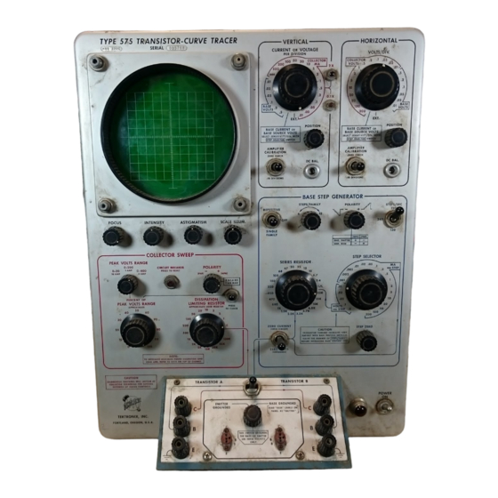
- Page 4 hokizoniai WTICM RANSIS OR-CUM RACfR VCKIJ O' O NltAlO* COUlClO* »* ,,r lU nK>Hix •* ---- ---------- - M...
- Page 5 SPEC F CAT ONS General Description Other Features Operating Specifications Collector Sweep Base Step Generator Mechanical Characteristics Vertical Display Accessories Horizontal Display @®...
- Page 6 NOTES...
- Page 7 COLLECTOR SWEEP Vertical Block Fig. 2-1. Type 575 front-panel layout. Each section corresponds to a block in the block diagram. EXT. ADAPTOR. SOCKET ---------- O TO 175 ADAPTOR. SOCKET EXT. Fig. 2-2. Type 575 functional block diagram. ®@l...
- Page 8 Operating nstructions — Type 575 Fig. 2-3. Function of front-panel vortical-block control*. Horizontal Block...
- Page 9 Operating nstructions — Type 575 Fig. 2-4. Function of front-panol horizontal-block confroll.
- Page 10 Operating nstructions — Type 575 Step Generator Block Transistor Test Panel transistor sockets only. Fig. 2-6. Function of base-step generator controls.
- Page 11 Operating nstructions — Type 575 2-7. Function of tott-panel controls. Setting Up The Front-Panel Controls Collector Sweep Block Base Step Generator Block General Procedure ndicator Unit Test Panel...
- Page 12 Operating nstructions — Type 575 Conclusion Testing a Transistor of Known Characteristics Test Panel Testing a Transistor of Unknown Characteristics 2. Collector Sweep Block Test Panel Collector Sweep Block Base Step Generator Block Base Step Generator Block ndicator Unit ndicator Unit...
- Page 13 Operating nstructions — Type 575 ■n ■ ■ a a* *i a i i a a a a a a • a a a a a tttt »" “ I TTTT I III TfTf Applying Voltage Steps to the Transistor nput Fig.
- Page 14 Operating nstructions — Type 575 Base Step Generator Block Characteristics of the Base Step Generator Functions of Controls and Switches Vertical Block Collector Sweep Block...
- Page 15 Operating nstructions — Type 575 Test Panel nterpreting Type 575 Curves Horizontal Block @®i...
- Page 16 Operating nstructions — Type 575 Collector Family Collector Family nverted Collector Family 2-10...
- Page 17 Operating nstructions — Type 575 Collector Family . . . Effect of collector to base capacity Horizontal Collector Sweep Amplifier Vertical Step Generator Amplifier Collector Family . . . External capacity added Collector Family . . . Saturation region 2-11...
- Page 18 Operating nstructions — Type 575 Collector Family . . . Room temperature (75° F.) -20v Collector Volts Above transistor at temperature of 150° F. 2-12...
- Page 19 Operating nstructions — Type 575 Breakdown Voltage, collector to emitter Collector Current l CE , l CEO , lets BV CE , BV CEO , BV , BV Breakdown Voltage, base to emitter Emitter Current l EO , Alpha Curve, a, h 21b , h fb , h PB...
- Page 20 Operating nstructions — Type 575 Forward Current Transfer Ratio, Beta, fj, h 21e , 1 OOma nput mpedance, h 11e , h ie 1 ma nput mpedance, h 11b , h ib -l-2ma Emitter Volts 2-14 'A A...
- Page 21 Operating nstructions — Type 575 Output Admittance, h 22b , h ob Collector-Base Volts Output Admittance, h 22e , h oe Voltage Feedback Ratio, - 50v Collector-Emitter Volts t _ - 0 02 ma. l.d xlC 08 ma. — 0.2v...
- Page 22 Operating nstructions — Type 575 Voltage Feedback Ratio, h 12b , h rb Collector-Base Volts +0.1v > — O.lv Reverse Transfer Resistance, r 12e — 2 ma 2-16...
- Page 23 Operating nstructions — Type 575 Output Resistance (input open-circuited to ac). -20ma Punch-Through Voltage (V ) and Floating Potential. Collector-Base Volts V PT '" Back-Biased NPN in Avalanche Mode Collector-Emitter Volts -f-5ma +50v @®1 2-17...
- Page 24 Operating nstructions — Type 575 Photodiode, with and without light Phototransistor, with and without light Tetrode NPN: Effect of nterBase Bias Collector Volts External Battery and Resistor 2-18...
- Page 25 Operating nstructions — Type 575 Zener or Reference Diode, Reverse Biased lOma Zener or Reference Diode, Forward Biased -|-1 Oma Voltage Regulator Tube NE-2 +2ma 2-19...
- Page 26 NOTES...
-
Page 27: Block Diagram
SECT ON 3 C RCU T DESCR PT ON Collector Sweep Block Diagram COLLECTOR SWEEP waveform Upper 120 position of STEPS/SEC switch STEP GENERATOR waveform Lower 120 position of STEPS/SEC switch 240 position of STEPS/SEC switch Fig. 3-1. The time relationship between waveforms of the Collector Sweep circuit and the Step Generator. - Page 28 Circuit Description — Type 575 Step Generator Staircase Generator Fig. 3-2. Basic circuit (a) for generating a step waveform (waveform B in (b).
- Page 29 Circuit Description — Type 575 SW TCH POS T ONS +300 V 23232 , 60v ..1.1 .I.. . -11 — I I 100V ___ / — -1.5V ----- S --------- K — 1.9V ------------- ------- ~ Fig. 3-3. The basic Miller...
-
Page 30: Pulse Generator
Circuit Description — Type 575 Fig. 3-4. Modification of Fig. 3-3. Pulse Generator Single-Family Triggering... - Page 31 Circuit Description — Type 575 Step Amplifier...
-
Page 32: Output Stage
Circuit Description — Type 575 Two 60 cycle sine waves, 90 degrees out of phase. V104A Cathode V124A Cathode V 12 ’ Full wave rectification of waveform A. Plate V132 Plate Full wave rectification of waveform B. Pulse generator output waveform Pulse repetition rate is 240/sec. - Page 33 Circuit Description — Type 575 t 150 V143A Cathode F 50 - ‘ 1.5 V172B Cathode V171 Grid -1.9 r 54 V163A Cathode V143B Cathode V155B Plate V152B Plate Fig. 3-7. Time relationships between Step Generator output waveforms and waveforms at key points in the step generator section.
- Page 34 Circuit Description — Type 575 Fig. 3-8. The Step Amplifier furnishes either current voltage steps to the input of the transistor under test. Fig. 3-11. Electron flow through the transistor V253 circuit when negative-going steps are required. Fig. 3-9. The emitter-follower (a) operates the same as the cath ...
- Page 35 Circuit Description — Type 575 Fig. 3-13. Simplified diagram of the Step Amplifier for negative-going current steps.
- Page 36 Circuit Description — Type 575 Fig. 3-14. Simplified diagram of the Step Amplifier for positive-going current steps. 3-10...
- Page 37 Circuit Description — Type 575 Collector MA Display Base Volts DISSIPA ION LIMI ING 1 VjDlV. 2 V/DIV. S vjDIV. CRT Deflection Amplifiers Fig. 3-15. With this configuration an accurate display of collector current (Vert. Amp.) and collector voltage (Horiz. Amp.) is ob ...
-
Page 38: Crt Circuit
Circuit Description — Type 575 CRT Circuit V657 , 3-12 ®@2... -
Page 39: Removal And Replacement Of Parts
ON 4 MA NTENANCE PREVENT VE MA NTENANCE Air Filter REMOVAL AND REPLACEMENT OF PARTS Removal of Panels Fan Motor Visual nspection Recalibration Fig. 4-1. Removal of the instrument side panels. -
Page 40: Replacement Parts
Maintenance — Type 575 Soldering Precautions Fig. 4-2 The method used to remove or replace the calhodc-ray tube. REPLACEMENT PARTS Replacement of Cathode-Ray Tube Standard Parts Replacement of Switches Special Parts Tube Replacement... -
Page 41: Troubleshoot Ng
Maintenance — Type 575 Parts Ordering nformation TROUBLESHOOT NG General nformation Circuit solation... - Page 42 Maintenance — Type 575 Troubleshooting The Low-Voltage Power Supply For no output voltage For failure of a power supply to regulate at the proper voltage Circuit Troubleshooting...
- Page 43 Maintenance — Type 575 Fig. 4-3. Chocking oporation of tho high voltage oscillator by tho placement of a neon bulb in tho field of the high voltage trans former. Troubleshooting the CRT Circuit Troubleshooting the Horizontal Amplifier...
- Page 44 Maintenance — Type 575 Troubleshooting the Step Generator Troubleshooting the Vertical Amplifier Pulse Generator ®®>...
- Page 45 Maintenance — Type 575 Stairstep Generator Adjusting The Step Amplifier...
- Page 46 Maintenance — Type 575 Fig. 4-4. Grounding tho junction of rosittor* R251 and R246 to chock operation of tho Stop Ampllfior Circuit. R2 6 Troubleshooting the Collector Sweep Circuit...
- Page 47 Maintenance — Type 575 Fig. 4*5. The waveform resulting from a failure of V733. This waveform shows collector current disployed vertically and col lector voltage displayed horizontally. The CURRENT OR VOLTAGE PER D V S ON switch is in the .01...
- Page 48 NOTES...
- Page 49 ECTION 5 RECALIBRATION PROCEDURE NTRODUCT ON 3. Checking the Dissipation Limiting Resistor Switch 4. Power Supply 1. Checking the Step Selector Switch 2. Checking the Series Resistor Switch...
- Page 50 Recalibration — Type 575 5. DC Balance 7. CRT Alignment CRT Adjustment S/N 101-1620 CRT Adjustment S/N 1620-up 6. Differential Balance 8. Vertical Gain Vertical Amplifier to a value which results in a trace de ...
- Page 51 Recalibration — Type 575 10. Phase A, Phase B, and Geometry 9. Horizontal Gain Fig. 5-1. Typical display resulting from proper adjustment of the Phase B control.
- Page 52 Recalibration — Type 575 12. Adjusting the Collector Sweep Balance Fig. 5-2. Typical display resulting from the proper adjustment of the Phase A control. 13. Min. No. Steps and Max. No. Steps 11. Zero Adj, ± Adj, and Volts/Step Adj 14.
- Page 53 Recalibration — Type 575 15. Checking Vertical Collector ma/div Switch...
- Page 54 Recalibration — Type 575 C706 Fig. 5-3 Left Side View...
- Page 55 Recalibration — Type 575 MAX. NO. STEPS VERT CAL M N. GA N ADJ. R334 HOR ZONTAL MAX. GA N ADJ. R434 VERT CAL MAX. GA N ADJ. Junction of R302 and R303 R359 R459 PHASE B C735 ZERO ADJ HOR ZONTAL M N.
- Page 56 NOTES...
- Page 57 SECT ON GENERAL DESCR PT ON Modification ACCESSOR ES Fig. 6-1. Location and dimensions of holes for mounting intercon necting plug in Type 575. Mounting NSTALLAT ON NSTRUCT ONS...
- Page 58 — Type 175 VERT HOR Z 150V + 100V V163 Fig. 6-4. Replacing cabinet bolt* with hinge boll* in Type 575. Fig. 6-2. Wiring connection* to nterconnecting plug n Type 575 (schematic) . OPERAT NG NSTRUCT ONS Fig. 6-3. Wiring connections to interconnecting plug in Type 575...
- Page 59 — Type 175 COLLECTOR SWEEP Block nterconnecting 10-32 x 1 bolt Power cable BASE STEP GENERATOR Block and nut (2) (Type 175 to Type 575) Fig. 6-5. Typo 575 tllt-mountod on Typo 175. Transistor Test Panel VERT CAL D SPLAY Switch...
- Page 60 Circuit Description — Type 175 C RCU T DESCR PT ON Block Diagram Step Amplifier Collector Sweep MA NTENANCE Troubleshooting the Step Amplifier...
- Page 62 + 300V + EXTERNAL HOR ZONTAL T° — EXTERNAL HOR ZONTAL J r-- -> + EXTERNAL VERT CAL ----- 5-Tn-> - EXTERNAL VERT CAL FROM STEP GEN (V 63, P N 3) TYPE 575 ----- ► NTERCONNECT NG CABLE...
- Page 63 Maintenance — Type 175 Troubleshooting the Collector Sweep Circuit HOR ZONTAL D SPLAY and STEP SELECTOR Switches. Checking Switch Resistance ®2...
- Page 64 Maintenance — Type 175 HOR ZONTAL D SPLAY Switch (COLLECTOR V ce Posi tions) VERT CAL D SPLAY Switch. ®i...
- Page 65 Calibration — Type 175 0.05 ft 0.05 ft SER ES RES STANCE switch. ZERO ADJ. CAL BRAT ON ADJ. Fig. 6-7. Bottom of Typo 175, showing internal adjuttmentt.
-
Page 66: Calibration - Type
Calibration — Type 175... - Page 67 ABBREV AT ONS SPEC AL NOTES AND SYMBOLS oe c1 '-'- oF CAT HOoe-^...
-
Page 68: How To Order Parts
HOW TO ORDER PARTS... - Page 69 PARTS L ST Type 575 Bulbs Capacitors /i/if /i/if 2000 /if 7/i/if 7/i/if 7 /i/if 7/i/if PARTS L ST — TYPE 575...
- Page 70 Capacitors (continued) fifif fifit Diodes Fuses PARTS L ST — TYPE 575...
- Page 71 Rectifiers Resistors ®®1 PARTS L ST — TYPE 575...
- Page 72 Resistors (continued) PARTS L ST — TYPE 575...
- Page 73 Resistors @©i PARTS L ST — TYPE 575...
- Page 74 Resistors (continued) @© PARTS L ST — TYPE 575...
- Page 75 Resistors (Cont'd) 301- 7 PARTS L ST — TYPE 575...
- Page 76 Resistors (continued) @© PARTS L ST — TYPE 575...
- Page 77 Resistors (continued) @®1 PARTS L ST — TYPE 575...
- Page 78 Resistors (continued) 50 n 8-10 PARTS L ST — TYPE 575...
- Page 79 Resistors (continued) Switches Thermal Cut-out Transformers 8-11 PARTS L ST — TYPE 575...
- Page 80 Electron Tubes Transistors 8-12 PARTS L ST — TYPE 575...
- Page 81 Mechanical Parts List Type 575 8-13 PARTS L ST — TYPE 575...
- Page 82 Mechanical Parts List (continued) 8-14 PARTS L ST — TYPE 575...
-
Page 83: Mechanical Parts List
Mechanical Parts List 8-15 PARTS L ST — TYPE 575... - Page 84 Mechanical Parts List (continued) 8-16 PARTS L ST — TYPE 575...
- Page 85 Mechanical Parts List (continued) 8-17 PARTS L ST — TYPE 575...
- Page 86 Mechanical Parts List (continued) Tektronix Part Number 8-18 PARTS L ST — TYPE 575...
- Page 87 PARTS L ST Type 175 Bulbs Capacitors Fuses Resistors 8-19 PARTS L ST — TYPE 175...
- Page 88 Tektronix Resistors (continued) Part Number 500 a 250 a 25 a 0.5 a .5 a 30 a 8-20 PARTS LIS — YPE 175...
- Page 89 Resistors (continued) Diodes Transistors 8-21 ®0 PARTS L ST — TYPE 175...
- Page 90 Switches Thermal Cutout Transformers Electron Tubes 8-22 PARTS L ST — TYPE 175...
- Page 91 Type 175 Mechanical Parts List 8-23 PARTS L ST — TYPE 175...
- Page 92 Mechanical Parts List (continued) '/ x'/ 8-24 PARTS L ST — TYPE 175...
- Page 93 Mechanical Parts List (continued) 5- 0 x % 8-25 ®» PARTS L ST — TYPE 175...
- Page 94 Mechanical Parts List (continued) 8-26 PARTS L ST — TYPE 175...
- Page 95 Mechanical Parts List (continued) 8-27 PARTS L ST — TYPE 575...
- Page 96 DIAG. PHASE INVERTER WAV E f O RMS MiiLIStC 0' 'Ef'.S/FAMil Y RSPtT TiVE/SlN. SEE. PARTS L ST FOR EARL ER. VALUES SERiAL NUMBER RANGELS PARTS MARKED WERE OBTA NED W TH BLUE OUTL NE. TYPE 575 TRANS STOR-CURVE TRACER...
- Page 97 DISCONNECT DIODES SCHMITT TRIGGER MILLER INTEGRATOR + 300V + 3oov V 63A V26AN8 CLAMP T BE R N P CF + 100V + 300V V152A STEP WAVEFORM V26AL5 . TO GRID, PIN 1 V214 THR (STEP AMP. DIAG.I MILLER V163B R N P 'A6ANB T BE...
- Page 98 REPET T VE/S NGLE FAM LY ... REPET T VE POLAR TY ............. _ STEPS/FAM LY ........... FULL R GHT STEP ZERO ........... FULL R GHT STEP SELECTOR ........... 0.2V/STEP V233B> 7 2 I2AU7 — 1.5 R273 R.274 R.27S TYPE 575 TRANS STOR-CURVE TRACER...
- Page 99 DRIVER. OF AMPLIFIER. PARTS LIST FOR EARLIER ES AND SERIAL MBER RANGES OF PARTS MARKED WITH TLINE.
- Page 100 AMPLIF1E...
- Page 101 SECOND AMPLIFIER AMPLIFIER AMPLIFIER + 3OOV + BOOV V4&4B 5W44O R453 %>6CG7 |47OKl AMPLIFIER R4&I ALIBR AT1ON 112-OKi 7 6AU6 R454 R47O ZOOK + 52 PPER DEFLECTION PLATE V45'7- R49O /2AJ6 BOOK + IOOV R448 + IOOV R457 + IOOV MAX.
- Page 102 POLAR TY ............— D SS PAT ON L M T NG RES STOR ..100 CURRENT OR VOLTAGE/D V ..... 1 00 MA TRANS STOR SELECTOR ......TRANS STOR TERM NAL C ..........GROUNDED 575 COLL- SWP. A&2...
- Page 103 ---------------- 1 ----------------- polaritv M LL SEC M LL SEC JTA NED .. 117 VAC .. 0-20 . . FULL R GHT • ■ + ■ . . 0 . . OFF . 117 VAC . 0-200 . 70 .100 .
- Page 104 TYPE TRANSISTOR-C TRACER...
- Page 105 ^AMPL F ER VERTICAL AMPLIFIER SWITCHING ---------- HOR ZONTAL NPUT NPUT TO GR D TO CATH. CAL BRAT ON TO GR D P N , V454 P L T? V454- — -| SOURCE — P N , V344 5W44O SW34O AMPL F ER CAL BRAT ON]"...
- Page 106 + 3OOV PRIMARIES CONNECTED FOR. 134VAC OptRATION T6OI TO + 3OOV FROM TERM. ZT 63VAC FROM TO V 602, V 607 ELEV. TO + 30 TO CRT HTR. ELEV. TO -1700 (SEE CRT C RCU 1 TO POWER SUPPLY HTRS. GND.
- Page 107 MECTED LR.ATION TGOl 1OLLECTOR DiAG.) OLLE.CTOR L A T — TO COLLECTORS V243 , V253 ,0241 “ Xo242 “ 1,0243 - 1 01.40 +J 1OOO X +~ 'LOOCyi.f ■ 20004^ +"T* 200QA/ - •it + STEP AMp. DIAGv + 100 C64I z LX2-O / u/ ‘...
- Page 108 OSC LLATOR + 4OOV NREG.. TYPE 575 TRAN5 5TOR-CURVE TRACER...
- Page 109 2-3N Z2e«a a-3N 929*9 kN«S*l t-zsa | IAI < 5IXVN^I±SV~| AOOI+ oze* +• aooi NG'S ©i©a *OOI •rav no2H> AOOll- AOOC+ 1091 0093 + ZI&A...
- Page 110 SET AS FOLLOWS. L NE VOLTAGE ..................117V AC STEPS/5EC (TYPE 575) ..............REPET T VE/S NGLE FAM LY (TYPE 575} ........REPET T VE STEPS/FAM LY (TYPE 575} ............... FULLY CW BASE STEP GEN. POLAR TY (TYPE 175) .........
- Page 111 SWITCHING DIAGRAM + 3OOV ei64 (500 KJ + 45 + IOOV SW2.44 STEP ._C267 BT-GG. SELECTOR .OOI N£- 2. J2.Z&7 — ■ R168 IOOR :RZ73 < RZ6S + IOOV >47K -I5OV RRENT + IOOV -l&OV R2.74 TRANSISTOR SELECTOR SWITCH SW5IO...
- Page 112 — J — w\ — !■ ------ O R244J R245J R41 5J R244K R245L R4ISK R244L R4I5L R2.44M E> TO GRID OF V444 OF TYPE- 575 R2.44N PIN ON CONNECTOR TO TYPE 575 (COLLECTOR swp. C R2-44P R. 2x440 ZERO CR246 >.478 RRENT TO C...
- Page 113 RRENT/DlV. 4F^R irtR VOLTS/DIV. TO R74O TO C RRENT-SWITCHING (COLLECTOR RELAYS SW731 SW73G SWP. DIAG.) (COLLECTOR SWR DIAG.) PINS ON CONNECTOR ---------- TO TYPE 575 ------------ (COLLECTOR SWp. DIAG.) R3IG& R4IBB M AMPS =» R3ISC R4I'=»C R31GC 3.37< 3.37R R4IBP RSIfeD %.64K...
- Page 114 234 VAC 117 VAC PRIMARY CONNECTIONS FOR 234VOLT OPERATION TYPE 175 TRANS STOR-CURVE TRACER H GH-CURRENT ADAPTOR...
- Page 115 + 300...
- Page 116 MANUAL CHANGE NFORMAT ON...
-
Page 118: Section 1 Specifications
TYPE 575 SECTION 1 SPECIFICATIONS Base Step Generator (Page 1-1, Paragraph 5) CHANGE TO: 5 voltage-step ranges from .01 volt/step to .2 volt/step ±5$, with output impedance adjustable from 1 ohm to 22 thousand ohms ±10$, plus 0.1 ohm (wiring and switch contact resistance). - Page 119 Type 175 Tent. S/N 570 PARTS LIST CORRECTION Change to: 2N21 8 Q233 151-0137-00 M O, 298/1165...
- Page 120 S L CON RECT F ER For Tektronix Type 575 Transistor-Curve Tracer Serial numbers 101-4929 DESCRIPTION This modification replaces the selenium rectifiers with silicon rectifiers. Silicon rectifiers offer more reliability and longer life. The following selenium rectifiers are replaced: SR241 (part number 106-0043-00);...
-
Page 121: Parts List
PARTS LIST Description Quantity Part Number 1 ea Assembly, silicon rectifier, consisting of: 2 ea Strip, cer, 3/4 x 7 notches, clip-mounted 124-0089-00 6 ea Diode, silicon, 500-750 mA 400 PIV 152-0066-00 2 ea Diode, silicon 15 A 100 PIV 152-0088-00 2 ea Fuse, w/pigtail,... - Page 122 INSTR CTIONS (cont) Wire the silicon rectifier assembly, as shown in Fig 2. Resolder the wires, unsoldered in step 3, to the thermal cutout. THIS COMPLETES THE INSTALLATION. Check wiring for accuracy. Replace the air filter, removed in step 1, and the fan assembly, displaced in step 2. Turn the instrument on and check the power supplies for proper voltages and regulation.
- Page 123 INSTR CTIONS (cont) ---- uu-gn P-2AO ---- UJ-bK — uj-bn uu-y uj-r «JU-O DfeZOC uu-y 040-0223-00 Page 4 of 4...
-
Page 124: General Information
S L CON RECT F ER Type 575 -- s/n 101-4929 Installed in Type 575 s/n _______ .Date _____ GENERAL INFORMATION This modification replaces the selenium rectifiers with silicon rectifiers. Silicon rectifiers offer more reliability and longer life. ELECTRICAL PARTS LIST Only new parts listed.
Need help?
Do you have a question about the 575 and is the answer not in the manual?
Questions and answers