
Subscribe to Our Youtube Channel
Related Manuals for Aiwa XD-DV487


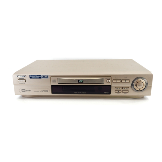
Summary of Contents for Aiwa XD-DV487
- Page 1 XD-DV487 EZ (B) XD-DV480 EZ (B) XD-DV480 EZ (NH) XD-DV480 K (NH) SERVICE MANUAL DVD PLAYER BASIC DVD/CD MECHANISM: DP-4RM S/M Code No. 09-01A-358-1N3...
-
Page 2: Table Of Contents
TABLE OF CONTENTS SPECIFICATIONS ................................... 3 PROTECTION OF EYES FROM LASER BEAM DURING SERVING .................... 4 ACCESSORIES LIST ..................................5 DISASSEMBLY INSTRUCTIONS ............................. 6 ~ 7 ELECTRICAL MAIN PARTS LIST ............................8 ~ 21 TRANSISTOR ILLUSTRATION ..............................22 BLOCK DIAGRAM - 1 (OVERALL) ............................... 23 BLOCK DIAGRAM - 2 (POWER) .............................. -
Page 3: Specifications
SPECIFICATIONS Audio output Digital output Power supply 230 V AC, 50 Hz 0.5 Vp-p (75 ohms) Power consumption 16 W Power consumption 1 Fiber optical connector in standby mode 2.9 W 1 RCA jack Weight 2.9 kg (7.1 lbs) Analog output External dimensions 430 ×... -
Page 4: Protection Of Eyes From Laser Beam During Serving
PROTECTION OF EYES FROM LASER BEAM DURING SERVICING CAUTION This set employs laser. Therefore, be sure to follow carefully the instructions below when servicing. Use of controls or adjustments or performance of proce- dures other than those specified herin may result in WARNING! hazardous radiation exposure. -
Page 5: Accessories List
ACCESSORIES PARTS LIST -1/1 = ! SAFTY PARTS = Components marked All components used on this model at the production line are shown in this service manual. However, please note that not all components will be available as spare parts for after-sales service. Components marked S and O are designated as spare parts for service and will be stocked at the spare parts centers. -
Page 6: Disassembly Instructions
DISASSEMBLY -1/2 CABINET DISASSEMBLY 1. Top Case 3. Front Panel 1. Release 7 screws (A). (See Fig. 2-1) 1. Eject the disc tray. (See Fig. 2-2) 2. Lift the top case with holding the back of it, 2. Remove the tray door. (See Fig. 2-2) and remove it in the direction of the arrow 3. - Page 7 DISASSEMBLY -2/2 CIRCUIT BOARD DISASSEMBLY 1. Disassembling of Main Circuit Board 2. Key and Power Led Circuit Board and Interface Board 1. Remove the front panel.(See Fig. 2-3) 2. Release 5 screws (E), remove the Key and 1. Remove the top case.(See Fig. 2-1) Power Led circuit board.
-
Page 8: Electrical Main Parts List
ELECTRICAL PARTS LIST - 1/14 = ! SAFTY PARTS = Components marked All components used on this model at the production line are shown in this service manual. However, please note that not all components will be available as spare parts for after-sales service. Components marked S and O are designated as spare parts for service and will be stocked at the spare parts centers. - Page 9 ELECTRICAL PARTS LIST - 2/14 = ! SAFTY PARTS = Components marked All components used on this model at the production line are shown in this service manual. However, please note that not all components will be available as spare parts for after-sales service. Components marked S and O are designated as spare parts for service and will be stocked at the spare parts centers.
- Page 10 ELECTRICAL PARTS LIST - 3/14 = ! SAFTY PARTS = Components marked All components used on this model at the production line are shown in this service manual. However, please note that not all components will be available as spare parts for after-sales service. Components marked S and O are designated as spare parts for service and will be stocked at the spare parts centers.
- Page 11 ELECTRICAL PARTS LIST - 4/14 = ! SAFTY PARTS = Components marked All components used on this model at the production line are shown in this service manual. However, please note that not all components will be available as spare parts for after-sales service. Components marked S and O are designated as spare parts for service and will be stocked at the spare parts centers.
- Page 12 ELECTRICAL PARTS LIST - 5/14 = ! SAFTY PARTS = Components marked All components used on this model at the production line are shown in this service manual. However, please note that not all components will be available as spare parts for after-sales service. Components marked S and O are designated as spare parts for service and will be stocked at the spare parts centers.
- Page 13 ELECTRICAL PARTS LIST - 6/14 = ! SAFTY PARTS = Components marked All components used on this model at the production line are shown in this service manual. However, please note that not all components will be available as spare parts for after-sales service. Components marked S and O are designated as spare parts for service and will be stocked at the spare parts centers.
- Page 14 ELECTRICAL PARTS LIST - 7/14 = ! SAFTY PARTS = Components marked All components used on this model at the production line are shown in this service manual. However, please note that not all components will be available as spare parts for after-sales service. Components marked S and O are designated as spare parts for service and will be stocked at the spare parts centers.
- Page 15 ELECTRICAL PARTS LIST - 8/14 = ! SAFTY PARTS = Components marked All components used on this model at the production line are shown in this service manual. However, please note that not all components will be available as spare parts for after-sales service. Components marked S and O are designated as spare parts for service and will be stocked at the spare parts centers.
- Page 16 ELECTRICAL PARTS LIST - 9/14 = ! SAFTY PARTS = Components marked All components used on this model at the production line are shown in this service manual. However, please note that not all components will be available as spare parts for after-sales service. Components marked S and O are designated as spare parts for service and will be stocked at the spare parts centers.
- Page 17 ELECTRICAL PARTS LIST - 10/14 = ! SAFTY PARTS = Components marked All components used on this model at the production line are shown in this service manual. However, please note that not all components will be available as spare parts for after-sales service. Components marked S and O are designated as spare parts for service and will be stocked at the spare parts centers.
- Page 18 ELECTRICAL PARTS LIST - 11/14 = ! SAFTY PARTS = Components marked All components used on this model at the production line are shown in this service manual. However, please note that not all components will be available as spare parts for after-sales service. Components marked S and O are designated as spare parts for service and will be stocked at the spare parts centers.
- Page 19 ELECTRICAL PARTS LIST - 12/14 = ! SAFTY PARTS = Components marked All components used on this model at the production line are shown in this service manual. However, please note that not all components will be available as spare parts for after-sales service. Components marked S and O are designated as spare parts for service and will be stocked at the spare parts centers.
- Page 20 ELECTRICAL PARTS LIST - 13/14 = ! SAFTY PARTS = Components marked All components used on this model at the production line are shown in this service manual. However, please note that not all components will be available as spare parts for after-sales service. Components marked S and O are designated as spare parts for service and will be stocked at the spare parts centers.
- Page 21 ELECTRICAL PARTS LIST - 14/14 = ! SAFTY PARTS = Components marked All components used on this model at the production line are shown in this service manual. However, please note that not all components will be available as spare parts for after-sales service. Components marked S and O are designated as spare parts for service and will be stocked at the spare parts centers.
-
Page 22: Transistor Illustration
• Regarding connectors, they are not stocked as they are not the initial order items. The connectors are available after they are supplied from connector manufacturers upon the order is received. CHIP RESISTOR PART CODE Chip Resistor Part Coding Figure Resistor Code Value of resistor Chip resistor... -
Page 23: Block Diagram - 1 (Overall)
BLOCK DIAGRAM -1/6 (OVERALL SECTION) DISC DVD_LDQM,DVD_SD,CSI IC302 MIRR,TZC DVD_MA[0:11] IC205 M12L16161A-7T DRAM 1M x 16bit AS4LC256K16E0-35 SDRAM IC2A1 DVD_MD[0:15] 256K x 16bit FE,TE,RFRP,SBADD,DVD/CD RF SSI33P3721 CD,DVD:A,B,C,D,E,F RF Signal PICK SPINDLE Processor TEBAL,FEBAL, DVD_SD_CAS, MOTOR DPOCTL,EQF,EQB DVD_SD_RAS DVD_SD_CLK IC303 DVD_MWE M12L16161A-7T Focus, tracking sled 1M x 16bit... -
Page 24: Block Diagram - 2 (Power)
BLOCK DIAGRAM -2/6 (POWER SECTION) RECTIFIER(FLD) D107,D108 -24VA RECTIFIER(14V) 12VA C126,C127, D110 L102 REG(8V) RECTIFIER(9V) IC105 C116 D106 KA78R08 5.2VA Q107 RECTIFIER(5.2V) 5V_D C124,C125, D109 L103 Q108 5V_A D114 D115 2.5V FEED B. D112 IC102 LTV-817B REG(3.3V) IC106 KA78R33TU REG(3.3V) 3.3V_M IC107 KA78R33TU... -
Page 25: Block Diagram - 3 (Rf/Cd Dsp/Dvd)
BLOCK DIAGRAM -3/6 (RF/CD, DSP/DVD SECTION) IC204 IC2A2 KIC7W53FU NJM3414AM-TE1 IC201 SBADD GDC25D801D CD/DVD DSP DVD SERVO SENS,FOK, 70,78, MSDATO,DEFECT,DSP_SENSE 131,132, DVD:A,B,C,D, SQSO,SQCK 114,118 PICK FE,TE,PI 11-16 XLAT,S_CLK,S_DATA 101, CD:A,B,C,D/E,F 80-82 DSP_CS,/WR,/RD IC2A1 MAIN -COM 175-177 DVD/CD RF SECTION SSI33P3721 DO[0:7] 185-193 RF Signal... -
Page 26: Block Diagram - 4 (Audio)
BLOCK DIAGRAM -4/6 (AUDIO SECTION) DAC_RST S_DATA MAIN -COM SECTION S_CLK DAC_L0 IC402 IC401 LPF &Buffer PCM1716E NJM4580D Audio DAC OP AMP DA_LRCK DA_BCK MPEG SECTION DA_XCK DA_DATA0 JACK SECTION <487> IC452 LPF &Buffer NJM4580D DAC_RST OP AMP S_DATA MAIN -COM S_CLK SECTION DAC_L1... -
Page 27: Block Diagram - 5 (Mpeg)
BLOCK DIAGRAM -5/6 (MPEG SECTION) DA_BCK,DA_XCK,DA_LRCK 122,125,126 AUDIO DA_DATA[0:3] SECTION 118-121 IC305 TC7W04FU Q303 DVD_DATA[0:7] COAXIAK JK601 SDCLK1,ZISENB DVD DSP 171, SPDIF OPTICAL DIGITAL SECTION REQZ1 IC301 ZiVA4.1B0 CVBS CVBS MPEG A/V A[00:02] Decoder CVBS/G D[00:07] MAIN SW602 Y(G) JK602 -COM V.SWITCH MPEG_ERROR... -
Page 28: Block Diagram - 6 (Μ-Com)
BLOCK DIAGRAM -6/6 (µ-COM SECTION) LD_ON,LOAD CTL,ACT_MUTE 16:9,SYSTEM_SW PI,SPINDLE_FG JACK DRIVE & RF SECTION SECTION MPEG DVD DSP D[00:07],A[00:02],S_CLK,S_DATA, SECTION SECTION D[00:07],A[00:05], ,E_SIN,E_CLK ,MPEG_INT,V_MUTE,DAC_RST LOCK,DEFECT,FOK,DSP_SENSE, SQCL,DSP_INT,/RD,1WR,DVD_DATA6 IIC_CLK IC504 ,IIC_DATA EEPROM MPEG_ERROR KS24C021CS ,DAC_L0 ,RF_LAT ,/DSP_CS IC505 D[00:07] DAC_RST ,/MPEG_CS MC74VHC374DTR2 SENS_MCOM ,E_DR ,/PP_CS, 16:9,... -
Page 29: Wire Harness Diagram
WIRE HARNESS DIAGRAM -1/1 P4301 P3401 C/R(B) CVBS/G(R) Y/B(G) A.GND CVBS V_MUTE 16:9 DOWNLOAD DAC_RST DAC_L0 DAC_L1 POWER S_CLK LED C.B S_DATA A.GND A.GND A.GND DA_BCK DA_DATA0 DA_DATA1 DA_DATA2 DA_DATA3 DA_LRCK DA_XCK 5V_A 5V_A A.GND A.GND KEY C.B A.GND A.GND A.GND DVD MECHA. -
Page 30: Schematic Diagram - 1 (Main - 1/4, Drive & Rf Section)
SCHEMATIC DIAGRAM - 1/9 (MAIN -1/4, DRIVE & RF SECTION) DVD MECHA. PICK UP MAIN-2/4 (DVD.DSP SECTION) MAIN-1/4 (DRIVE & RF SECTION) C.B 2A1-57 2A1-48 506-27 2A1-47 501-102 2A1-46 501-103 HB-1M2012-102JT MAIN-4/4 (MAIN -COM SECTION) 901-19 901-17 901-3 901-5 901-13 2A1-42 SSI33P3721 2A1-41... -
Page 31: Schematic Diagram - 2 (Main - 2/4, Dvd Dsp Section)
SCHEMATIC DIAGRAM - 2/9 (MAIN -2/4, DVD DSP SECTION) MAIN-2/4 (DVD DSP SECTION) C.B 201-177 506-8 201-178 501-23 201-179 501-24 201-180 501-25 201-181 501-26 201-182 501-27 201-183 501-28 201-185 501-4 IC205 201-187 501-5 AS4LC256K16E0-35 201-188 501-6 DRAM 201-189 501-7 201-190 501-8 201-191 501-9... -
Page 32: Schematic Diagram - 3 (Main - 3/4, Mpeg Section)
SCHEMATIC DIAGRAM - 3/9 (MAIN -3/4, MPEG SECTION) MAIN-3/4 (MPEG SECTION) C.B L301-L304,L307-L311 HB : HB-1M2012-102JT C341 0.01UF C340 0.01UF INTERFACE-1/4 C.B (AUDIO SECTION) P4301 301-172 IC301 301-173 201-206 ZIVA_4.1B0 301-161 201-205 301-162 201-197 MPEG A/V 301-163 201-198 MAIN-2/4 DECODER 301-164 201-199 (DVD DSP... -
Page 33: Schematic Diagram - 4 (Main - 4/4, Main Μ-Com Section)
SCHEMATIC DIAGRAM - 4/9 (MAIN -4/4, MAIN µ-COM SECTION) MAIN-4/4 (MAIN -COM SECTION) C.B L501-L503,L505-L507 5901-17 HB : HB-1M2012-102JT 5901-19 5901-5 5901-11 5901-13 5901-15 5901-3 IC505 MC74VHC374DTR2 506-27 EXPANDER 505-15 AT49F8192A-90TC D03-1 506-13 M11B416256A-35J FLASH ROM D03-3 506-14 DRAM 2M1-11 501-100 D03-13 506-32... -
Page 34: Wiring - 1 (Main C.b) -Top View
WIRING - 1/5 (MAIN C.B) -Top View- MAIN C.B (Top view) To INTERFACE C.B To INTERFACE C.B C533 P4301 P9501 C2M2 C2M1 R537 L311 R569 R535 C2N2 R2P6 C526 C532 C531 C529 R582 R2A1 C2M5 R583 R584 C523 R589 C2A1 C534 R2C1 R593... -
Page 35: Wiring - 2 (Main C.b) -Bottom View
WIRING - 2/5 (MAIN C.B) -Bottom View- MAIN C.B (Bottom view) To MECHA To MECHA C2M4 C2D3 C536 C2M3 C2D4 C2D1 C2D2 C274 X201 C232 C281 C279 C280 -35-... -
Page 36: Schematic Diagram - 5 (Interface - 1/4, Audio Section)
SCHEMATIC DIAGRAM - 5/9 (INTERFACE -1/4, AUDIO SECTION) INTERFACE-1/4 (AUDIO SECTION) C.B 12V REG (2/3) (2/3) (2/3) AUDIO DAC (2/3) (2/3) (1/3) (2/3) (1/3) (1/3) <487> (1/3) (1/3) (1/3) MAIN-3/4 C.B (MPEG SECTION) P3401 AUDIO DAC(5.1CH) (3/3) (3/3) INTERFACE-3/4 (JACK SECTION) (3/3) (3/3) (3/3) -
Page 37: Schematic Diagram - 6 (Interface - 2/4, Front Control, Timer, Key, Power Led Section)
SCHEMATIC DIAGRAM - 6/9 (INTERFACE -2/4, FRONT CONTROL, KEY, POWER LED SECTION) POWER KEY C.B SW902 INTERFACE -2/4(FRONT CONTROL SECTION) C.B OPEN/CLOSE LED C.B 7-BT-273GNS SW906 SW908 SW904 SW903 SW910,LED901 STOP PLAY PAUSE POWER SW905 SW907 R944 VCC2 MENU RESET TSOP2838WE1 (REMOCON RECEIVE) R943... -
Page 38: Schematic Diagram - 7 (Interface - 3/4, Jack Section) <487
SCHEMATIC DIAGRAM - 7/9 (INTERFACE -3/4, JACK SECTION) <487> JK603 TO TV 5.1CH AUDIO OUT AUDIO S-VIDEO OUT1 REAR FRONT DIGITAL VIDEO WOOFER CENTER INTERFACE-3/4 (JACK SECTION) C.B <487> L604 L603 DIGITAL AUTO NTSC GDZJ5.6B GDZJ5.6B GDZJ5.6B GDZJ5.6B GDZJ5.6B (3/3) (3/3) (3/3) (3/3) -
Page 39: Schematic Diagram - 8 (Interface - 3/4, Jack Section) <480
SCHEMATIC DIAGRAM - 8/9 (INTERFACE -3/4, JACK SECTION) <480> JK603 TO TV AUDIO AUDIO S-VIDEO OUT1 OUT2 DIGITAL VIDEO INTERFACE-3/4 L604 L603 (JACK SECTION) C.B <480> DIGITAL AUTO NTSC GDZJ5.6B GDZJ5.6B GDZJ5.6B GDZJ5.6B GDZJ5.6B (3/3) (3/3) S-VIDEO GDZJ5.6B VIDEO SCART 12V_A INTERFACE-1/4 (AUDIO SECTION) -
Page 40: Schematic Diagram - 9 (Interface - 4/4, Power Section)
SCHEMATIC DIAGRAM - 9/9 (INTERFACE -4/4, POWER SECTION) INTERFACE-4/4 (POWER SECTION)C.B 1OSP07U UZ-3.3BSB (SUF4007) 3.3V REG IN OUT IN OUT 3.3V REG <EZ> FMB-G24H<KN> 8V REG IN OUT F104 5V SW 3.9K IC102 LTV-817B PHOT COUPLER POWER SW AC POWER CORD 110-240V 50/60Hz INTERFACE-2/4... -
Page 41: Wiring - 3 (Interface C.b) <487
WIRING - 3/5 (INTERFACE C.B) <487> SW602 JK602 INTERFACE C.B <487> VIDEO CENTER WOOFER S-VIDEO VIDEO OUTPUT FRONT REAR JK601 SCART SW601 AUDIO AC POWER CORD DIGITAL DIGITAL JK603 OUT1 110-240V AUTO 50/60Hz TO AV OPTICAL S-VIDEO COAXTAL NTSC 5.1CH AUDIO OUT E C B E C B B C E... - Page 42 WIRING - 4/5 (INTERFACE C.B) <480> JK602 INTERFACE C.B <480> SW602 VIDEO VIDEO S-VIDEO OUTPUT JK601 AUDIO SW601 SCART AUDIO OUT2 AC POWER CORD DIGITAL DIGITAL JK603 OUT1 110-240V AUTO 50/60Hz OPTICAL TO AV COAXTAL NTSC S-VIDEO E C B E C B B C E B C E...
-
Page 43: Wiring - 5 (Key, Power Led C.b)
WIRING - 5/5 (KEY, POWER LED C.B) To POWER, A/V, FRONT C.B P9904 SW904 SW903 SW902 KEY C.B STOP PLAY OPEN/CLOSE SW912 SW906 SW905 SW911 SW910 SW913 SW907 SW908 ENTER MENU PAUSE SW914 To INTERFACE C.B P9902 POWER LED C.B SW901,LED901 POWER STANDBY/ON... -
Page 44: Waveforms - 1/2
WAVEFORMS - 1/2 IC301 (MPEG) 3 IC301 Pin 145 Luminance 1 IC301 Pin 133 Composite 2 IC301 Pin 151 Chrominance (Super video out Mode) 500mV/20µs (Super video out Mode) 500mV/20µs 500mV/20µs M 500 s 280/mV 1.00V IC301 Pin 159 MPEG Clock (27MHz) IC301 Pin 145 Component Pb 6 IC301 Pin 151 Component Pr 1.0V/500µs... - Page 45 WAVEFORMS - 2/2 IC2A1, IC201 (DRIVE/RF, DVD DSP) IC2A1 Pin 42 Focus Error IC2A1 Pin41 Tracing Error IC2A1 Pin41 VBR Tracking Error IC2A1 Pin 36 Pi 500mV/2ms 500mV/300µs 500mV/5ms IC2A1 Pin57 RF IC201 Pin88 SLED Driver (FMO) IC2A1 Pin42 Focus Error(in Focus Search) 0.5V/0.1µs IC201 Pin18 SLED FG IC201 Pin83 Focus Drive (FDO)
-
Page 46: Voltage Chart
VOLTAGE CHART - 1/7 (DSP SECTION) IC201 GDC25D801D IC205 AS4LC256K16E MODE MODE MODE MODE MODE PLAY PLAY PLAY PLAY PLAY PIN NO. PIN NO. PIN NO. PIN NO. PIN NO. 3.16 3.18 2.00 1.30 5.00 4.98 3.25 4.20 3.10 2.50 2.01 2.07 2.00... - Page 47 VOLTAGE CHART - 2/7 (SERVO SECTION) IC2M1 FAN8727 IC2A1 SSI33P3721 MODE MODE MODE PLAY PLAY PLAY PIN NO. PIN NO. PIN NO. 5.02 0.80 3.44 3.38 3.71 3.70 5.01 2.48 3.12 3.40 3.75 3.70 2.08 2.07 2.50 2.50 0.27 0.36 2.12 1.95 2.51...
- Page 48 VOLTAGE CHART -3/7 (MPEG SECTION-1/2) IC302 M12L16161A-7T IC301 ZIVA4.1B0 MODE MODE MODE MODE MODE PLAY PLAY PLAY PLAY PLAY PIN NO. PIN NO. PIN NO. PIN NO. PIN NO. 3.13 3.10 0.90 1.20 0.00 1.60 3.12 0.00 3.15 3.10 0.15 0.20 1.20 1.50...
- Page 49 VOLTAGE CHART - 4/7 (MPEG SECTION-2/2) IC304 TC7W04FU IC303 M12L16161A-7T MODE MODE PLAY PLAY PIN NO. PIN NO. 2.67 2.76 3.15 3.10 2.76 2.76 0.65 1.20 2.76 2.76 0.70 1.20 0.00 0.00 0.00 0.00 2.22 2.21 0.92 1.10 2.23 2.22 0.77 1.10 2.23...
- Page 50 VOLTAGE CHART -5/7 (SYSTEM SECTION-1/2) IC503 M11B416256A IC505 MC74VHC374 IC501 HD6417034AF112 IC502 AT49F8192A MODE MODE MODE MODE MODE PLAY PLAY PLAY PLAY PLAY PIN NO. PIN NO. PIN NO. PIN NO. PIN NO. 0.00 0.00 4.98 4.96 0.50 0.90 0.00 0.00 0.00 0.00...
- Page 51 VOLTAGE CHART - 6/7 (SYSTEM-2/2, FRONT, JACK SECTION) IC901 PD 780232GC IC506 HS602002 IC902 KIA7042P MODE MODE MODE MODE PLAY PLAY PLAY PLAY PIN NO. PIN NO. PIN NO. PIN NO. -20.40 -20.00 0.00 0.00 5.00 5.01 5.09 5.00 -16.90 -16.90 5.00 4.98...
- Page 52 VOLTAGE CHART - 7/7 (AUDIO, POWER SECTION) IC401 PCM1716E IC451 PCM1601Y IC101 KA5M0365R IC452 NJM4580D MODE MODE MODE MODE PLAY PLAY PLAY PLAY PIN NO. PIN NO. PIN NO. PIN NO. 1.60 1.59 0.00 0.00 5.36 5.38 0.00 0.00 0.00 1.61 5.37 5.37...
-
Page 53: Lcd Display - 1/1
LCD DISPLAY - 1/1 TITLE CHP/TRK PROG.NKS RANDOM ALL A DVD A col2 col1 9 10 11 12 13 14 15 16 17 18 19 20 21 22 23 24 25 26 27 28 29 30 31 32 33 34 35 36 37 38 39 40 41 42 .... -
Page 54: Ic Block Diagram
IC BLOCK DIAGRAM -1/4 IC, PCM1716E BCKIN Low-pass Serial Filter LRCIN Input EXTL 8X Oversampling Enhanced Digital Filter with Multi-level Function Delta-Sigma Controller Modulator Low-pass Filter ML/IIS EXTR MC/DM1 MD/DM0 ZERO Mode CS/IWO Control BPZ-Cont. Open Drain MODE MUTE Crystal/OSC Power Supply CLKO AGND1... - Page 55 IC BLOCK DIAGRAM -2/4 IC, AS4LC256K16EO-35 UCAS LCAS RAS CLOCK CAS CLOCK WE CLOCK OE CLOCK GENERATOR GENERATOR GENERATOR GENERATOR Data I/O BUS I/O1 I/O2 COLUMN DECODERS I/O3 REFRESH I/O4 SENSE AMPLIFIERS BUFFER I/O5 COUNTER I/O6 I/O7 512 16 I/O8 I/O9 I/O10 I/O11...
- Page 56 IC BLOCK DIAGRAM -3/4 IC, XC9536-15VQ44C JTAG In-System Programming Controller JTAG Port Controller Function Block 1 Macrocells 1 to 18 Function Block 2 Macrocells 1 to 18 Blocks Function Block 3 Macrocells 1 to 18 I/O/GCK Function Block 4 I/O/GSR Macrocells I/O/GTS 1 to 18...
- Page 57 IC BLOCK DIAGRAM -4/4 IC, PCM1601Y Output Amp and Low-Pass Filter LRCK Output Amp and Audio Low-Pass Filter Serial DATA1 DATA2 Output Amp and Enhanced Oversampling DATA3 Low-Pass Filter Multi-level Digital Filter Delta-Sigma with Modulator Function Output Amp and Controller Low-Pass Filter TEST Serial...
- Page 58 IC DESCRIPTION - 1/9 (SSI33P3721)-1/2 Pin No. Pin Name Description DVDRFP RF SIGNAL INPUTS: Differential RF signal attenuator input pins. DVDRFN CD PHOTO DETECTOR INTERFACE INPUTS: Inputs from the CD photo detector outputs. PHOTO DETECTOR NTERFACE INPUTS: AC coupled inputs for the DPD from the main beam Photo detector matrix outputs.
- Page 59 IC DESCRIPTION - 1/9 (SSI33P3721)-2/2 Pin No. Pin Name Description PULL-IN SIGNAL OUTPUT: The summing signal output of A,B,C,D inputs for mirror detection. Reference to VCI. DEFECT OUTPUT: Pseudo CMOS output. When defect is detected, the DFT output goes high. Also the servo AGC output can be monitored at this DFT pin, when CAR bit7-4 is ‘0011’.
- Page 60 IC DESCRIPTION - 2/9 (AS4LC256K16EO-35)-1/1 Pin No. Pin Name Description – Power Supply (+3.3 V) 2 ~ 5 I/O1 ~ I/O4 Data-In / Data-Out – Power Supply (+3.3 V) 7 ~ 10 I/O5 ~ I/O8 Data-In / Data-Out 11, 12 –...
- Page 61 IC DESCRIPTION - 3/9 (M12L16161A-7T)-1/2 Pin No. Pin Name Description – 3.3 V is applied. (VCC is for the internal circuit.) Data is input and ouput from these pins. These pins are the same as those of a conventional DRAM. VSSQ –...
- Page 62 IC DESCRIPTION - 3/9 (M12L16161A-7T)-2/2 Pin No. Pin Name Description This pin determines whether or not the next CLK is valid. If CKE is High, the next CLK rising edge is valid. If CKE is Low, the next CLK rising edge is invalid. This pin is used for power- down and clock suspend modes.
- Page 63 IC DESCRIPTION - 4/9 (PCM1716E)-1/1 Pin No. Pin Name Description LRCIN Left and Right Clock Input. This clock is equal to the sampling rate - f .(1) Serial Audio Data Input. (1) BCKIN Bit Clock Input for Serial Audio Data.(1) CLKO Buffered Output of Oscillator.
- Page 64 IC DESCRIPTION - 5/9 (AT49F8192A-90TC)-1/1 Pin No. Pin Name Description 1 ~ 8 A16 ~ A9 Addresses Addresses – Not used _______ Write Enable ____________ RESET Reset 13 ~ 15 – Not used 16, 17 A18, A17 Addresses 18 ~ 25 A7 ~ A0 Addresses _____...
- Page 65 IC DESCRIPTION - 6/9 (GDC25D801D)-1/5 Pin No. Pin Name Description DAT1 Bi-directional data to DRAM DAT2 Bi-directional data to DRAM DAT3 Bi-directional data to DRAM DAT4 Bi-directional data to DRAM DAT5 Bi-directional data to DRAM DAT6 Bi-directional data to DRAM DAT7 Bi-directional data to DRAM DAT8...
-
Page 66: Ic Description
IC DESCRIPTION - 6/9 (GDC25D801D) - 2/5 Pin No. Pin Name Description TEST_OUT8 Test output TEST_OUT7 Test output TEST_OUT6 Test output T_SEL Test mode selection TEST_OUT5 Test output TEST_OUT4 Test output TEST_OUT3 Test output TEST_OUT2 Test output TEST_OUT1 Test output TEST_OUT0 Test output TEST_SEL0... - Page 67 IC DESCRIPTION - 6/9 (GDC25D801D) - 3/5 Pin No. Pin Name Description AVDD – Analog power supply for ADC AGND – Analog GND for ADC AOUT3 AOUT4 D_VREF DGND – Digital GND for ADC RFVCM – Analog GND for ADC AGND –...
- Page 68 IC DESCRIPTION - 6/9 (GDC25D801D) - 4/5 Pin No. Pin Name Description SI_ENC1 SLED ENCODER1 INPUT SI_ENC2 SLED ENCODER2 INPUT TRACK CROSS PULSE 2 INPUT MIRR TRACK CROSS PULSE 1 INPUT MSDATAO SERVO DSP INTENAL STATUS SERIAL OUTPUT INTERNAL GENERATED FOK(Focus OK) H=OK –...
- Page 69 IC DESCRIPTION - 6/9 (GDC25D801D) - 5/5 Pin No. Pin Name Description Spindle motor ON/OFF control signal LOCK CLV servo lock signal FG_M – Digital GND SCAN_OUT SCAN DATA OUTPUT (Not used) – Digital power supply Interrupt request to Host Read strobe from HOST Write strobe from HOST Chip select from HOST...
- Page 70 IC DESCRIPTION - 7/9 (HD6417034AF112) - 1/4 Pin No. Pin Name Description _____ IRQ6 Interrupt request 6. TP14 Timing pattern output 14. Timing pattern output pins. PB14 Port B: 16-bit input/output pins. Input or output can be selected individually for each bit. _____ IRQ7 Interrupt request 7.
- Page 71 IC DESCRIPTION - 7/9 (HD6417034AF112) - 2/4 Pin No. Pin Name Description _____ Wait. Requests the insertion of wait states (TW) into the bus cycle when the external address WAIT space is accessed. Chip select 7. Chip select signals for accessing external memory and devices. Port A.
- Page 72 IC DESCRIPTION - 7/9 (HD6417034AF112) - 3/4 Pin No. Pin Name Description System clock – Ground EXTAL External clock. XTAL Crystal. – Power. Nonmaskable interrupt. _________ WDTOVF Watchdog timer overflow. Overflow output signal from the watchdog timer. – Power. PROM programming power supply WDTOPVF –...
- Page 73 IC DESCRIPTION - 7/9 (HD6417034AF112) - 4/4 Pin No. Pin Name Description Timing pattern output 5. Timing pattern output pins. TIOCB4 ITU input capture/output compare (channel 4). Input capture or output compare pins. Port B: 16-bit input/output pins. Input or output can be selected individually for each bit. TOCXA4 ITU output compare (channel 4).
- Page 74 IC DESCRIPTION - 8/9 (µPD780232GC) - 1/1 Pin No. Pin Name Description VCC1 – Positive power supply except for ports, analog, and FIP controller/driver VSS1 – Ground potential except for ports and analog – Crystal connection for main system clock oscillation –...
- Page 75 IC DESCRIPTION - 9/9 (ZIVA4.1B0) - 1/5 Pin No. Pin Name Description _____ Read strobe in I mode. Must be held HIGH in M Mode. ____ Read/write strobe in M mode. Write strobe in I mode. Host asserts R/W LOW to select Write and ____ LOW to select Read for M Mode only.
- Page 76 IC DESCRIPTION - 9/9 (ZIVA4.1B0) - 2/5 Pin No. Pin Name Description 57 ~ 62 MDATA2 ~ MDATA7 SDRAM Data MDATA15 SDRAM Data VDD_3.3 – 3.3-V supply voltage for I/O signals. – Ground for core logic and I/O signals. MDATA14 SDRAM Data VDD_2.5 –...
- Page 77 IC DESCRIPTION - 9/9 (ZIVA4.1B0) - 3/5 Pin No. Pin Name Description DAI-DATA PCM data input. 118 ~ 121 DA-DATA3~ DA-DATAO PCM Data Out. Eight channels. Serial audio samples relative to DA_BCK and DA_LRCK. DA-LRCK PCM Left Clock. Identifies the channel for each sample. The polarity is programmable. VDD_3.3 –...
- Page 78 IC DESCRIPTION - 9/9 (ZIVA4.1B0) - 4/5 Pin No. Pin Name Description Video clock. Clocks out data on input. VDATA[7:0]. Clock is typically 27 MHz. VCLK System clock that drives internal PLLs and internal DENC. ZiVA-4 requires an external 27-MHz TTL oscillator.
- Page 79 IC DESCRIPTION - 9/9 (ZIVA4.1B0) - 5/5 Pin No. Pin Name Description VDD_2.5 – 2.5-V supply voltage for core logic. RESERVED Tie to VSS or VDD_3.3. – Ground for core logic and I/O signals. VDD_3.3 – 3.3-V supply voltage for I/O signals. 193 ~ 196 RESERVED Tie to VSS or VDD_3.3.
-
Page 80: Mechanical Exploded View 1/1
MECHANICAL EXPLODED VIEW 1/1 -80-... -
Page 81: Mechanical Main Parts List 1/1
MECHANICAL PARTS LIST -1/1 = ! SAFTY PARTS = Components marked All components used on this model at the production line are shown in this service manual. However, please note that not all components will be available as spare parts for after-sales service. Components marked S and O are designated as spare parts for service and will be stocked at the spare parts centers. -
Page 82: Color Name Table
COLOR NAME TABLE Basic color symbol Color Basic color symbol Color Basic color symbol Color Black Cream Orange Green Gray Blue Transparent Blue Gold Pink Silver Titan Silver Brown Violet White Transparent White Yellow Transparent Yellow Metallic Blue Light Blue Transparent Green Dark Blue Transparent Orange... -
Page 83: Dvd Mechanism Exploded View 1/1
DVD MECHANISM EXPLODED VIEW 1/1... -
Page 84: Dvd Mechanism Main Parts List 1/1
DVD MECHANISM PARTS LIST -1/1 = ! SAFTY PARTS = Components marked All components used on this model at the production line are shown in this service manual. However, please note that not all components will be available as spare parts for after-sales service. Components marked S and O are designated as spare parts for service and will be stocked at the spare parts centers. -
Page 85: Other Parts List 1/1
OTHER PARTS LIST -1/1 = ! SAFTY PARTS = Components marked All components used on this model at the production line are shown in this service manual. However, please note that not all components will be available as spare parts for after-sales service. Components marked S and O are designated as spare parts for service and will be stocked at the spare parts centers. -
Page 86: Electrical Troubleshooting Guide
ELECTRICAL TROUBLESHOOTING GUIDE -1/10 1. Power(SMPS) Circuit No 5V_D No VF+ or 5V_A . Is 5.2VA section working? Is 5.2VA section working? Is oscillation present at the Is oscillation present at the anode of D109? Base of Q108? No 5.2VA. Replace D109. - Page 87 ELECTRICAL TROUBLESHOOTING GUIDE -2/10 2. µ-COM Circuit A. No Power POWER ON Does Hellow appear at FLD? Is P5901 Does no DISC appear? connected normally? Reconnect it. Does Logo appear Check power. on the screen? (Refer to power) If power is normal Is P5901 Pin 23 normal? Refer to Front Part...
- Page 88 ELECTRICAL TROUBLESHOOTING GUIDE -3/10 B. Audio abnormal C. Video abnormal AUDIO ABNORMAL VIDEO ABNORMAL Check Audio jack. Check Video jack. YES (If OK) YES (If OK) Check MPEG_CLK Signal Refer to Video part. of MPEG part. YES (If OK) YES (If OK) Refer to Audio part.
- Page 89 ELECTRICAL TROUBLESHOOTING GUIDE -4/10 E. Picture abnormal PICTURE ABNORMAL Check the disc. Refer to Servo part If OK Check MPEG_CLK Signal of MPEG part YES (If OK) Check DSP YES (If OK) Check MPEG F. Disc Error DISC ERROR Check Disc YES (If OK) Refer to Servo part -89-...
- Page 90 ELECTRICAL TROUBLESHOOTING GUIDE -5/10 3. MPEG Circuit Power is on Does Logo appear Check power & clock. on the screen? Does the Check CD/DVD DSP output moving picture of the DVD Disc Is MPEG data signal normal? play on the screen signal.
- Page 91 ELECTRICAL TROUBLESHOOTING GUIDE -6/10 4. Front Circuit START Power on. Is oscillation of Check Power. LED ON? X901 normal? Check waveform Is Digitron on normally? Replace IC902. of IC901 Pin 6. Do all the Is waveform of IC901 Check waveform buttons work Pin 40 normal? of IC901 Pin 22.
- Page 92 ELECTRICAL TROUBLESHOOTING GUIDE -7/10 5. RF/Servo Circuit CHECK POINT(General) Does signal goes "High" to IC201 Pin194 when the power is on? Does signal pulse Check "2.µ-COM Part". input to IC201 Pins 58, 59 when the powe is on? Does Does Replace X301 or IC304 TTL pulse output to 33.8688MHz clock input...
- Page 93 ELECTRICAL TROUBLESHOOTING GUIDE -8/10 No disc .Power on Check loading Part. Push Pick-up to inner track to Does tray open or close? the end by hand. Does DECK assembly is defective. PMD03 Pin 13 change (Limit sw) high to low? Pressing the open/close key repeatedly, check the voltage of IC2M1...
- Page 94 ELECTRICAL TROUBLESHOOTING GUIDE -9/10 DISC IN OPEN/CLOSE Fig.3. FOCUS ERROR waveform Check Check IC2A1 Pin 11,12,13,14 the focus error moving the FOCUS ON? lens up and down. in DVD Mode (IC2A1 Pin 42) IC201 no output : Pick-up is defective. Does the TTL level change at IC201 Replace IC201.
- Page 95 ELECTRICAL TROUBLESHOOTING GUIDE -10/10 CHECK A Fig.5. RF waveform Check RF Eye-Pattern. No signal: Pick-up is defective Check IC2A1 Pins 5, 6, 7, 8. RF : 1.5-1.6V(IC2A1 Pin 57) Does the sawtooth waveform emit Is the eye-pattern vivid? Does the 1.6V emit? Replace IC2A1.
-
Page 96: Dvd Mechanism Parts Location
DVD MECHANISM PARTS LOCATION -1/1 • Top View (With Tray) Procedure Disass Fig- Parts Fixing Type embly Starting No. Holder 2 Screws, Clamp 2 Locking Tabs Clamp Assembly Disc 1, 2 Plate Clamp 1, 2, 3 Magnet Clamp 1, 2, 3, 4 Clamp Upper Tray Disc 1, 6... -
Page 97: Dvd Mechanism Disassembly
DVD MECHANISM DISASSEMBLY -1/3 HOLDER CLAMP PLATE CLAMP CLAMP ASSEMBLY DISC TRAY DISC MAGNET CLAMP CLAMP UPPER (S1) (S1) HOLDER CLAMP BASE MAIN (Fig. A) EMERGENCY EJECT HOLE BASE MAIN (L1) LEVER (L1) HOLDER CLAMP BASE MAIN BOTTOM SIDE VIEW Fig. - Page 98 DVD MECHANISM DISASSEMBLY -2/3 (L2) GEAR ASSEMBLY FEED GEAR MIDDLE (S2) GEAR ASSEMBLY RACK (S2) (S3) (S2) PICK UP ASSEMBLY GENERAL BASE PU(OUTSERT) (C1) (S2) RUBBER REAR GEAR ASSEMBLY FEED PICK UP ASSEMBLY GENERAL GEAR MIDDLE GAER ASSEMBLY RACK MOTOR ASSEMBLY SPINDLE MOTOR ASSEMBLY SPINDLE Fig.
- Page 99 DVD MECHANISM DISASSEMBLY -3/3 GUIDE UP/DOWN GEAR LOADING (L3) (L6) GEAR PULLEY (L6) (L4) BASE MAIN BELT LOADING (H1) PWB ASSEMBLY LOADING (L6) (S5) BASE MAIN FRAME ASSEMBLY UP/DOWN (S4) (L5) FIG. (A) GUIDE UP/DOWN FIG. (B) GUIDE UP/DOWN GUIDE UP/DOWN FIG.
- Page 100 DVD MECHANISM ADJUSTMENT -1/2 1. Tools and Fixtures for SVC • For SVC Program Down-Load Fig.1. Printer Cable Fig.2. FFC Cable (15 pin) Fig.3. Jig Board Fig.4. Deviation Disc (0.8mm) • For T-Skew and R-Skew Adjustment Fig.5. L-Wrench(3mm) Fig.6. RCA Jack Fig.7.
-
Page 101: Dvd Mechanism Adjustment- 2/2
DVD MECHANISM ADJUSTMENT- 2/2 CURRENT PICK UP POSITION ERROR RATE SIZE SECTOR : 200145 OR : 200145 ERROR RATE (HEXADEAMAL) 0045 0065 AVERAGE ERROR RATE Fig.11. Adjusting Screen Display 3. Adjustment Procedure 1. Insert Disc(Only Open/Close Key Pressing) 2. Wait Until the Sector Display is about 200,000 (Fig.11) 3. - Page 102 2–11, IKENOHATA 1–CHOME, TAITO-KU, TOKYO 110-8710, JAPAN TEL:03 (3827) 3111 0251431 Printed in Singapore...
Need help?
Do you have a question about the XD-DV487 and is the answer not in the manual?
Questions and answers