Table of Contents
Advertisement
Quick Links
Technical Explanation
SKYPER
®
1. Introduction ............................................................................................................................... 2
2. Block Diagram and Application Example ........................................................................................ 3
2.1 Block diagram ....................................................................................................................... 3
2.2 Application example .............................................................................................................. 4
2.2.1
Primary side ................................................................................................................... 4
2.2.2
Secondary side ............................................................................................................... 5
3. Dimensions and mechanical precautions ........................................................................................ 8
3.1 Dimensions .......................................................................................................................... 8
3.2 Plug-in connection ................................................................................................................. 8
3.3 Support post......................................................................................................................... 9
3.4 Solder connection .................................................................................................................. 9
3.5 Handling instructions ........................................................................................................... 10
4. Interface Description................................................................................................................. 11
4.1 Footprint ............................................................................................................................ 11
4.2 Pin assignment ................................................................................................................... 11
4.2.1
Pin assignment of pin header X10 | Primary side ............................................................... 11
4.2.2
Pin assignment of pin header X100 | Secondary side | TOP ................................................ 12
4.2.3
Pin assignment of pin header X200 | Secondary side | BOT ................................................ 12
4.3 Power Supply | Primary side ................................................................................................. 13
4.4 Gate drive signals | Primary side ........................................................................................... 14
4.5 Filter selection, jitter and propagation delay time | Primary side ............................................... 15
4.6 Error output | Primary side ................................................................................................... 15
4.7 Error input | Primary side ..................................................................................................... 16
4.8 Error mode selection | Primary side ....................................................................................... 17
4.9 External error input | Secondary side ..................................................................................... 17
4.10 Gate resistors | Secondary side ............................................................................................. 19
4.11 External boost capacitors | Secondary side ............................................................................. 20
5. Protection features ................................................................................................................... 21
5.1 Failure management ............................................................................................................ 21
5.2 Dead time and Interlock ....................................................................................................... 23
5.3 Short pulse suppression (SPS) .............................................................................................. 24
5.4 Undervoltage lockout (UVLO) ................................................................................................ 24
5.5.1
DSCP | Functional description ......................................................................................... 26
5.5.2
DSCP | Calculation hints ................................................................................................ 27
5.6 Active clamping................................................................................................................... 27
5.7 Soft Off .............................................................................................................................. 28
5.8 Safe short circuit turn-off in multilevel topology ...................................................................... 29
6. Electrical characteristic .............................................................................................................. 29
7. Product Qualification ................................................................................................................. 30
8. Environmental conditions .......................................................................................................... 31
9. Marking ................................................................................................................................... 32
10. Change history ......................................................................................................................... 33
© by SEMIKRON / 2019-07-23 / Technical Explanation / SKYPER
PROMGT.1026/ Rev.7/ Template Technical Explanation
Revision:
Issue date:
Prepared by:
Reviewed by:
Approved by:
Keyword: IGBT driver core
-monitoring (DSCP) .................................................... 25
®
42 LJ R
12
2019-07-23
Niklas Hofstötter
Daniel Obernöder
Marco Honsberg
Page 1/35
Advertisement
Table of Contents

Related Manuals for SEMIKRON SKYPER 42 LJ R


Summary of Contents for SEMIKRON SKYPER 42 LJ R
-
Page 1: Table Of Contents
7. Product Qualification ......................... 30 8. Environmental conditions ......................31 9. Marking ........................... 32 10. Change history ......................... 33 © by SEMIKRON / 2019-07-23 / Technical Explanation / SKYPER ® 42 LJ R Page 1/35 PROMGT.1026/ Rev.7/ Template Technical Explanation... -
Page 2: 42 Lj R
MTBF rate > 7.5 Million hours at full load Selectable error management modes for standard and multilevel applications © by SEMIKRON / 2019-07-23 / Technical Explanation / SKYPER ® 42 LJ R Page 2/35 PROMGT.1026/ Rev.7/ Template Technical Explanation... -
Page 3: Block Diagram And Application Example
Block Diagram and Application Example Block diagram Figure 2: SKYPER ® 42 LJ R | Block diagram © by SEMIKRON / 2019-07-23 / Technical Explanation / SKYPER ® 42 LJ R Page 3/35 PROMGT.1026/ Rev.7/ Template Technical Explanation... -
Page 4: Application Example
Figure 3 and Figure 4 show a typical SKYPER ® 42 LJ R core setting for operating a semiconductor module in half-bridge configuration. SEMIKRON’s highly-integrated ASICs – as utilized on this driver core – enable the SKYPER ® 42 LJ R to be easily configured with only a few simple external circuits and in turn reducing the project and development time as well as the cost. -
Page 5: Secondary Side
X100:01 CLMP_IN_TOP X100:07 PWR_GND_TOP X100:08 PWR_VS_N_TOP X100:10 PWR_VS_P_BOT X200:03 nERR_IN_BOT X200:04 CFG_VCE_BOT X200:01 CLMP_IN_BOT X200:07 PWR_GND_BOT X200:08 PWR_VS_N_BOT X200:10 © by SEMIKRON / 2019-07-23 / Technical Explanation / SKYPER ® 42 LJ R Page 5/35 PROMGT.1026/ Rev.7/ Template Technical Explanation... - Page 6 Dimensioning according to G(softoff)_BOT chapter 4.10. Optional series resistor for V -monitoring, mandatory if 511Ω VCE_TOP VCE_BOT DSCP is used. © by SEMIKRON / 2019-07-23 / Technical Explanation / SKYPER ® 42 LJ R Page 6/35 PROMGT.1026/ Rev.7/ Template Technical Explanation...
- Page 7 Selected by connecting pin CFG_FLT to suppression (SPS) pin PWR_VS. Undervoltage lockout Always active on (UVLO) primary and secondary side © by SEMIKRON / 2019-07-23 / Technical Explanation / SKYPER ® 42 LJ R Page 7/35 PROMGT.1026/ Rev.7/ Template Technical Explanation...
-
Page 8: Dimensions And Mechanical Precautions
Art. no. (female) RM2.54 10p SMD 2ROW Suyin 254100FA Using SMD type mating connectors allows optimized board layout especially for SEMIKRON’s spring contact modules like SEMiX. © by SEMIKRON / 2019-07-23 / Technical Explanation / SKYPER ® 42 LJ R Page 8/35 PROMGT.1026/ Rev.7/ Template Technical Explanation... -
Page 9: Support Post
Electronic Assemblies) to ensure an optimum connection between driver core and printed circuit board. • The driver is not suited for hot air, reflow or infrared reflow processes. © by SEMIKRON / 2019-07-23 / Technical Explanation / SKYPER ® 42 LJ R Page 9/35... -
Page 10: Handling Instructions
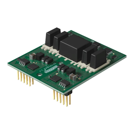
When handling the driver, do not pick up the driver at the transformers. The driver MUST be handled at the PCB sides. Figure 7: SKYPER ® 42 LJ R | Handling instruction © by SEMIKRON / 2019-07-23 / Technical Explanation / SKYPER ® 42 LJ R Page 10/35 PROMGT.1026/ Rev.7/ Template Technical Explanation... -
Page 11: Interface Description
TOP_IN Switching signal input (TOP) 15V logic; 33kΩ/0.01nF (pull-down) LOW = TOP switch off HIGH = TOP switch on © by SEMIKRON / 2019-07-23 / Technical Explanation / SKYPER ® 42 LJ R Page 11/35 PROMGT.1026/ Rev.7/ Template Technical Explanation... -
Page 12: Pin Assignment Of Pin Header X100 | Secondary Side | Top
External blocking diode needed X200:03 PWR_VS_P_BOT Power supply output, Equal to V G(on) positive voltage (external buffer capacitors can be connected) © by SEMIKRON / 2019-07-23 / Technical Explanation / SKYPER ® 42 LJ R Page 12/35 PROMGT.1026/ Rev.7/ Template Technical Explanation... -
Page 13: Power Supply | Primary Side
42 LJ R | Primary side | Power supply ® SKYPER 42 LJ R PWR_VS X10:09 PWR_VS X10:10 PWR_VS PWR_GND X10:01 PWR_GND © by SEMIKRON / 2019-07-23 / Technical Explanation / SKYPER ® 42 LJ R Page 13/35 PROMGT.1026/ Rev.7/ Template Technical Explanation... -
Page 14: Gate Drive Signals | Primary Side
The recommended TOP_IN BOT_IN value of the pull-down resistors is approximately 10kΩ. Parameter Threshold high Threshold low © by SEMIKRON / 2019-07-23 / Technical Explanation / SKYPER ® 42 LJ R Page 14/35 PROMGT.1026/ Rev.7/ Template Technical Explanation... -
Page 15: Filter Selection, Jitter And Propagation Delay Time | Primary Side
42 LJ R | Primary side | Error output ® SKYPER 42 LJ R PWR_VS X10:09 PWR_VS nERR_OUT X10:03 nERR_OUT PWR_GND X10:01 PWR_GND © by SEMIKRON / 2019-07-23 / Technical Explanation / SKYPER ® 42 LJ R Page 15/35 PROMGT.1026/ Rev.7/ Template Technical Explanation... -
Page 16: Error Input | Primary Side
42 LJ R | 2 X10:04 nERR_IN X10:03 nERR_OUT X10:05 CFG_ERR PWR_GND X10:01 PWR_GND Parameter Threshold high 11 V Threshold low 7.5 V © by SEMIKRON / 2019-07-23 / Technical Explanation / SKYPER ® 42 LJ R Page 16/35 PROMGT.1026/ Rev.7/ Template Technical Explanation... -
Page 17: Error Mode Selection | Primary Side
PWR_VS_N which has to be taken into account, in case the NTC thermistor is monitored by an external application circuit as well. © by SEMIKRON / 2019-07-23 / Technical Explanation / SKYPER ® 42 LJ R Page 17/35 PROMGT.1026/ Rev.7/ Template Technical Explanation... - Page 18 CFG(temp) the desired trip level. Parameter Threshold high 13 V Threshold low © by SEMIKRON / 2019-07-23 / Technical Explanation / SKYPER ® 42 LJ R Page 18/35 PROMGT.1026/ Rev.7/ Template Technical Explanation...
-
Page 19: 4.10 Gate Resistors | Secondary Side
G(softoff)_TOP PWR_GND_TOP X100:08 Please note that some of SEMIKRON’s driver cores using an ASIC internal N-channel MOSFET for Soft Off. To protect this MOSFET against back swings when turning-off the TOP_ON/BOT_ON channel it is recommended to place the R resistor in series to the R resistor. -
Page 20: 4.11 External Boost Capacitors | Secondary Side
Please note, when assembling boost capacitors at the secondary side, also boost capacitors has to be assembled at the primary side, as shown in Figure 9. �� = �� = �� ������ ������(��) ������(��) © by SEMIKRON / 2019-07-23 / Technical Explanation / SKYPER ® 42 LJ R Page 20/35 PROMGT.1026/ Rev.7/ Template Technical Explanation... -
Page 21: Protection Features
>9µs no input signals at TOP_IN/BOT_IN (Customer confirms error) After completing the reset sequence the driver returns ‘ready for operation’ by setting the nERR_OUT output to high-level. © by SEMIKRON / 2019-07-23 / Technical Explanation / SKYPER ® 42 LJ R Page 21/35 PROMGT.1026/ Rev.7/ Template Technical Explanation... - Page 22 1) The signal characteristics of BOT_ON/OFF and TOP_ON/OFF are valid if the outputs X100:06 and X100:07 respectively the outputs X200:06 and X200:07 are connected to each other through the gate resistors. © by SEMIKRON / 2019-07-23 / Technical Explanation / SKYPER ® 42 LJ R Page 22/35 PROMGT.1026/ Rev.7/ Template Technical Explanation...
-
Page 23: Dead Time And Interlock
No dead time Important Note When the interlock function is disabled a bridge shoot through has to be prevented by the customer’s control unit. © by SEMIKRON / 2019-07-23 / Technical Explanation / SKYPER ® 42 LJ R Page 23/35... -
Page 24: Short Pulse Suppression (Sps)
Secondary side non-error threshold, positive gate voltage 13.3V Secondary side shutdown threshold, negative gate voltage -4.1V Secondary side non-error threshold, negative gate voltage -5.8V © by SEMIKRON / 2019-07-23 / Technical Explanation / SKYPER ® 42 LJ R Page 24/35 PROMGT.1026/ Rev.7/ Template Technical Explanation... -
Page 25: Dynamic Short Circuit Protection By
It is not designed for any kind of application over current detection. SEMIKRON recommends to set the DSCP trip level to value of 7V to 9V (voltage at the CFG_VCE pin) to prevent unwanted accidently triggered desaturation events due to a too small gap between the saturation voltage of the IGBT and the trigger level of the DSCP feature. -
Page 26: Dscp | Functional Description
42 LJ R | Dynamic short circuit protection CE(ref) CE(stat) CE(IN) CE(sat) CE(ref) bl(VCE) CE(stat) CE(IN) CE(IN) CE(stat) CE(sat) CE(ref) CE(sat) bl(VCE) bl(VCE) © by SEMIKRON / 2019-07-23 / Technical Explanation / SKYPER ® 42 LJ R Page 26/35 PROMGT.1026/ Rev.7/ Template Technical Explanation... -
Page 27: Dscp | Calculation Hints
Figure 20: SKYPER ® 42 LJ R | Active clamping G(on) Zener DC-Link clamping active G(off) CEsat © by SEMIKRON / 2019-07-23 / Technical Explanation / SKYPER ® 42 LJ R Page 27/35 PROMGT.1026/ Rev.7/ Template Technical Explanation... -
Page 28: Soft Off
Target is to stay within the short circuit proofed time of the IGBT but at the same time reduce the overvoltage below the maximum collector-emitter voltage of the IGBT. © by SEMIKRON / 2019-07-23 / Technical Explanation / SKYPER ®... -
Page 29: Safe Short Circuit Turn-Off In Multilevel Topology
Thoroughly reading this document is highly recommended before starting tests of multilevel topologies. Electrical characteristic Figure 22: SKYPER ® 42 LJ R | Maximum switching frequency © by SEMIKRON / 2019-07-23 / Technical Explanation / SKYPER ® 42 LJ R Page 29/35 PROMGT.1026/ Rev.7/ Template Technical Explanation... -
Page 30: Product Qualification
± y, ± z The test conditions are not the maximum applicable conditions for the products. The characteristics of the products are indicated in the data sheet © by SEMIKRON / 2019-07-23 / Technical Explanation / SKYPER ® 42 LJ R Page 30/35 PROMGT.1026/ Rev.7/ Template Technical Explanation... -
Page 31: Environmental Conditions
1000 Shocks (6 axis; +-x, +-y, +-z, 1000 shocks per axis), 30g, 18ms Connection between driver and PCB has to be reinforced by support post © by SEMIKRON / 2019-07-23 / Technical Explanation / SKYPER ® 42 LJ R Page 31/35... -
Page 32: Marking
Figure 23: SKYPER ® 42 LJ R | Label Every driver core is marked with a data matrix label. The marking contains the following items. © by SEMIKRON / 2019-07-23 / Technical Explanation / SKYPER ® 42 LJ R Page 32/35... -
Page 33: 10. Change History
2017-03-07 Update error diagram, Vce values, clamping 2017-09-13 Update creepage/clearance 2017-10-17 Update handling instruction 2019-07-23 Update to new design © by SEMIKRON / 2019-07-23 / Technical Explanation / SKYPER ® 42 LJ R Page 33/35 PROMGT.1026/ Rev.7/ Template Technical Explanation... - Page 34 [3] P. Bhosale, M. Hermwille, AN-7002 “Connection of Gate Drivers to IGBT and Controller” [4] M. Hermwille, AN-7003 “Gate Resistor – Principles and Applications” [5] J. Lamp, AN 19-001 “Gate Driver Configuration and Short Circuit Protection for 3-Level Topologies” © by SEMIKRON / 2019-07-23 / Technical Explanation / SKYPER ® 42 LJ R Page 34/35 PROMGT.1026/ Rev.7/ Template Technical Explanation...
- Page 35 SEMIKRON does not assume any liability arising out of the applications or use of any product; neither does it convey any license under its patent rights, copyrights, trade secrets or other intellectual property rights, nor the rights of others.
Need help?
Do you have a question about the SKYPER 42 LJ R and is the answer not in the manual?
Questions and answers