Table of Contents
Advertisement
Quick Links
Technical Explanation
®
SKiiP
4
Please note:
Unless otherwise specified, all values in this technical explanation are typical values. Typical values are
average values derived from large quantities of tested SKiiPs and are provided for information purposes
only, thus, they're not a binding specification. These values can and do vary under different application
conditions. All operating parameters must be validated by the user's technical experts for each
application.
This document is valid for the following SKiiP
20601123
SKiiP 1814 GB12E4-3DUL
20601224
SKiiP 1814 GB17E4-3DUL
20601125
SKiiP 2414 GB12E4-4DUL
20601226
SKiiP 2414 GB17E4-4DUL
20601127
SKiiP 3614 GB12E4-6DUL
20601228
SKiiP 3614 GB17E4-6DUL
20601133
SKiiP 1814 GB12E4-3DUW
20601234
SKiiP 1814 GB17E4-3DUW
20601135
SKiiP 2414 GB12E4-4DUW
20601236
SKiiP 2414 GB17E4-4DUW
20601137
SKiiP 3614 GB12E4-6DUW
20601238
SKiiP 3614 GB17E4-6DUW
20601139
SKiiP 1814 GB12E4-3DUL
20601240
SKiiP 1814 GB17E4-3DUL
20601141
SKiiP 2414 GB12E4-4DUL
20601242
SKiiP 2414 GB17E4-4DUL
20601143
SKiiP 3614 GB12E4-6DUL
20601244
SKiiP 3614 GB17E4-6DUL
20601159
SKiiP 3614 GB12E4-6DULR
20601174
SKiiP 1814 GB12E4-3DUSL
20601175
SKiiP 2414 GB12E4-4DUSL
20601176
SKiiP 3614 GB12E4-6DUSL
20601277
SKiiP 3614 GB17E4-6DULR
This technical explanation document is valid as well for customized SKiiP
and 20602xxx (SKiiPxx-Dxxxx) excepting restrictions or features which are subject of a customized
specification. The document remains effective until replaced by a subsequent revision of this document.
© by SEMIKRON / 2017-09-07 / Technical Explanation / SKiiP
PROMGT.1023/ Rev.4/ Template Technical Explanation
Revision:
Issue date:
Prepared by:
Approved by:
Keyword: SKiiP4 technical explanation, Application note
®
4 part numbers:
20602023
SKiiP 1814 GB12E4-3DUL
20602024
SKiiP 1814 GB17E4-3DUL
20602025
SKiiP 2414 GB12E4-4DUL
20602026
SKiiP 2414 GB17E4-4DUL
20602027
SKiiP 3614 GB12E4-6DUL
20602028
SKiiP 3614 GB17E4-6DUL
20602033
SKiiP 1814 GB12E4-3DUW
20602034
SKiiP 1814 GB17E4-3DUW
20602035
SKiiP 2414 GB12E4-4DUW
20602036
SKiiP 2414 GB17E4-4DUW
20602037
SKiiP 3614 GB12E4-6DUW
20602038
SKiiP 3614 GB17E4-6DUW
20602039
SKiiP 1814 GB12E4-3DUL
20602040
SKiiP 1814 GB17E4-3DUL
20602041
SKiiP 2414 GB12E4-4DUL
20602042
SKiiP 2414 GB17E4-4DUL
20602043
SKiiP 3614 GB12E4-6DUL
20602044
SKiiP 3614 GB17E4-6DUL
20602059
SKiiP 3614 GB12E4-6DULR
20602074
SKiiP 1814 GB12E4-3DUSL
20602075
SKiiP 2414 GB12E4-4DUSL
20602076
SKiiP 3614 GB12E4-6DUSL
20602077
SKiiP 3614 GB17E4-6DULR
®
4
11
2017-09-07
Marco Honsberg
Joachim Lamp
®
4 with part numbers 20601xxx
Page 1/73
Advertisement
Chapters
Table of Contents

Related Manuals for SEMIKRON SKiiP 4


Summary of Contents for SEMIKRON SKiiP 4
- Page 1 20602xxx (SKiiPxx-Dxxxx) excepting restrictions or features which are subject of a customized specification. The document remains effective until replaced by a subsequent revision of this document. ® © by SEMIKRON / 2017-09-07 / Technical Explanation / SKiiP Page 1/73 PROMGT.1023/ Rev.4/ Template Technical Explanation...
-
Page 2: Table Of Contents
7.9 Recommended temperature rating ..................60 7.10 Switching operation and current sharing between paralleled half bridge modules ......63 ® 7.11 Paralleling of SKiiP 4 ......................63 ® © by SEMIKRON / 2017-09-07 / Technical Explanation / SKiiP Page 2/73... - Page 3 8.1.3 Warranty Label ......................67 8.1.4 Data Matrix Code ......................67 8.1.5 Provisions and handling after use ..................68 9. Abbreviations ........................... 71 10. Symbols ..........................72 ® © by SEMIKRON / 2017-09-07 / Technical Explanation / SKiiP Page 3/73...
-
Page 4: Related Documents
Technical Explanation SKiiP 4 F-Option • Technical Explanation SKiFace Adapter Board All these documents can be found on the SEMIKRON internet page (www.semikron.com) or requested at SEMIKRON ® © by SEMIKRON / 2017-09-07 / Technical Explanation / SKiiP Page 4/73... -
Page 5: Introduction
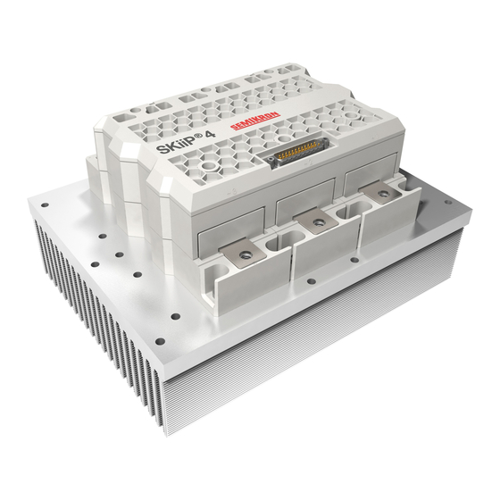
® The 4 generation SKiiP “SKiiP 4” is an Intelligent Power Module (IPM) with highest power density and reliability. SEMIKRON’s SKiiP stands for “SEMIKRON intelligent integrated Power” indicating that three components are integrated into one IPM: • heat sink •... -
Page 6: Heat Sink
Figure 2.3: Half bridge “exploded assembly view” Heat sink SEMIKRON offers highly efficient water cooled heat sinks and air cooled aluminum heat sinks. Detailed technical parameter are given in the datasheet of the corresponding SKiiP. Customer specific heat sinks can be designed, simulated, measured and assembled on request as well. -
Page 7: Gate Drive Unit
Figure 2.4: Main terminals construction principle In the SKiiP 4 in contrast to previous generations of SKiiPs the bare chips are sintered and not soldered. The sophisticated sintering process is based on a pulverized silver which creates a robust material connection when suitable pressure and temperature is applied during the formation process. -
Page 8: Topologies And Selection Guide
Topologies and selection guide Type Designation Code ® © by SEMIKRON / 2017-09-07 / Technical Explanation / SKiiP Page 8/73... -
Page 9: Overview Of The Available Types And Current Ratings
SKiiP SKiiP SKiiP SKiiP SKiiP SKiiP 1814GB12E4- 1814GB17E4 2414GB12E4- 2414GB17E4- 3614GB12E4- 3614GB17E4- 3DUL -3DUL 4DUL 4DUL 6DUL 6DUL = 1800A = 2400A = 3600A Cnom Cnom Cnom ® © by SEMIKRON / 2017-09-07 / Technical Explanation / SKiiP Page 9/73... -
Page 10: Standards And Qualification Tests
Frequency: 150 kHz - 80 MHz Voltage: 20V EMF Modulation: 80 % AM, 1kHz Magnet field (61000-4-8) Far field, homogeneous 170A/m Electrostatic discharge (ESD) Contact discharge EN 61000-4-2 Air discharge ® © by SEMIKRON / 2017-09-07 / Technical Explanation / SKiiP Page 10/73... -
Page 11: Isolation Coordination
According to HD625 S1 and IEC60664-1 the maximum altitude can be calculated based on the factors between required and designed clearance distances. ® © by SEMIKRON / 2017-09-07 / Technical Explanation / SKiiP Page 11/73... -
Page 12: Table 4-4: Altitude Correction Factors (Iec 60664-1)
II an altitude of theoretically 9000 m for SKiiP 4 is possible. This is the case when an additional basic isolation is implemented between the SKiiP 4 driver interface and controller board. This can be realized by the following means: •... -
Page 13: Figure 4.3: Implementation Of Additional Basic Isolation Between Skiip
® Figure 4.3: Implementation of additional basic isolation between SKiiP 4 driver interface and controller board Finally, the installation altitude of the SKiiP 4 depends on: • Grid configuration (star grounded grid, delta grounded grid) • The voltage level of the line to earth voltage (rated isolation voltage) •... -
Page 14: Figure 7.5: Skiip
Factor 1,75 1,75 Altitude 2000m 6250m 2000m 6250m Maximum Altitude with safety 2000m 4840m 2000m 6250m isolation Maximum Altitude without safety 2000m 4840m 4840m 9000m isolation ® © by SEMIKRON / 2017-09-07 / Technical Explanation / SKiiP Page 14/73... -
Page 15: Gate Driver Board
Gate driver interface SKiFace marked as red block in Figure 5.1 (refer to Chapter 5.2) • Gate driver board, marked as green block in Figure 5.1 (refer to Chapter 5.3) Figure 5.1: Gate Driver Board block diagram ® © by SEMIKRON / 2017-09-07 / Technical Explanation / SKiiP Page 15/73... -
Page 16: Gate Driver Interface "Skiface
4 to a control circuit the following recommendations shall be observed for a proper cable selection: • Cable length should be kept shorter than 3m • Utilization of shielded cables is recommended • Longer cables must be shielded ® © by SEMIKRON / 2017-09-07 / Technical Explanation / SKiiP Page 16/73... -
Page 17: Pin Description
A verification of mechanical stability and EMC behaviour under customer’s application conditions is necessary. As the SKiFace interface is a standardized, it is also used in other SEMIKRON products. Due to that not all ® signals are used for SKiiP... - Page 18 CMN_HB_RSRVD HB_I_GND Ground for HB_I CAN interface INPUT/ Input impedance = very high; CAN_L OUTPUT LOW Specification according to ISO 11898. CAN_L Internally connected to pin 24 ® © by SEMIKRON / 2017-09-07 / Technical Explanation / SKiiP Page 18/73...
-
Page 19: Figure 5.4: Overview Schematics Skiface Interface
HB_I_GND = Analogue ground Digital output Digital input HB_TOP = Switching signal TOP Digital output Digital input HB_BOT = Switching signal BOT CAN_H CAN_H CAN_H CAN_H CAN_L CAN_L CAN_L CAN_L ® © by SEMIKRON / 2017-09-07 / Technical Explanation / SKiiP Page 19/73... -
Page 20: External Power Supply
Please note: Do not apply switching signals during power up. The external power supply requires the capability to feed a minimum inrush current into the SKiiP 4 at start-up of the system without entering a fault state itself. Typically power supplies with fold-back characteristic or hiccup-mode can create problems if insufficient over current margin is available. -
Page 21: Switching Signal Inputs
: Minimum threshold that guarantees that input voltage level is recognized to switch on the IGBT. : Maximum threshold that guarantees that input voltage level is recognized to switch off the IGBT. All threshold values are related to the supply voltage V ® © by SEMIKRON / 2017-09-07 / Technical Explanation / SKiiP Page 21/73... -
Page 22: Analogue Output Signals
(refer to Figure 5.13). ® © by SEMIKRON / 2017-09-07 / Technical Explanation / SKiiP Page 22/73... -
Page 23: Figure 5.8: Application Example - Symmetric Wired Differential Amplifier. Terminal Description Hb_I And
• AGND should be connected to the ground of the analogue signal processing at the user controller board. ® © by SEMIKRON / 2017-09-07 / Technical Explanation / SKiiP Page 23/73... -
Page 24: Halt Logic Signal
This parallel connection of HALT signals provides a fast disabling of IGBT switching in case of an error or power up. Hence, the operation of such paralleled SKiiP 4can only start when all SKiiP 4 are ready to operate. The HALT signals of all SKiiPs in the application can be connected to the controller separately, too, as shown in Figure 5.9. -
Page 25: Figure 5.9: Application Example Of The Halt Signal Processing For Separated Skiip
4 systems Please note: If the HALT signal is not used it must be connected to the Vs pin according to Figure 5.16 (not used digital signals). ® © by SEMIKRON / 2017-09-07 / Technical Explanation / SKiiP Page 25/73... -
Page 26: Cmn_Gpio1 Signal
® CMN_GPIO1 output of several SKiiP Figure 5.10: Application example of the CMN_GPIO1 (inverted HALT signal) as error output signal ® © by SEMIKRON / 2017-09-07 / Technical Explanation / SKiiP Page 26/73... -
Page 27: Canbus Interface
5.2.8 CANbus interface The CANbus interface employs comprehensive interaction with the SKiiP 4, e.g. it provides the possibility to read out the type of error occurred and when it occurred. In addition to this, the CAN-interface is used to ®... - Page 28 For a detailed description of the SKiiP4 CAN interface please refer to the following documents • Diagnostic Interface SKiiP4 – CANopen User Manual • Diagnostic Interface SKiiP4 – CANopen Object Dictionary ® © by SEMIKRON / 2017-09-07 / Technical Explanation / SKiiP Page 28/73...
-
Page 29: Ground Connection
PCB to chassis) and located close to the D-Sub connector. Furthermore each signal output and input should have a capacitor to chassis. These measures are for bypassing burst signals. ® © by SEMIKRON / 2017-09-07 / Technical Explanation / SKiiP Page 29/73... -
Page 30: 5.2.11 Reserved Or Not Used Signals
For the CAN interface it is recommended to connect the CAN open signals by 121 Ohm resistor, in case the CAN interface will not be used. Unused analogue signals should be connected to GND by a 10kOhm resistor. ® © by SEMIKRON / 2017-09-07 / Technical Explanation / SKiiP Page 30/73... -
Page 31: Gate Driver Board
The driver board processes a Power-On-Reset after turning on the supply voltage. During t the HALT signal is set to LOW. Without any error being present, the HALT signal will be released (recessive HIGH- State) after the Power-On-Reset is completed. ® © by SEMIKRON / 2017-09-07 / Technical Explanation / SKiiP Page 31/73... -
Page 32: Interlock Dead Time Generation
In this way the IGBTs are protected against noise which can occur due to burst on the signal lines. If a pulse is shorter than t , it will be suppressed, the other channel will remain on. No error signal will be issued. ® © by SEMIKRON / 2017-09-07 / Technical Explanation / SKiiP Page 32/73... -
Page 33: Intellioff
The suitable gate turn-off speed will be chosen as a function of the actual measured AC current value. As shown in Figure 5.19, there are two different turn-off speed scenarios: Figure 5.19 : Turn-off speed scenarios ® © by SEMIKRON / 2017-09-07 / Technical Explanation / SKiiP Page 33/73... -
Page 34: Table 5-4: Intellioff Functionality
The GPIO2 must be assigned to this functionality before by a command through the CAN interface. Then ® the ports of all parallel operating SKiiP 4 modules have to be connected. ® © by SEMIKRON / 2017-09-07 / Technical Explanation / SKiiP Page 34/73... -
Page 35: Error Management
4 data sheet, page 2), if the supply voltage exceeds the reset threshold level after the failure reason has disappeared and if the switching input signals HB_TOP and HB_BOT are set to LOW. ® © by SEMIKRON / 2017-09-07 / Technical Explanation / SKiiP Page 35/73... -
Page 36: Figure 5.20: Switching Frequency Range
IGBT will be turned-on. The timing diagram of the error processing in case the overlapping duration is shorter than 3µs, is shown in the Figure 5.21. Figure 5.21: Timing diagram for the TOP/BOT overlapping error processing (t<3µs) ® © by SEMIKRON / 2017-09-07 / Technical Explanation / SKiiP Page 36/73... -
Page 37: Figure 5.22: Timing Diagram For The Hb_Top/Hb_Bot Overlapping Error Processing (T>3Μs)
The application shall be selected to ensure that the peak load current stays safely below the over current protection level. For further details please refer to the corresponding datasheet of the SKiiP 4. 5.3.7.6... -
Page 38: Analogue Signals / Sensor Functionality
±3% TRIPSC Small signal bandwidth, f0 50 kHz Iana ® Figure 5.26: Characteristics between current and the voltage at HB_I, SKiiP 4 3-fold ® © by SEMIKRON / 2017-09-07 / Technical Explanation / SKiiP Page 38/73... - Page 39 ® © by SEMIKRON / 2017-09-07 / Technical Explanation / SKiiP Page 39/73...
- Page 40 Figure 5.27: Characteristic between current and the voltage at HB_I, SKiiP 4 4-fold ® Figure 5.28: Characteristic between current and the voltage at HB_I, SKiiP 4 6-fold ® © by SEMIKRON / 2017-09-07 / Technical Explanation / SKiiP Page 40/73...
-
Page 41: Figure 5.29: Bode Diagram Of The Ac-Current Measurement At The Skiip4 Interface
Figure 5.30 illustrates the compensation principle with the current ® sensor employed in the SKiiP ® Figure 5.30: Compensation principle of SKiiP 4 current sensor ® © by SEMIKRON / 2017-09-07 / Technical Explanation / SKiiP Page 41/73... -
Page 42: Figure 5.31: Characteristic Between Dcb-Sensor Temperature And The Voltage At Cmn_Temp
90°C again and if the switching input signals HB_TOP and HB_BOT are set to LOW the HALT signal will be released (recessive HIGH state). ® © by SEMIKRON / 2017-09-07 / Technical Explanation / SKiiP Page 42/73... -
Page 43: Table 5-10
The characteristic between the DC-Link voltage and the signal on CMN_DCL for 1200V and 1700V SKiiP systems can be found in the Figure 5.32 and Figure 5.33 corresponding. ® © by SEMIKRON / 2017-09-07 / Technical Explanation / SKiiP Page 43/73... -
Page 44: Figure 5.32: Dc Link Voltage Sensor Output 1200V System
4 for 1500V photovoltaic applications do not protect against an DC-link overvoltage. The user must take care of keeping the DC-link voltage within suitable limits in the application. ® © by SEMIKRON / 2017-09-07 / Technical Explanation / SKiiP Page 44/73... -
Page 45: Figure 5.34: Bode Diagram Of The Dc-Link Voltage Measurement At The Skiip4 Interface
Figure 5.34: Bode diagram of the DC-link voltage measurement at the SKiiP4 interface ® © by SEMIKRON / 2017-09-07 / Technical Explanation / SKiiP Page 45/73... -
Page 46: Power Terminals
The maximum forces that must not be exceeded are given in Table 6—1 Table 6—1: Maximum allowable forces to terminals Force Maximum allowed force ® © by SEMIKRON / 2017-09-07 / Technical Explanation / SKiiP Page 46/73... -
Page 47: Figure 6.1: Maximum Forces At The Main Terminals
The plate should be fixed by fixing poles. These poles shall be mounted directly on to the heat sink or a fixed frame construction and placed close to the SKiiP device. The design has to be as depicted in Figure 6.2 ® © by SEMIKRON / 2017-09-07 / Technical Explanation / SKiiP Page 47/73... -
Page 48: Figure 6.2: Ac Connection
Figure 6.2: AC connection Please note: All screws of the AC terminals must be tightened uniformly (not one screw completely fixed before the others) to avoid the warping. ® © by SEMIKRON / 2017-09-07 / Technical Explanation / SKiiP Page 48/73... -
Page 49: Application Hints
Please note: The curves for Safe Operating Area (SOA) of 1500V photovoltaic SKiiP 4 Systems are shown in the relevant data sheet and differ from this SOA. ® © by SEMIKRON / 2017-09-07 / Technical Explanation / SKiiP Page 49/73... -
Page 50: Maximum Blocking Voltage And Snubber Capacitors
Power losses of the chip losses In general, the thermal resistance between two points 1 and 2 is defined according to following equation: − ∆ − losses losses ® © by SEMIKRON / 2017-09-07 / Technical Explanation / SKiiP Page 50/73... -
Page 51: Cooling And Coolant Circuit
Please note: The values for transient thermal impedance given in the data sheets (Z ) are only th(j-r) valid together with the SEMIKRON standard heat sinks and under conditions given in the data sheets. The usage of these values for other heat sinks/conditions might cause deviations in calculation of thermal resistance! Cooling and coolant circuit 7.5.1... - Page 52 The user has to ensure that the used coolant is compatible with the cooling circuit materials to avoid e.g. corrosion or freezing at low temperatures. SEMIKRON proposes the usage of a mixture of water and glycol with corrosion inhibitor. The percentage of glycol in the cooling medium shall be at least 10%. All thermal ®...
-
Page 53: Water Connection Description Of Water-Cooled Skiip ® 4
Fitting of shape G according to ISO 1179-3 • with G ½ thread, tolerance class A (DIN EN ISO 228), G is the type of the sealing ® © by SEMIKRON / 2017-09-07 / Technical Explanation / SKiiP Page 53/73... -
Page 54: Figure 7.7: Description Of Fitting Iso 1179-3 - G 1/2 A - G
Please note: The given specifications for gaskets of the pipe fittings are recommended values and have to be validated by customer depending on production equipment and application. ® © by SEMIKRON / 2017-09-07 / Technical Explanation / SKiiP Page 54/73... -
Page 55: Isolation Voltage Test (Ivt)
IVT a test with DC voltage is recommended because in case of AC IVT the high leakage currents hardly help in the identification of the isolation problem root cause. ® © by SEMIKRON / 2017-09-07 / Technical Explanation / SKiiP Page 55/73... -
Page 56: Frt (Fault Ride Through) - Function
Parts of this requirements are known as Fault Ride Through (FRT) or Low Voltage Ride Through (LVRT). ® © by SEMIKRON / 2017-09-07 / Technical Explanation / SKiiP Page 56/73... -
Page 57: Figure 7.9: Graphic Schematic Of The Wind Mill
In this case CMN_GPIO1 will not be the inverted CMN_HALT signal anymore. An overcurrent trip will never set CMN_HALT to LOW and it is never stored in the SKiiP error memory. ® © by SEMIKRON / 2017-09-07 / Technical Explanation / SKiiP Page 57/73... -
Page 58: Figure 7.11: Graphic Presentation Of Skiip
SKiiP diodes will not be overloaded. The FRT-Function can be activated through the CAN-Bus interface. Please refer to the CAN user’s manual documentation for further details. ® © by SEMIKRON / 2017-09-07 / Technical Explanation / SKiiP Page 58/73... -
Page 59: Solar Function
® Figure 7.13: SOA for SKiiP 4 Solar ® The operation modes for SKiiP 4 solar are listed in the Table 7—2. ® © by SEMIKRON / 2017-09-07 / Technical Explanation / SKiiP Page 59/73... -
Page 60: Recommended Temperature Rating
(failures known as early failures), then dropping to a low and more or less constant value (the random failures) before it rises again as wear-out begins to set in and end-of-life failures set a limit to the useful life of a component. ® © by SEMIKRON / 2017-09-07 / Technical Explanation / SKiiP Page 60/73... -
Page 61: Figure 7.14: Probability Of A Failure During Operation Time
Dedicated calculations shall be carried out by the SEMIKRON simulation tool SEMISEL which is available on the SEMIKRON homepage www.semikron.com. Load cycles and cooling conditions can be adapted to meet the application conditions. The measurement ®... -
Page 62: Figure 7.16: Position Of The Driver Temperature Sensor Skiip4
If necessary the trip level of the temperature sensor can be adjusted to a lower level by the CAN-bus interface. Figure 7.16: Position of the driver temperature sensor SKiiP4 ® © by SEMIKRON / 2017-09-07 / Technical Explanation / SKiiP Page 62/73... -
Page 63: 7.10 Switching Operation And Current Sharing Between Paralleled Half Bridge Modules
This can be done e.g. by Rogowski current sensors which are located around the DC+ and DC- terminals. ® 7.11 Paralleling of SKiiP The parallel operation of SKiiP 4’s requires the following considerations and features: ® • Common error management for all paralleled SKiiP 4 can be realized using the HALT signal •... -
Page 64: Figure 7.17: An Example Of Skiip
This is shown in Figure 7.18. The value t is given in the SKiiP 4 data sheet on page 2. jitter ® Figure 7.18: Effects of paralleling SKiiP ® © by SEMIKRON / 2017-09-07 / Technical Explanation / SKiiP Page 64/73... -
Page 65: 7.12 Prevention Of Condensation
This can be done by air heater in air cooled systems or by pre-heated water in water cooled systems before connecting the operation voltage to the SKiiP. ® © by SEMIKRON / 2017-09-07 / Technical Explanation / SKiiP Page 65/73... -
Page 66: Logistics
In case of technical inquiries please always refer to the SKiiP Item number written on this label. ® Figure 8.1: System Label of SKiiP ® © by SEMIKRON / 2017-09-07 / Technical Explanation / SKiiP Page 66/73... -
Page 67: Half Bridge Laser Label
10 digits free for customer information 3 digits continuously module number 2 digits additionally order number 10 digits production order number 2 digits 8 digits SKiiP item number ® © by SEMIKRON / 2017-09-07 / Technical Explanation / SKiiP Page 67/73... -
Page 68: Provisions And Handling After Use
8.1.5 Provisions and handling after use Components which are obsolete or defective must be disposed according to local regulations ® © by SEMIKRON / 2017-09-07 / Technical Explanation / SKiiP Page 68/73... - Page 69 4 behaviour with FRT-function activated in case of overcurrent58 Figure 7.12: Graphic presentation of the driver processing in FRT-case ..........58 ® Figure 7.13: SOA for SKiiP 4 Solar ....................59 ® © by SEMIKRON / 2017-09-07 / Technical Explanation / SKiiP Page 69/73...
- Page 70 Table 7—1: Snubber capacitors for SKiiP 4 ..................50 ® Table 7—2: Operation modes SKiiP 4 solar ..................60 Table 7—3: Default values for the T ..................62 Driver Trip ® © by SEMIKRON / 2017-09-07 / Technical Explanation / SKiiP Page 70/73...
-
Page 71: Abbreviations
Positive Temperature Coefficent Relative Humidity RoHS Restriction of Hazardous Substances Short Circuit Protection SKiiP Semikron intelligent integrated Power Short Pulse Suppression Under Voltage Protection Safe Operating Area ® © by SEMIKRON / 2017-09-07 / Technical Explanation / SKiiP Page 71/73... -
Page 72: 10. Symbols
HALT Over temperature trip level DriverTrip Bandwidth of DC-voltage measurement @ VDctrip Uana Bandwidth of current measurement @ ITRIPSC Iana Bandwidth of temperature measurement @ Ttrip Tana ® © by SEMIKRON / 2017-09-07 / Technical Explanation / SKiiP Page 72/73... - Page 73 A detailed explanation of the terms and symbols can be found in the “Application Manual Power Semiconductors” [2] References [1] www.SEMIKRON.com [2] A. Wintrich, U. Nicolai, W. Tursky, T. Reimann, “Application Manual Power Semiconductors”, ISLE Verlag 2011, ISBN 978-3-938843-666 ® © by SEMIKRON / 2017-09-07 / Technical Explanation / SKiiP Page 73/73...
Need help?
Do you have a question about the SKiiP 4 and is the answer not in the manual?
Questions and answers