Table of Contents
Advertisement
Quick Links
IMPORTANT INFORMATION ABOUT LEAD FREE, (PbF), SOLDERING
If lead free solder was used in the manufacture of this product the printed circuit boards will be marked PbF.
Standard leaded, (Pb), solder can be used as usual on boards without the PbF mark.
When this mark does appear, please read and follow the special instructions described in this manual on the use of PbF and how
it might be permissible to use Pb solder during service and repair work.
Advanced Hybrid System
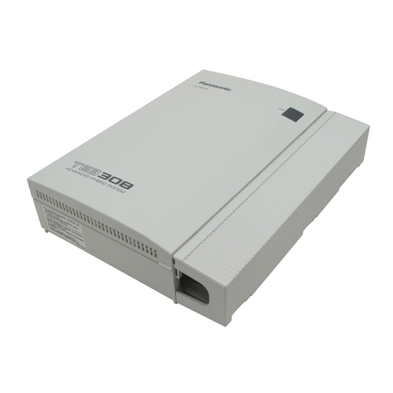
KX-TEA308CE
KX-TE82460X
KX-TE82492X
KX-TE82493X
KX-A227X
(for Europe)
© 2005 Panasonic Communications Co., Ltd. All
rights
reserved.
distribution is a violation of law.
ORDER NO. KMS0506086CE
Unauthorized
copying
and
Advertisement
Table of Contents

Related Manuals for Panasonic KX-TEA308CE


Summary of Contents for Panasonic KX-TEA308CE
- Page 1 When this mark does appear, please read and follow the special instructions described in this manual on the use of PbF and how it might be permissible to use Pb solder during service and repair work. © 2005 Panasonic Communications Co., Ltd. All rights reserved.
-
Page 2: Table Of Contents
9.3. KX-TEA308CE MAIN BLOCK DIAGRAM 17 CABINET AND ELECTRICAL PARTS LOCATION 9.4. KX-TEA308CE CO BLOCK DIAGRAM 18 ACCESSORIES AND PACKING MATERIALS 9.5. KX-TEA308CE POWER SUPPLY UNIT BLOCK 19 REPLACEMENT PARTS LIST (KX-TEA308CE) DIAGRAM 19.1. CABINET AND ELECTRICAL PARTS 10 EXPLANATION OF BLOCK DIAGRAM 19.2. - Page 3 KX-TEA308CE 23.2. LOCATION OF OPTIONAL CARDS 24.8. ACCESSORIES AND PACKING MATERIALS 23.3. DOORPHONE/DOOROPENER CARD BLOCK DIAGRAM 24.9. REPLACEMENT PARTS LIST (KX-TE82492X) 24.10. FOR THE SCHEMATIC DIAGRAM 23.4. EXPLANATION OF BLOCK DIAGRAM/CIRCUIT 24.11. SCHEMATIC DIAGRAM (KX-TE82492X) OPERATIONS 24.12. PRINTED CIRCUIT BOARD (KX-TE82492X) 23.5.
-
Page 4: About Lead Free Solder (Pbf: Pb Free)
KX-TEA308CE 1 ABOUT LEAD FREE SOLDER (PbF: Pb free) Note: In the information below, Pb, the symbol for lead in the periodic table of elements, will refer to standard solder or solder that contains lead. We will use PbF solder when discussing the lead free solder used in our manufacturing process which is made from Tin, (Sn), Silver, (Ag), and Copper, (Cu). -
Page 5: How To Recognize That Pb Free Solder Is Used
KX-TEA308CE 1.2. HOW TO RECOGNIZE THAT Pb FREE SOLDER IS USED... - Page 6 KX-TEA308CE...
-
Page 7: For Service Technicians
KX-TEA308CE 2 FOR SERVICE TECHNICIANS ICs and LSIs are vulnerable to static electricity. When repairing, the following precautions will help prevent recurring malfunctions. 1. Cover the plastic parts boxes with aluminum foil. 2. Ground the soldering irons. 3. Use a conductive mat on the worktable. -
Page 8: Caution
KX-TEA308CE 3 CAUTION 3.1. SAFETY PRECAUTIONS 1. Before servicing, unplug the power cord to prevent an electric shock. 2. When replacing parts, use only the manufacturer´s recommended components for safety. 3. Check the condition of the power cord. Replace if wear or damage is evident. -
Page 9: Specifications
KX-TEA308CE 4 SPECIFICATIONS 4.1. GENERAL DESCRIPTION Control Bus Original bus (16-bit, 24 MHz) Switching Space Division CMOS Crosspoint Switch Power Input 100 V AC to 240 V AC, 0.8A to 0.4A, 50 Hz/60Hz External Battery +24 V DC (+12 V DC x 2) -
Page 10: System Overview
KX-TEA308CE 4.3.2. Maximum Cards Terminal Equipment ltem KX-TEA308 2-Port Doorphone Card 3-Port Caller ID Card 2-Channel Voice Message Card Doorphone Door Opener Pager Music on Hold (MOH) DSS Console 4.3.3. System Data ltem Max. Quantity Operator System Speed Dialling One-touch Dialling... -
Page 11: System Connection Diagram
KX-TEA308CE 5.2. SYSTEM CONNECTION DIAGRAM • • • • Connect a display-equipped proprietary telephone (PT) to extension jack 01, as this extension is automatically designated as the manager extension. -
Page 12: Names And Locations
KX-TEA308CE 6 NAMES AND LOCATIONS 7 CONNECTION 7.1. SERIAL INTERFACE CONNECTION... -
Page 13: Disassembly Instructions
KX-TEA308CE 8 DISASSEMBLY INSTRUCTIONS 8.1. DISASSEMBLY INSTRUCTION 1. Pull the slide button (arrow 1) to the right and, holding it, slide the cable cover upwards (arrow 2). 2. Then turn the cable cover slightly to remove it. 3. Remove the three screws (A). - Page 14 KX-TEA308CE 5. Remove the 1 screws (A). 6. Remove the power supply board cover. 7. Pull out the 4 connectors. 8. Remove the 2 screw (B) and 1 screw (A). 9. Remove the power supply board. 10. Remove the 2 screw (B).
-
Page 15: Block Diagram
KX-TEA308CE 9 BLOCK DIAGRAM 9.1. SYSTEM BLOCK DIAGRAM... -
Page 16: Power Block Diagram
KX-TEA308CE 9.2. POWER BLOCK DIAGRAM 9.3. KX-TEA308CE MAIN BLOCK DIAGRAM CN708 EXT1-8 Door Phone CROSS EXT1 DOOR1,2 Door Opener POINT IC606, IC607 CONNECTOR DTMFR(1,2) TAM1-2,TONE CN707 IC601 EXT2 (For EXT) BV Card IC602 CONNECTOR IC603 620,440,350Hz CO1-3 EXT3 CN701 PAGE... -
Page 17: Kx-Tea308Ce Co Block Diagram
KX-TEA308CE 9.4. KX-TEA308CE CO BLOCK DIAGRAM 9.5. KX-TEA308CE POWER SUPPLY UNIT BLOCK DIAGRAM RL501 Q503 Battery +24V Primary Secondary Back-up Adaptor D10 ~ D13 AC IN D101, C101 FUSE +27V Rectifier Rectifier Surge Noise Voltage & & Protector Filter Detection... -
Page 18: Explanation Of Block Diagram
KX-TEA308CE 10 EXPLANATION OF BLOCK DIAGRAM 10.1. MAIN UNIT (KX-TEA308CE) 10.1.1. Power Supply Circuit This power supply unit is a switching power supply. Power supply unit supplies DC voltage (+27V,+15V,3.3V) to main board and other optional cards. And this unit has an adaptor circuit to back up battery. - Page 19 KX-TEA308CE 10.1.14. OGM Circuit The 4M Serial Flash ROM is connected to CPU by the memory controller in DSP (in CPU). A maximum of 3-minute storing of OGM is possible to a serial flash ROM. 10.1.15. Ring Signal Generator Circuit This section generates the ring signal for the single line telephone.
-
Page 20: Circuit Operation
KX-TEA308CE 11 CIRCUIT OPERATION 11.1. POWER SUPPY CIRCUIT 11.1.1. The function of the power unit are listed below AC-DC Inverter Function This function isolates and converts the AC input voltage to DC input and output of DC27V. DC-DC Converter Function This function outputs DC+15V and 3.3V from the inputted... -
Page 21: Co Interface Circuit
KX-TEA308CE 11.1.2. Control Section 1) AC-DC Inverter Function The AC input voltage is rectified and smoothed by D10-13 and C5. The obtained DC voltage is converted into a rectangular wave by the switching transistor Q1, then isolated and transduced by T1. This converted rectangular wave is rectified and smoothed by D101 and C101 to output DC27V. - Page 22 KX-TEA308CE 2) DC loop formation circuit In the off hook status, PC5 is ON. DC loop path: Tip→L1→D1→D2→D3→Q10(E-C)→Q1(C-E)→R9→R8→D3→L1→Ring At this time, the output of the photo coupler PC1 changes level from High to low. Ring→L1→D3→Q10(E-C)→Q1(C-E)→R9→R8→D3→D2→D1→L1→Tip At this time, the output of the photo coupler PC2 changes level from High to low.
- Page 23 KX-TEA308CE 4) CALL ID interface circuit It is insulated by the capacitors in a COL circuit, and the call ID signal inputted from outside line is transmitted to a CALLID option card. The flow of a CALLID signal Tip→L1→C29→R54→IC4 Ring→L1→C29→R55→IC4...
- Page 24 KX-TEA308CE 5) COL Bidirectional Amplifier circuit This circuit consists of bidirectional amplifier function for communication between the extensions and COL, returns loss compensation for conference, shunt function and mute function. (Composition) For transmitting signals from the extensions to COL, this circuit consists of R34, R35, R26, R27, R18, R29, C14, C15, C10, C16 and the operational amplifier (IC1).
- Page 25 KX-TEA308CE 1) Conference switch Normally, pin 6 of the analog switch IC2 is low level, but during conferences, this pin becomes high level. Because, during conferences, it should compensate the return loss by connecting the balance network BN2 and the balance network BN3 in parallel.
-
Page 26: Cross Point Switch Circuit
KX-TEA308CE 11.3. CROSS POINT SWITCH CIRCUIT 11.3.1. Composition The cross point circuit composed of three cross point switch IC´s (IC601:8X16, IC602 and IC603:4X8). 1) Cross Point Switch IC Operation The cross point SW (IC601) contains a 8X16 array of cross point switches along with a 7 to 128 line decoder and latch circuits. - Page 27 KX-TEA308CE...
-
Page 28: Intercom Circuit
KX-TEA308CE 11.4. INTERCOM CIRCUIT 11.4.1. INTERCOM CIRCUIT 1) Composition This is composed of the following circuits: a) +15V power source for the extension telephones b) Hook detect for SLT and pulse dialing detect c) Bell ring trip section 2) Circuit operation a) Power supply to the telephone With the telephone off hook, a DC loop is formed, and current is supplied to the telephone. -
Page 29: Power Failure Through Call Switching Circuit
KX-TEA308CE 11.5. POWER FAILURE THROUGH CALL SWITCHING CIRCUIT 11.5.1. Circuit operation If an AC power failure lasts longer than one second (momentary power failure), the COL is directly connected to the extension. The COL1 will be connected with EXT101. 11.6. DATA COMMUNICATION CIRCUIT 11.6.1. - Page 30 KX-TEA308CE 2) Data Communication of ASIC and PITS When APT I/F Module in CPU send the request signal to the proprietary telephone and after receiving the key input information (19 pulses) from the proprietary telephone and sending data (47 pulses) for LED control. APT I/F Module will receive acknowledge signal from the proprietary telephone.
-
Page 31: Control Circuit
KX-TEA308CE 11.7. CONTROL CIRCUIT 11.7.1. Composition The control block is composed of the 16bit CPU(IC700: operating on 23.966MHz system clock from the 47.936MHz external crystal oscillator), the 8Mbit Flash ROM, the 4Mbit SRAM, and the discrete logic IC (IC7, IC8) for the I/O Port to control the extension. -
Page 32: Dtmf Generator Circuit
KX-TEA308CE 11.9. DTMF GENERATOR CIRCUIT 11.9.1. Composition A DTMF tone is generated by the DSP in the CPU and sent to an CO line. 11.10. DTMF RECEIVER CIRCUIT 11.10.1. Composition The DTMF receiver circuit is composes of four DTMF receivers. -
Page 33: Int Callid Interface Circuit
KX-TEA308CE 11.11. INT CALLID INTERFACE CIRCUIT By using the DSP built into the ASIC, it is possible to produce CALLID signal and send it through the cross point to each extension. The CALLID signal can be switched between FSK and DTMF. There are two sources of the extension CALL ID in the system. -
Page 34: Usb Interface Circuit
KX-TEA308CE 11.13. USB INTERFACE CIRCUIT This unit have one USB port for using PC programming. ASIC have USB 1.1 controller inside, so this unit make up USB interface only ASIC and USB connector. 11.14. OGM INTERFACE CIRCUIT The TEA308 model incorporates the functions of OGM, CNG and DTMF detection. At the OGM recording, it changes the analog sound in the DSP of the ASIC into a digital signal of 16bits by A/D conversion. -
Page 35: Ringing Signal Generator Circuit
KX-TEA308CE 11.15. RINGING SIGNAL GENERATOR CIRCUIT This section generates the ring signal for the single line telephone. A 20/25Hz square wave is generated by the CPU timer and sent to low pass filter and the Ring signal is amplified by BELL amplifier circuit, and then passed it through the ringing signal switching relay to the single line telephone. -
Page 36: Doorphone Card Interface (Kx-Te82460X)
KX-TEA308CE 11.17. DOORPHONE CARD INTERFACE (KX-TE82460X) This mounts a connector to connect the door phone card. Power at +15V, 3.3V and VAG are supplied to the door phone. Also, two busses are supplied from the cross point to the door phone card. -
Page 37: Call Id Card Interface (Kx-Te82493X)
KX-TEA308CE 11.19. CALL ID CARD INTERFACE (KX-TE82493X) The CALLID interface for external line is composed of the interface which receives the CALLID signal from a station and main board controller. The CALLID signal from the external line is transmitted to the CALLID connector via a capacitor in the external circuit. As the control... -
Page 38: Troubleshooting Guide
KX-TEA308CE 12 TROUBLESHOOTING GUIDE 12.1. NO OPERATION (Check POWER SUPPLY BOARD, MAIN BOARD and 2AP BOARD) -
Page 39: Dial Tone
KX-TEA308CE 12.2. NO DIAL TONE... -
Page 40: Cannot Dial
KX-TEA308CE 12.3. CANNOT DIAL... -
Page 41: Cannot Call Extension
KX-TEA308CE 12.4. CANNOT CALL EXTENSION 12.5. CANNOT USE PROPRIETARY TELEPHONE 12.6. CANNOT RECEIVE INCOMING CALL... -
Page 42: Cannot Send Dtmf Dialing
KX-TEA308CE 12.7. CANNOT SEND DTMF DIALING 12.8. CANNOT RECEIVE CALL DIAL TONE... -
Page 43: Cannot Send A Hold On Music
KX-TEA308CE 12.9. CANNOT SEND A HOLD ON MUSIC... -
Page 44: Ic Data 13.1. Ic700
KX-TEA308CE 13 IC DATA 13.1. IC700 PIN No Pin Name Function DTMF Rx Data[0] DTMF Rx Data[1] DTMF Rx Data[2] DTMF Rx Data[3] STD1 DTMF-R1 Status STD2 DTMF-R2 Status TOE1 DTMF-R1 Data output Enable TOE2 DTMF-R2 Data output Enable SYSCLR... - Page 45 KX-TEA308CE PIN No Pin Name Function Dial Shunt SHUNT3 Receive Mute PAD3 3dB PAD BELLA3 Bell Detect A BELLB3 Bell Detect B LED_SW LED ON PAG_SW External Paging Output MOH_SW External BGM Input BREAK Extension 15V Cutting PDRLY SW Relay for Power Down...
-
Page 46: Ic7
KX-TEA308CE 13.2. IC7 PIN No Pin Name Function HOOK 8 Ext Hook Detect 8 HOOK 7 Ext Hook Detect 7 HOOK 6 Ext Hook Detect 6 HOOK 5 Ext Hook Detect 5 HOOK 4 Ext Hook Detect 4 HOOK 3... -
Page 47: Terminal Guide Of Ics, Transistors And Diodes
KX-TEA308CE 14 TERMINAL GUIDE OF ICS, TRANSISTORS AND DIODES... -
Page 48: How To Replace A Flat Package Ic
KX-TEA308CE 15 HOW TO REPLACE A FLAT PACKAGE IC Even if you do not have the special tools (for example, a spot heater) to remove the Flat IC, with some solder (large amount), a soldering iron and a cutter knife, you can easily remove the ICs that have more than 100 pins. -
Page 49: Fixtures And Tools
KX-TEA308CE 16 FIXTURES AND TOOLS... -
Page 50: Cabinet And Electrical Parts Location
KX-TEA308CE 17 CABINET AND ELECTRICAL PARTS LOCATION... -
Page 51: Accessories And Packing Materials
KX-TEA308CE 18 ACCESSORIES AND PACKING MATERIALS... -
Page 52: Replacement Parts List (Kx-Tea308Ce)
KX-TEA308CE 19 REPLACEMENT PARTS Ref. Part No. Part Name & Description Remarks LIST (KX-TEA308CE) PSGP1099X PANEL, LED LENS PMMA HB PSHE1051Z SPACER PSHE1068Z Note: PSHE1180Z TAPE, LED PSHR1336Z SPACER, PCB HOLDER 1. RTL (Retention Time Limited) PSHR1339Z SPACER, LED AS(SAN) - Page 53 KX-TEA308CE Ref. Part No. Part Name & Description Remarks Ref. Part No. Part Name & Description Remarks IC706 C3FBKC000152 Q703 PQVTDTC144E TRANSISTOR(SI) IC707 C1CB00001825 Q704 2SC2412K TRANSISTOR(SI) IC708 C0JBAZ002268 Q705 PQVTDTC143E TRANSISTOR(SI) IC710 C0JBAB000407 Q903 2SD1819A TRANSISTOR(SI) IC711 C0JBAB000407 Q904...
- Page 54 KX-TEA308CE Ref. Part No. Part Name & Description Remarks Ref. Part No. Part Name & Description Remarks D703 MA728 DIODE(SI) L205F G0B150G00002 COIL D704 MA111 DIODE(SI) L205G G0B150G00002 COIL D705 MA728 DIODE(SI) L205H G0B150G00002 COIL D902 MA8150 DIODE(SI) L703 G1C1R0ZA0021...
- Page 55 KX-TEA308CE Ref. Part No. Part Name & Description Remarks Ref. Part No. Part Name & Description Remarks CN200G K2LB104B0055 JACK C204A F2G1H2R20005 CN200H K2LB104B0055 JACK C204B F2G1H2R20005 (TRANSFORMERS) C204C F2G1H2R20005 T200A ETA14Y85AY TRANSFORMER C204D F2G1H2R20005 T200B ETA14Y85AY TRANSFORMER C204E F2G1H2R20005...
- Page 56 KX-TEA308CE Ref. Part No. Part Name & Description Remarks Ref. Part No. Part Name & Description Remarks C616 ECUV1H102KBV 0.001 C733 ECJ1VB1H221K 220P C617 ECUV1H102KBV 0.001 C734 ECUV1C104ZFV C618 ECUV1C563KBV 0.056 C735 ECUV1C104ZFV C619 ECUV1C563KBV 0.056 C736 ECUV1C104ZFV C620 ECUV1H471JCV...
- Page 57 KX-TEA308CE Ref. Part No. Part Name & Description Remarks Ref. Part No. Part Name & Description Remarks C828 ECUV1H103KBV 0.01 R203B ERJ14YJ220 C829 ECUV1H103KBV 0.01 R203C ERJ14YJ220 C830 ECUV1H103KBV 0.01 R203D ERJ14YJ220 C831 ECUV1H103KBV 0.01 R203E ERJ14YJ220 C832 ECUV1H103KBV 0.01...
- Page 58 KX-TEA308CE Ref. Part No. Part Name & Description Remarks Ref. Part No. Part Name & Description Remarks R215C ERJ3GEYJ473 R614 ERJ3GEYJ102 R215D ERJ3GEYJ473 R615 ERJ3GEY0R00 R215E ERJ3GEYJ473 R616 ERJ3GEY0R00 R215F ERJ3GEYJ473 R620 ERJ3GEYJ224 220K R215G ERJ3GEYJ473 R621 ERJ3GEYJ124 120K R215H...
-
Page 59: Co Board Parts
KX-TEA308CE Ref. Part No. Part Name & Description Remarks Ref. Part No. Part Name & Description Remarks R721 ERJ3GEYJ151 (ICS) R722 ERJ3GEYJ562 5.6K IC1A C0ABBB000179 R723 ERJ3GEYJ105 IC1B C0ABBB000179 R724 ERJ3GEYJ100 IC1C C0ABBB000179 R725 ERJ3GEYJ390 IC2A PSVICD4066BS R726 ERJ3GEYJ390 IC2B... - Page 60 KX-TEA308CE Ref. Part No. Part Name & Description Remarks Ref. Part No. Part Name & Description Remarks PC5C CNC2S5020LL1 PHOTO COUPLER C27C ECJ1VC1H271J 270P (TRANSFORMERS) C28A ECUV1C223KBV 0.022 G4A1A0000173 TRANSFORMER C28B ECUV1C223KBV 0.022 G4A1A0000173 TRANSFORMER C28C ECUV1C223KBV 0.022 G4A1A0000173 TRANSFORMER...
-
Page 61: Power Supply Board Parts
KX-TEA308CE Ref. Part No. Part Name & Description Remarks Ref. Part No. Part Name & Description Remarks R15C ERJ3GEYJ101 R45A ERJ3GEY0R00 R16A ERJ3GEY0R00 R45B ERJ3GEY0R00 R16B ERJ3GEY0R00 R45C ERJ3GEY0R00 R16C ERJ3GEY0R00 R46A ERJ3GEYF122 1.2K R17A ERJ3GEYF122 1.2K R46B ERJ3GEYF122 1.2K... -
Page 62: Fixtures And Tools
KX-TEA308CE Ref. Part No. Part Name & Description Remarks Ref. Part No. Part Name & Description Remarks MA8056 DIODE(SI) PQ4R10XJ682 6.8K PFVDERA2210 DIODE(SI) ERJ6GEYF101 D101 PFVDYG911S2 DIODE(SI) PQ4R10XJ100 D104 PSVDHZ30P DIODE(SI) PQ4R10XJ561 D201 PSVDCB83304 DIODE(SI) PQ4R10XJ472 4.7K D301 PSVDCB83304 DIODE(SI) -
Page 63: Memo
KX-TEA308CE 19.7. MEMO... -
Page 64: For The Schematic Diagram
KX-TEA308CE 20 FOR THE SCHEMATIC DIAGRAM Note: 1. DC voltage measurements are taken with an oscilloscope or a tester with a ground. 2. The schematic diagrams and circuit board may be modified at any time with the development of new technology. - Page 65 KX-TEA308CE...
-
Page 66: Schematic Diagram (Kx-Tea308Ce)
KX-TEA308CE 21 SCHEMATIC DIAGRAM (KX-TEA308CE) 21.1. MAIN No.1 (Extention A-D Block) D205D... - Page 67 KX-TEA308CE D205C D205B...
- Page 68 KX-TEA308CE RL201A D205A RL202A RL200A...
- Page 69 KX-TEA308CE C830 0.01u C829 0.01u C828 0.01u C827 0.01u C826 0.01u C825 0.01u C824 0.01u C823 0.01u C822 0.01u C821 0.01u C820 0.01u C819 0.01u C818 0.01u C817 0.01u C816 0.01u C815 0.01u C844 0.01u C814 0.01u C843 0.01u C813 0.01u C842 0.01u...
-
Page 70: Main No.2 (Extention E-H Block)
KX-TEA308CE 21.2. MAIN No.2 (Extention E-H Block) D205H... - Page 71 KX-TEA308CE D205G D205F...
- Page 72 KX-TEA308CE D220 R232 R231 C209 0.022...
- Page 73 KX-TEA308CE D205E TXPWR...
-
Page 74: Main No.3 (Cross-Point Block)
KX-TEA308CE 21.3. MAIN No.3 (Cross-Point Block) DTMFG TAM2 TAM1 TP338 MODEM TP337 TONE TP336 EXT_BGM TP335 OGM1 C617 1000P D[0] DATA A[4] AYX3 A[3] A[2] A[1] A[7] A[6] A[5] IOWR C613 1000P... - Page 75 KX-TEA308CE 1.2K TP318 TP319 R607 1.2K R606 TP317 TP316 1.2K TP315 TP314 R605 1.2K TP313 TP312 R604 1.2K TP310 TP311 TP309 R603 1.2K TP307 TP308 TP306 R602 1.2K TP304 TP305 TP303 R601 1.2K TP301 TP302 TP300 R600 C616 1000P...
- Page 76 KX-TEA308CE...
- Page 77 KX-TEA308CE C918 C917 50V/100 C921 C916 0.1u 50V/0.1u 0.1u R951 R950 C914 470P C920 0.1u R947 2.2K Q[1] Q[2] Q[3] Q[4] TOE1 STD1 TOE2 STD2 Q[1] Q[2] Q[3] Q[4] OSC2 OSC1 Q[1] Q[2] Q[3] Q[4] OSC2 OSC1...
-
Page 78: Main No.4 (Asic, Memory Block)
KX-TEA308CE 21.4. MAIN No.4 (ASIC, Memory Block) 83 EYESYNC TP597 84 FSI TP595 85 FSO TP593 86 DVDD286 87 DGND87 FSCK 88 FSCK FSRB TP590 89 FSRB FCSN[0] TP589 90 FCS0n TP587 91 FCS1n FWPN[0] TP585 92 FWP0n TP583 93 FWP1n... - Page 79 KX-TEA308CE 620Hz TP598 25Hz TP596 480Hz TP594 PTXE2 PTXE[2] TP592 PTXE1 PTXE[1] TP591 DGND173 DVDD3172 TP588 PTXE[0] PTXE0 PTX2 TP586 TP584 PTX1 PTX0 PTX[0] TP581 R750 PRX2 R749 TP579 PRX1 +3.3V TP577 PRX0 PRX[0] TP575 TP573 BELLB[2] BELLA[2] TP571 PAD[2]...
- Page 80 KX-TEA308CE RA724 RA725 RA726 RA727 RA734 RA736 RA737 RA735 C732 0.1u C731 NIOWR D[4] C730 D[5] D[6] 2.2u D[7] C778 D[8] 6.3V/22u C726 D[9] D[10] 0.1u C724 D[11] 2.2u C725 D[12] D[13] C779 D[14] D[15] 6.3V/22u RA708 RA711 RA713 RA709...
- Page 81 KX-TEA308CE RA715 RA714 DVDD3208 RAMCSn TP641 ROMCSn TP640 MEM1CSn TP631 MEM2CSn TP630 NRESET P57/IOCS15n BLPW TP629 P56/IOCS14n R703 BLRLY TP628 P55/IOCS13n TP627 PDRLY P54/IOCS12n TP626 BREAK P53/IOCS11n MOH_SW TP625 P52/IOCS10n TP624 DGND197 DVDD2196 0.22uF P51/IOCS9n PAG_SW TP623 PLLO TP622 PLLI...
-
Page 82: Main No.5 (Co Block)
KX-TEA308CE 21.5. MAIN No.5 (CO Block) TP80A BELLA[1] PC4A R13A PC3A R11A D4A N.C BELLB[1]... - Page 83 KX-TEA308CE R22C 0.001 TP80C TP80B BELLA[3] PC4C R13B N.C R13C PC3B PC3C R11B R11C D4B N.C BELLB[3]...
- Page 84 KX-TEA308CE MOH_SW...
- Page 85 KX-TEA308CE BELLA[1-3],BELLB[1-3],CDT[1-3],CONF[1-3],DL[1-3],DS[1-3],MUTE[1-3],PAD[1-3],SHUNT[1-3]...
-
Page 86: Power Supply
KX-TEA308CE 21.6. POWER SUPPLY 3.3V C205 µ R250 C307 µ R350 C201 C304 F501 C301 BEA501 R302 R201 R202 R203 L201 R308 R301 2.4k 2.2k D510 D501 1.5k µ C303 C305 R515 R518 R514 C202 220p C203 µ D301 D201... -
Page 87: Memo
KX-TEA308CE 21.7. MEMO... -
Page 88: Printed Circuit Board (Kx-Tea308Ce)
KX-TEA308CE 22 PRINTED CIRCUIT BOARD (KX-TEA308CE) 22.1. MAIN BOARD 22.1.1. COMPONENT VIEW R941 R942 D904 D902 IC900 PC901 C819 Q908 Q907 R912 Q910 PC903 Q904 Q903 C909 C204A C208A ZNR203A R216A D202A R218A R206A J204A R219A D203A ZNR201A R221A R210A... - Page 89 Q209A C202A R220A C840 J200 J201 D907 D906 R946 R908 R939 -90V R922 R916 R910 R225 R940 R914 R905 R919 R938 C908 R945 C839 R924 R229 R909 R943 C906 R227 D221 C904 R226 R228 D905 KX-TEA308CE MAIN BOARD BOTTOM VIEW...
-
Page 90: Co Board
KX-TEA308CE 22.2. CO BOARD 22.2.1. COMPONENT VIEW CN1A CN1B CN101 CN102 CN1C TH1C TH1B SA100 Q101 Q701 CN100 KX-TEA308CE CO COMPONENT VIEW... - Page 91 KX-TEA308CE 22.2.2. BOTTOM VIEW CN1A CN1C CN1B +15V KX-TEA308CE CO BOTTOM VIEW...
-
Page 92: Power Supply
D501 L201 CN101 SEC. C201 J106 R202 C302 L301 C301 BEA11 C109 NTC1 IC301 D101 PRI. KX-TEA308CE POWER SUPPLY BOARD COMPONENT VIEW 22.3.2. BOTTOM VIEW Q501 D507 D504 R115 R504 R114 Q502 R519 Q504 R111 R507 D505 R503 R512 R516... -
Page 93: Kx-Te82460X (2-Port Doorphone Card)
KX-TEA308CE 23 KX-TE82460X (2-PORT DOORPHONE CARD) -
Page 94: How To Recognize That Pb Free Solder Is Used
KX-TEA308CE 23.1. HOW TO RECOGNIZE THAT Pb FREE SOLDER IS USED... - Page 95 KX-TEA308CE 23.2. LOCATION OF OPTIONAL CARDS 23.2.1. 2-Port Doorphone Card (KX-TE82460X) Function Supports the connection of 2 doorphones and 2 door openers. 1. Loosen the screws and open the cable and front covers. 2. Before installing the optional service card, cut and remove the dummy cover from the main unit.
- Page 96 KX-TEA308CE 23.3. DOORPHONE/DOOROPENER CARD BLOCK DIAGRAM +15V DOOR1 DOOR2 Power TONE Serge D[7:0] DOOR_SW1 TONE_SW1 A[2:1] BUSY1 Door Detect DCN1 nCS,nRD,nWR Hook Detect DHK1 nRESET IC11 +15V +3.3V DOPN1 Door Opene VAG (6V) Relay #A DOPN2 Door Opene Relay #B KX-TE82460X BLOCK DIAGRAM 23.4.
- Page 97 KX-TEA308CE 23.5. TROUBLESHOOTING GUIDE 23.5.1. Can Not Call From Doorphone 23.5.2. Can Not Talk 23.5.3. Can Not Use Dooropener...
- Page 98 KX-TEA308CE 23.6. IC DATA 23.6.1. IC6 Pin No. Pin Name Description DHK1 DOOR Hook detection DHK2 Reserve DHK3 DOOR Hook detection DHK4 Reserve DCN1 DOOR Phone Connection Detection DCN2 Reserve DCN3 DOOR Phone Connection Detection DCN4 Reserve DOOR_SW1 Connect DOOR 1 to Port 1 23.6.2.
- Page 99 KX-TEA308CE Pin No. Pin Name Description BUSY4 Reserve DOPN1 Door Opener Control DOPN2 Reserve DOPN3 Door Opener Control DOPN4 Reserve...
- Page 100 KX-TEA308CE 23.7. TERMINAL GUIDE OF ICS, TRANSISTORS AND DIODES 23.8. ACCESSORIES AND PACKING MATERIALS...
- Page 101 KX-TEA308CE 23.9. REPLACEMENT PARTS LIST 23.9.2. MAIN BOARD PARTS (KX-TE82460X) Ref. Part No. Part Name & Description Remarks Note: (ICS) 1. RTL (Retention Time Limited) IC1A C0ABBB000179 IC1C C0ABBB000179 The marking (RTL) indicates that the Retention Time is IC2A C0ABBB000179 limited for this item.
- Page 102 KX-TEA308CE Ref. Part No. Part Name & Description Remarks Ref. Part No. Part Name & Description Remarks F2G1C4R70002 R24C ERJ3GEYJ103 ECUV1C104ZFV R25A ERJ3GEYJ103 ECUV1H223KBV 0.022 R25C ERJ3GEYJ103 ECUV1C104ZFV F2G1C1000015 ECUV1H104ZFV F2G1E1010011 ECUV1H104ZFV C10A ECUV1H152KBV 0.0015 C10C ECUV1H152KBV 0.0015 C11A ECUV1H104ZFV...
- Page 103 KX-TEA308CE 23.10. FOR THE SCHEMATIC DIAGRAM Note: 1. DC voltage measurements are taken with an oscilloscope or a tester with a ground. 2. The schematic diagrams and circuit board may be modified at any time with the development of new technology.
- Page 104 KX-TEA308CE 23.11. SCHEMATIC DIAGRAM (KX-TE82460X) <0V> +15V (0V) 3.3V] TP32 3.3V 220K TP70 C10A 0.0015 TP19 IC2A 0.033 C14A TP48 TP57 2.2K 50V/1u TP100 TP107 TP77 TP20 +15V TP89 R10A 330K C11A +15V TP51 TP141 330P +15V R19A C12A TP81...
- Page 105 KX-TEA308CE DOOR1 DOOR1 @DPH30pin DOOR 2 TONE DOOR2 TONE J101 DOOR1 TP200 DHK1 LD[0] 3 1D TP201 DHK2 LD[1] 4 2D TP202 DHK3 LD[2] 7 3D TP203 DHK4 LD[3] 8 4D TP204 DCN1 LD[4] 13 5D LD[5] 14 6D DCN3...
- Page 106 KX-TEA308CE 23.12. PRINTED CIRCUIT BOARD (KX-TE82460X) IC2C IC1C IC11 PSUP1507Z* 11 16 C14A IC10 RL2A IC2A IC1A RL2C KX-TE82460 DPH2 KX-TE82460X COMPONENT VIEW...
- Page 107 KX-TEA308CE 24 KX-TE82492X (2-CHANNEL VOICE MESSAGE CARD)
- Page 108 KX-TEA308CE 24.1. HOW TO RECOGNIZE THAT Pb FREE SOLDER IS USED...
- Page 109 KX-TEA308CE 24.2. LOCATION OF OPTIONAL CARDS 24.2.1. 2-Channel Voice Message Card (KX-TE82492X) Function Provides 60 minutes of recording time (2 channels) for messages using the Built-in Voice Message Feature. 1. Loosen the screws and open the cable and front covers.
- Page 110 KX-TEA308CE 24.3. BLOCK DIAGRAM Lout [1] TAM1 IC12 Lin [1] Flash LA [1],NRD,NWR Memory LD [7:0] RSTN LA [4 :1 ] NACK [1] LD [7 :0 ] 74LV NDSPCS [1] LD [7 :0 ] 74LV RSTN LD [7:0 ] NACK [2]...
- Page 111 KX-TEA308CE 24.4. CIRCUIT OPERATIONS 24.4.1. Option Card (KX-TE82492X) 24.4.1.1. Voice Record/Play Circuit Circuit Operation This card has two BV record and play circuits. DSP IC is controlled by Main Cpu. In case of recording, the voice (from CO/EXT) is through the crosspoint SW and DSP, and recorded to Memory IC.
- Page 112 KX-TEA308CE 24.5. TROUBLESHOOTING GUIDE 24.5.1. PBX cannot work...
- Page 113 KX-TEA308CE 24.5.2. Cannot Erase 24.5.3. Cannot Record/Playback...
- Page 114 KX-TEA308CE 24.6. IC DATA 24.6.1. IC7, IC8 IC No. Pin No. Pin Name Description RSTN DSP Reset Reserve DSP Power Down Reserve Reserve Reserve Reserve Reserve LD[0] LD[1] Write data LD[2] Write data LD[3] Write data LD[4] LD[5] LD[6] LD[7]...
- Page 115 KX-TEA308CE 24.7. TERMINAL GUIDE OF ICS, TRANSISTORS AND DIODES 24.8. ACCESSORIES AND PACKING MATERIALS...
- Page 116 KX-TEA308CE 24.9. REPLACEMENT PARTS LIST Ref. Part No. Part Name & Description Remarks (KX-TE82492X) C3FBMZ000002 C3FBMZ000002 Note: C2HBBK000018 C2HBBK000018 1. RTL (Retention Time Limited) C0JBAZ001852 The marking (RTL) indicates that the Retention Time is PSVISNLV273A limited for this item. PSVITCVT138T...
- Page 117 KX-TEA308CE Ref. Part No. Part Name & Description Remarks Ref. Part No. Part Name & Description Remarks ECUV1C104KBV ERJ3GEY0R00 ECUV1C104KBV ERJ3GEY0R00 ECUV1C104KBV ERJ3GEY0R00 ECUV1C104KBV ERJ3GEY0R00 ECUV1C104KBV ERJ3GEY0R00 ECUV1C104KBV ERJ3GEYJ222 2.2K ECUV1C104KBV ERJ3GEYJ222 2.2K ECUV1C104KBV ERJ3GEYJ102 ECUV1C104KBV ERJ3GEYJ102 ECUV1C104KBV ERJ3GEYJ103 ECUV1C104KBV...
- Page 118 KX-TEA308CE 24.11. SCHEMATIC DIAGRAM (KX-TE82492X) +3.3V LA[1],RSTN,nDSPCS[1-2],nRD,nWR FIL5 13.824MHz +3.3V1 0.1u TP220 R4 1M TP221 TP126 TP330 4.7k TP74 16M FLASH TP222 13.824MHz SI_1 TP315 TP91 NC15 81 DGPIO14 VCCPLL 1000p SO_1 TP316 TP92 NC16 82 DGPIO13 GNDPLL SCK_1 TP317...
- Page 119 KX-TEA308CE LA[1],nDSPCS[2-1],RSTN,nRD,nWR LD[0-7] TAM CARD IC14 TP204 TP297 RSTN LD[0] TP274 1D 3 LD[0] TP275 TP298 LD[1] 2D 4 TP232 LD[2] 3D 7 (2) POWER OFF LD[1] TP276 TP299 LD[3] 4D 8 TP234 LD[4] 5D 13 TP235 LD[2] TP277 TP300...
- Page 120 KX-TEA308CE 24.12. PRINTED CIRCUIT BOARD (KX-TE82492X) 24.12.1. Component View PSUP1489Z* IC11 FIL4 IC14 J101 IC10 KX-TE82492X COMPONENT VIEW 24.12.2. Bottom View KX-TE82492/TA82492 TDO2 INM2 FIL6 FIL5 3.3V +1.5V IC12 IC13 KX-TE82492X BOTTOM VIEW...
- Page 121 KX-TEA308CE 25 KX-TE82493X (3-PORT CALLER ID CARD)
- Page 122 KX-TEA308CE 25.1. HOW TO RECOGNIZE THAT Pb FREE SOLDER IS USED...
- Page 123 KX-TEA308CE 25.2. LOCATION OF OPTIONAL CARDS 25.2.1. 3-Port Caller ID Card (KX-TE82493X) Function Adds Caller ID support for 3 outside (CO) lines. 1 card can be installed for outside (CO) lines 1-3. A second card can be installed for outside (CO) lines 4-6, and a third card can be installed for outside (CO) lines 7 and 8.
- Page 124 KX-TEA308CE 25.3. BLOCK DIAGRAM NRESET DTMF TOE[3:0] Receiver CID [3:1] STD[3:0] (LC73854) Q[3:0] A54SX08A LA[4 : 0] (CAT) STD[2:0] NCD[2:0] Receive Receive CID [3:1] NDR[2:0] Call ID 8E43) T88E43) DATA[2:0] (MT88E43B) Zerlink Zerlink DCLK[2:0] LD[7 : 0] (1ch) (1ch) FSK[2:0] 4.096...
- Page 125 KX-TEA308CE 25.5. TROUBLESHOOTING GUIDE 25.5.1. Cannot Receive CALL ID Data (FSK) 25.5.2. Cannot Receive CALL ID Data (DTMF)
- Page 126 KX-TEA308CE 25.6. IC DATA 25.6.1. IC8 Pin No. Pin Name Description NCD[0] ESK Carrier Detection Flag NCD[1] ESK Carrier Detection Flag NCD[2] ESK Carrier Detection Flag Reserve NSTD[0] Alert Signal of CID Device NSTD[1] Alert Signal of CID Device NSTD[2]...
- Page 127 KX-TEA308CE Pin No. Pin Name Description Reserve Reserve Reserve Reserve...
- Page 128 KX-TEA308CE 25.7. TERMINAL GUIDE OF ICS, TRANSISTORS AND DIODES 25.8. ACCESSORIES AND PACKING MATERIALS...
- Page 129 KX-TEA308CE 25.9. REPLACEMENT PARTS LIST Ref. Part No. Part Name & Description Remarks (KX-TE82493X) IC1A C1CB00001176 IC1B C1CB00001176 Note: IC1C C1CB00001176 IC2A PQVINJM2904V 1. RTL (Retention Time Limited) IC2B PQVINJM2904V The marking (RTL) indicates that the Retention Time is IC2C PQVINJM2904V limited for this item.
- Page 130 KX-TEA308CE Ref. Part No. Part Name & Description Remarks Ref. Part No. Part Name & Description Remarks C16C ECUV1H223KBV 0.022 ERJ3GEYJ221 C17A ECUV1H332KBV 0.0033 ERJ3GEYJ221 C17B ECUV1H332KBV 0.0033 R14A ERJ3GEYJ104 100K C17C ECUV1H332KBV 0.0033 R14B ERJ3GEYJ104 100K C18A ECUV1C224KBV 0.22...
- Page 131 KX-TEA308CE 25.10. FOR THE SCHEMATIC DIAGRAM Note: 1. DC voltage measurements are taken with an oscilloscope or a tester with a ground. 2. The schematic diagrams and circuit board may be modified at any time with the development of new technology.
- Page 132 KX-TEA308CE 25.11. SCHEMATIC DIAGRAM (KX-TE82493X) +3.3V C10A C13A 0.047 TP40 Caller ID (FSK) Signal IC1A TP18 1 IN+ TP43 CID[1] C20A 82KF TP11 2 IN- St/GT R19A TP30 0.1u +3.3V 3 GS R11A TP37 STD_[0] 4 VRef Detect (H 470KF...
- Page 133 KX-TEA308CE Call ID1 Card TP231 DATA_[0] TP76 10 DATA_0 TP124 LA[0] TP168 CID[3] TP232 TP77 DATA_[1] 18 DATA_1 LA[1] TP169 TP125 CID[2] TP233 DATA_[2] TP78 26 DATA_2 TP126 LA[2] TP170 CID[1] TP79 33 DATA_3 LA[3] +3.3V TP127 TP171 LA[4] TP128...
- Page 134 KX-TEA308CE 25.12. PRINTED CIRCUIT BOARD (KX-TE82493X) 25.12.1. Component View KX-TE82493/TA82493 C20C C20B C20A C21B R27B C21A R27A FIL3 IC17 R29A FIL4 C21C R29B R41 18 FIL7 IC16 IC19 R24A C14A IC2A C19A R24B IC2B R24C IC2C C14C C19C KX-TE82493X COMPONENT VIEW 25.12.2.
- Page 135 KX-TEA308CE 26 KX-A227X (BACK-UP BATTERY CABLE)
- Page 136 KX-TEA308CE 26.1. ACCESSORIES AND PACKING MATERIALS...
- Page 137 KX-TEA308CE 26.2. REPLACEMENT PARTS LIST (KX-A227X) Note: 1. RTL (Retention Time Limited) The marking (RTL) indicates that the Retention Time is limited for this item. After the discontinuation of this assembly in production, the item will continue to be available for a specific period of time.
Need help?
Do you have a question about the KX-TEA308CE and is the answer not in the manual?
Questions and answers