
Related Manuals for Silego GreenPAK Advanced Development Platform

Summary of Contents for Silego GreenPAK Advanced Development Platform
- Page 1 GreenPAK Advanced Development Platform User Guide Silego Technology Corporate Headquarters 1515 Wyatt Drive Santa Clara, CA 95054 Phone: 408-327-8800 http://www.silego.com...
- Page 2 Copyright © 2010 Silego Technology. The information contained herein is subject to change without notice. Silego Technology assumes no responsibility for the use of any circuitry other than circuitry embodied in a Silego product. Nor does it convey or imply any license under patent or other rights. Silego products are not warranted nor intended to be used for medical, life support, lifesaving, critical control or safety applications, unless pursuant to an express written agreement with Silego.
-
Page 3: Table Of Contents
4 Example Projects using SLG46721............................13 4.1 Project: Counter with Clock Enable............................13 4.2 Project: LED String with Direction............................24 Conclusion....................................32 5 Appendix A - Electrical Specification............................33 6 Appendix B - Schematic Diagram...............................35 7 Appendix C - BOM..................................40 Silego Technology Inc. Page 2 of 41 08/15/17... -
Page 4: Introduction
Development Platform 1 Introduction Thank you for choosing Silego Technology products. The GreenPAK Advanced Development Platform allows you to develop your custom design using GreenPAK mixed signal ICs. You can design your own projects starting from a blank project or by... -
Page 5: Getting Started
2 Getting Started 2.1 Introduction This chapter describes how to install and configure the GreenPAK Advanced Development Platform. Chapter 3 provides the details of hardware operation. Chapter 4 provides instructions on how to create a simple project example. 2.2 Install Hardware No hardware installation is required for this platform. -
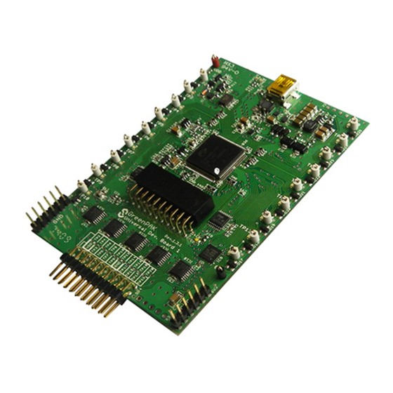
Page 6: Hardware
Note: All test points were designed only for observation of signals on the pins. Please do not try to connect external power/signal source to test points, this will affect GreenPAK Advanced Development Platform functionality and may even damage it. Silego Technology Inc. -
Page 7: Functional Description
3.2.6 Socket Connector The GreenPAK Advanced Development Platform should be used with a detachable socket board. Its main purpose is to connect the GreenPAK chip to the Development Platform. It‘s easy to use the programmed chip in external circuits, or to measure current consumption of the project. -
Page 8: Expansion Connector
3.2.7 Expansion Connector This port was designed to connect the GreenPAK Advanced Development Platform to external circuits and apply external power, signal sources and loads. It can be used to apply the GreenPAK chip into your custom design with minimal additional tools. For schematic diagram refer to Figure 3. - Page 9 When the Test mode button is pressed the software will first read the chip to verify if it was inserted and then configure the GreenPAK Advanced Development Platform as set in Emulation Tool window. When the Test mode button is gray then the Development Platform is in Default state and all expansion port switches are open (disconnected).
- Page 10 GreenPAK Advanced Development Platform The GreenPAK Advanced Development Platform provides three possible ways of using expansion connector: 1) Internal power is used to run the chip, no external power output is needed, external signal sources and loads can be connected between pins and GND.
-
Page 11: Pins Connectivity
Figure 8. Expansion Connector. Pin with Protection Resistor 3.2.8 Pins Connectivity The GreenPAK Advanced Development Platform supports connecting eight types of loads and signal sources. Each source has its own special purpose. The List of available connections for each test point is presented in the table below. - Page 12 GreenPAK Advanced Development Platform Pin signal sources/loading schematics: Silego Technology Inc. Page 11 of 41 08/15/17...
- Page 13 GreenPAK Advanced Development Platform Note*: VDD Signal generator works similar to other Signal generators but has wider output voltage range. It can provide maximum supply level of 5.5 V. Silego Technology Inc. Page 12 of 41 08/15/17...
-
Page 14: Example Projects Using Slg46721
4 Example Projects using SLG46721 4.1 Project: Counter with Clock Enable Blocks required: • 2 digital inputs • 1 digital output • 1 Look-Up table with two inputs • 1 Counter Figure 9. GreenPAK Designer Silego Technology Inc. Page 13 of 41 08/15/17... - Page 15 GreenPAK Advanced Development Platform Figure 10. GreenPAK Components List Silego Technology Inc. Page 14 of 41 08/15/17...
- Page 16 All components used in the project are shown in , next step is to configure selected blocks. Double click on PIN20 to open “Properties” panel. Select “1x push pull” from the drop-down menu in Pin20 properties and hit “Apply” button. Silego Technology Inc. Page 15 of 41 08/15/17...
- Page 17 (AND gate). Select AND gate from “Standard gates” drop-down menu or set table manually. Second Look-Up Table (LUT5) is configured as NOR gate. It is used to generate reset signal for counter on PIN3 falling edge. Silego Technology Inc. Page 16 of 41...
- Page 18 GreenPAK Advanced Development Platform Figure 12. Look-Up Table Properties Configured as AND Gate Silego Technology Inc. Page 17 of 41 08/15/17...
- Page 19 GreenPAK Advanced Development Platform Figure 13. Look-Up Table Properties Configured as NOR Gate Silego Technology Inc. Page 18 of 41 08/15/17...
- Page 20 The final step is to connect used components. Use Wire tool to perform this action. To connect two pins select “Set Wire” then click on the first and the second pin of the module or modules that you want to connect. The trace will be automatically routed. Silego Technology Inc. Page 19 of 41...
- Page 21 Figure 15 displays ready project with configured blocks and wire connections. Use the GreenPAK Advanced Development Platform to test this project. Connect the GreenPAK Advanced Development Platform to the PC and press “Emulation” button. This will load the code of your project to the chip and will enable Test functionality of your Development Platform.
- Page 22 Figure 18. Signal Generator Settings The purpose of the logic generator is to provide clock pulses for the Counter block. It is configured for 10 Hz clock source as shown in the Figure 19. Silego Technology Inc. Page 21 of 41 08/15/17...
- Page 23 Figure 19. Logic Generator Properties Functionality Waveform Channel 1 (yellow/top) – Logic generator Channel 2 (light blue/2nd line) – Button, 1 - enable Counter; 0 - disable Counter Channel 3 (magenta/3rd line) – Counter output Silego Technology Inc. Page 22 of 41 08/15/17...
- Page 24 Figure 21. Waveform, no Triggered on Button Released Channel 1 (yellow/top) – Logic generator Channel 2 (light blue/2nd line) – Button, 1 - enable Counter; 0 - disable Counter Channel 3 (magenta/3rd line) – Counter output Silego Technology Inc. Page 23 of 41 08/15/17...
-
Page 25: Project: Led String With Direction
4.2 Project: LED String with Direction For this project we will need: • Analog pin for input data • Digital pin for PWM output • ADC block • PWM block Figure 23. Used Blocks for Current Project Silego Technology Inc. Page 24 of 41 08/15/17... - Page 26 GreenPAK Advanced Development Platform For testing this project, the Signal generator with sine waveform is used. Figure 24. Sine Waveform Generated with Signal Generator Silego Technology Inc. Page 25 of 41 08/15/17...
- Page 27 Figure 25. Emulation Window, with Buffered LED and Signal Generator Pin configuration Pin # Pin Name Type Pin Description Supply Voltage DIRECTION Input Controls direction SIGNAL Input Analog Input Ground LED_A Output LED_B Output LED_C Output Silego Technology Inc. Page 26 of 41 08/15/17...
- Page 28 GreenPAK Advanced Development Platform Figure 26. Pin Properties Pin 6 is configured as analog input-output. This pin is used for generating SINE waveform. Silego Technology Inc. Page 27 of 41 08/15/17...
- Page 29 GreenPAK Advanced Development Platform Figure 27. Pin Properties Figure 28. Look-Up Tables Properties Configured as XOR Gate Silego Technology Inc. Page 28 of 41 08/15/17...
- Page 30 If Pin 2 logic level is set to “1”, these states will transform into: • All LEDs are on • LED_A and LED_B are on • LED_A is on • All LEDs are off Silego Technology Inc. Page 29 of 41 08/15/17...
- Page 31 Channel 1 (yellow/top) – Direction Channel 2 (light blue /2nd line) – LED_A Channel 3 (magenta/3rd line) – LED_B Channel 4 (blue / 4rth line) – LED_C Figure 31. LED Output with Direction (PIN2) Low Silego Technology Inc. Page 30 of 41 08/15/17...
- Page 32 GreenPAK Advanced Development Platform Figure 32. LED Output with Direction (PIN2) High The PWM duty cycle rises up to 100% when analog signal is close to 1 V. Silego Technology Inc. Page 31 of 41 08/15/17...
-
Page 33: Conclusion
This Development Platform is a truly versatile tool. It allows the designer to create a custom project within minutes, without using additional devices (except oscilloscope). For more information please visit our website http://www.silego.com/. Silego Technology Inc. Page 32 of 41... -
Page 34: Appendix A - Electrical Specification
Output Frequency (SINE) 0.01 2500 Max. Number of Points Sample Rate kSPS Output Level High Output Level Low Virtual Button, VDD/GND, Pull Up/Down Driver Strong Drive (VDD/GND) Resistance Pull Up/Down Resistance k Silego Technology Inc. Page 33 of 41 08/15/17... - Page 35 Max. Voltage Continuous Current through Any Terminal ±30 Switch On-Resistance External VDD Switch On-Resistance Expansion Connector Switch On Leakage Current Off Leakage Current Bandwidth Max. VDD Supply from External Source 5.66 Silego Technology Inc. Page 34 of 41 08/15/17...
-
Page 36: Appendix B - Schematic Diagram
GreenPAK Advanced Development Platform 6 Appendix B - Schematic Diagram Figure 33. MCU Silego Technology Inc. Page 35 of 41 08/15/17... - Page 37 GreenPAK Advanced Development Platform Figure 34. Analog Switches, Protection Diodes and LEDs Silego Technology Inc. Page 36 of 41 08/15/17...
- Page 38 GreenPAK Advanced Development Platform Figure 35. Socket and Expansion Connectors Figure 36. Signal Generators Silego Technology Inc. Page 37 of 41 08/15/17...
- Page 39 GreenPAK Advanced Development Platform Figure 37. Boost Converter USB Interface Figure 38. Port Extender Silego Technology Inc. Page 38 of 41 08/15/17...
- Page 40 GreenPAK Advanced Development Platform Figure 39. USB Protection Silego Technology Inc. Page 39 of 41 08/15/17...
-
Page 41: Appendix C - Bom
C46, C47, C48, C49, C50, C51, C54, Csoc EMK316BJ106KL-T 1206 (3216 Metric) C2, C3, C4, C7, C14, C26, C2012X7R1C105K/1.25 0805 (2012 Metric) C21, C29, C39, C45 CC0402KRX7R9BB103 0402 (1005 Metric) C5, C15, C52, C55 Silego Technology Inc. Page 40 of 41 08/15/17... - Page 42 RN1, RN2, RN3, RN4, 5000_ 5001_ 5002_ TP2-TP10, TP12-TP20 SJ61A6 TSW-110-08-L-D-RA 0.100" (2.54mm) SV4, SVsoc SSQ-110-02-T-D-RA 0.100" (2.54mm) 961106-6404-AR 0.100" (2.54mm) SV2, SV3 3021009-06 RESISTOR 0 1206 (3216 Metric) SLG55321 TDFN-8 BZV55C5V6-TP SOD-80C Silego Technology Inc. Page 41 of 41 08/15/17...
- Page 43 Programmable Logic IC Development Tools Click to view products by manufacturer: Silego Other Similar products are found below : HLDC-DDR3-A DK-DEV-5SGXEA7N EK-10M50F484 EPXA4F672C2 EPXA4F672C3 EPXA4F672C1 K0161 LCMXO256C-S-EVN 12GSDIFMCCD SFP+X4FMCCD 88980182 P0582 HW-PWAC-2600317 DEV-17514 LCMXO3D-9400HC-B-EVN P0671 DK-K7- CONN-G P0467 LCMXO2-1200ZE-P1-EVN LCMXO2-4000HE-DSIB-EVN DK-DEV-4SGX530N LCMXO3L-SMA-EVN P006-006-2...
Need help?
Do you have a question about the GreenPAK Advanced Development Platform and is the answer not in the manual?
Questions and answers