Table of Contents
Advertisement
SERVICE MANUAL
Ver. 1.2 2013.11
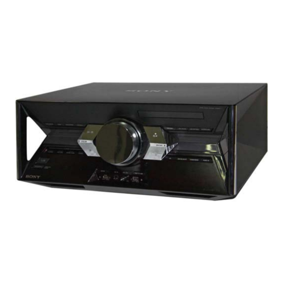
• HCD-SHAKE7 is the tuner, USB, CD player, Bluetooth, NFC
and amplifi er section in SHAKE-7.
Amplifi er section
The following are measured at
Mexican model:
AC 120 V – 240 V, 60 Hz
Other models:
AC 120 V – 240 V, 50/60 Hz
Tweeters/woofers
Power Output (rated):
320 W + 320 W (at 4 ohms, 1 kHz,
1% THD)
RMS output power (reference):
520 W + 520 W (per channel at
4 ohms, 1 kHz)
Mid speakers
Power Output (rated):
240 W + 240 W (at 5 ohms, 1 kHz,
1% THD)
RMS output power (reference):
385 W + 385 W (per channel at
5 ohms, 1 kHz)
Subwoofers
Power Output (rated):
320 W + 320 W (at 4 ohms, 100 Hz,
1% THD)
RMS output power (reference):
520 W + 520 W (per channel at
4 ohms, 100 Hz)
Inputs
TV/DVD/SAT (AUDIO IN) L/R
Voltage 2 V, impedance 47 kilohms
PC/GAME (AUDIO IN) L/R
Voltage 2 V, impedance 47 kilohms
MIC
Sensitivity 1 mV, impedance 10 kilohms
A (USB),
B (USB) port: Type A
USB section
Supported bit rate
WMA:
48 kbps – 192 kbps, VBR, CBR
AAC:
48 kbps – 320 kbps, VBR, CBR
Sampling frequencies
WMA: 44.1 kHz
AAC: 44.1 kHz
Supported USB device
Mass Storage Class
Maximum current
500 mA
9-890-619-03
Sony Corporation
2013K80-1
©
2013.11
Published by Sony EMCS (Malaysia) PG Tec
HCD-SHAKE7
Model Name Using Similar Mechanism
CD Section
CD Mechanism Type
Optical Pick-up Name
SPECIFICATIONS
Disc/USB section
Supported bit rate
MPEG1 Layer-3:
32 kbps – 320 kbps, VBR
MPEG2 Layer-3:
8 kbps – 160 kbps, VBR
MPEG1 Layer-2:
32 kbps – 384 kbps, VBR
Sampling frequencies
MPEG1 Layer-3:
32 kHz/44.1 kHz/48 kHz
MPEG2 Layer-3:
16 kHz/22.05 kHz/24 kHz
MPEG1 Layer-2:
32 kHz/44.1 kHz/48 kHz
Disc player section
System
Compact disc and digital audio system
Laser Diode Properties
Emission Duration: Continuous
Laser Output*: Less than 44.6 µW
* This output is the value
measurement at a distance of
200 mm from the objective lens
surface on the Optical Pick-up
Block with 7 mm aperture.
Frequency response
20 Hz – 20 kHz
Signal-to-noise ratio
More than 90 dB
Dynamic range
More than 88 dB
Tuner section
FM stereo, FM/AM superheterodyne tuner
Antenna:
FM lead antenna
AM loop antenna
FM tuner section
Tuning range
87.5 MHz – 108.0 MHz
(50 kHz step)
AM tuner section
Tuning range
Pan American models:
531 kHz – 1,710 kHz (9 kHz step)
530 kHz – 1,710 kHz (10 kHz step)
Saudi Arabian model:
531 kHz – 1,602 kHz (9 kHz step)
Other models:
531 kHz – 1,602 kHz (9 kHz step)
530 kHz – 1,610 kHz (10 kHz step)
Bluetooth section
Communication system
Bluetooth Standard version 3.0 +
EDR (Enhanced Date Rate)
Output
Bluetooth Standard Power Class 2
Maximum communication range
1)
Line of sight approx. 10m
Frequency band
2.4 GHz band (2.4000 GHz – 2.4835 GHz)
Modulation method
FHSS (Freq Hopping Spread Spectrum)
2)
Compatible Bluetooth profiles
A2DP (Advanced Audio Distribution
Profile)
AVRCP 1.3 (Audio Video Remote
Control Profile)
Supported codecs
SBC (Sub Band Codec)
AAC (Advanced Audio Coding)
1)
The actual range will vary depending on
factors such as obstacles between devices,
magnetic fields around a microwave oven,
static electricity, reception sensitivity,
antenna's performance, operating system,
software application, etc.
2)
Bluetooth standard profiles indicate the
purpose
of
Bluetooth
communication
between devices.
General
Power requirements
Mexican model:
AC 120 V – 240 V, 60 Hz
Other models:
AC 120 V – 240 V, 50/60 Hz
Power consumption
420 W
Dimensions (w/h/d) (excl. speakers)
(Approx.) (Except AR)
500 mm × 220 mm × 380 mm
MINI HI-FI COMPONENT SYSTEM
E Model
NEW
CDM90-DVBU202//M
CMS-S76RFS7G
Dimensions (w/h/d) (excl. speakers) (AR)
500 mm × 220 mm × 380 mm
Mass (excl. speakers) (Approx.) (Except AR)
8.4 kg
Mass (excl. speakers) (AR)
8.4 kg
Supplied accessories
Remote control (1)
R6 (Size AA) batteries (2)
FM lead/AM loop antenna (1)
Design and specifications are subject to
change without notice.
License and Trademark Notice
• "WALKMAN" and "WALKMAN" logo
are registered trademarks of Sony Corpo-
ration.
• MPEG Layer-3 audio coding technology
and patents licensed from Fraunhofer IIS
and Thomson.
• Windows Media is either a registered
trademark or trademark of Microsoft
Corporation in the United States and/or
other countries.
• This product is protected by certain
intellectual property rights of Microsoft
Corporation.
Use
or
distribution
of
such technology outside of this product
is prohibited without a license from
Microsoft or an authorized Microsoft
subsidiary.
• The Bluetooth® word mark and logos are
registered trademarks owned by Bluetooth
SIG, Inc. and any use of such marks by
Sony Corporation is under license. Other
trademarks and trade names are those of
their respective owners.
• The N Mark is a trademark or registered
trademark of NFC Forum, Inc. in the
United States and in other countries.
• Android is a trademark of Google Inc.
• All
other
trademarks
and
registered
trademarks are of their respective holders.
In this manual, ™ and ® marks are not
specified.
Advertisement
Table of Contents

Related Manuals for Sony HCD-SHAKE7


Summary of Contents for Sony HCD-SHAKE7
- Page 1 HCD-SHAKE7 SERVICE MANUAL E Model Ver. 1.2 2013.11 • HCD-SHAKE7 is the tuner, USB, CD player, Bluetooth, NFC and amplifi er section in SHAKE-7. Model Name Using Similar Mechanism CD Section CD Mechanism Type CDM90-DVBU202//M Optical Pick-up Name CMS-S76RFS7G SPECIFICATIONS Amplifi...
- Page 2 COMPONENTS IDENTIFIED BY MARK 0 OR DOTTED LINE WITH MARK 0 ON THE SCHEMATIC DIAGRAMS AND IN THE PARTS LIST ARE CRITICAL TO SAFE OPERATION. REPLACE THESE COMPONENTS WITH SONY PARTS WHOSE PART NUMBERS APPEAR AS SHOWN IN THIS MANUAL OR IN SUPPLEMENTS PUBLISHED BY SONY.
-
Page 3: Table Of Contents
HCD-SHAKE7 TABLE OF CONTENTS SERVICING NOTES ..........6-17. Printed Wiring Board - DISPLAY Board - ..... 40 6-18. Schematic Diagram - DISPLAY Board - ......41 DISASSEMBLY 6-19. Printed Wiring Board - VOLUME Board (Component Side) - ......42 2-1. Side-L Panel Assy, Side-R Panel Assy, Top Panel .. -
Page 4: Servicing Notes
HCD-SHAKE7 Ver. 1.2 SECTION 1 SERVICING NOTES Notes on chip component replacement MODEL IDENTIFICATION • Never reuse a disconnected chip component. - BACK PANEL - • Notice that the minus side of a tantalum capacitor may be damaged by heat. - Page 5 – you may have to press N twice. Bluetooth device. – you may need to start playback of an audio source on the For example, select “SONY SHAKE-7”. Bluetooth device. If passkey is required on the Bluetooth device, enter “0000”.
-
Page 6: Disassembly
HCD-SHAKE7 SECTION 2 DISASSEMBLY Note: Disassemble the unit in the order as shown below. 2-1. SIDE-L PANEL ASSY, SIDE-R PANEL ASSY, TOP PANEL (Page 7) 2-2. BACK PANEL SECTION (Page 8) 2-3. LOADING PANEL ASSY (Page 8) 2-4. CDM90-DVBU202//M (Page 9) 2-5. - Page 7 HCD-SHAKE7 Note: Follow the disassembly procedure in the numerical order given. 2-1. SIDE-L PANEL ASSY, SIDE-R PANEL ASSY, TOP PANEL 2 one screw (+BVTP 3 1 three screws 4 panel, top (+BVTP 3 2 one screw (+BVTP 3 5 four screws...
-
Page 8: Back Panel Section
HCD-SHAKE7 2-2. BACK PANEL SECTION 2 CN1000 (2P) 6 two screws (+BVTP 3 1 CN1001 (2P) 5 five screws (+BVTP 3 4 three screws (+BVTP 3 3 three screws (+BVTP 3 8 back panel section 2-3. LOADING PANEL ASSY hole –... -
Page 9: Cdm90-Dvbu202//M
HCD-SHAKE7 2-4. CDM90-DVBU202//M 4 four screws (+BVTP 3 5 boss 7 CDM90-DVBU202//M Note: When you install the BD drive (CDM90-DVBU202//M), please match the position of 3 wire (flat type) (5 core) the boss two places. (CN306) 1 wire (flat type) (24 core) -
Page 10: Motherboard Board
HCD-SHAKE7 2-6. MOTHERBOARD BOARD 3 two screws (+BVTP 3 5 three screws (+PTPWH 2.6 L (DIA8.0)) 4 bracket, tunnel 7 heat sink 6 thermal sheet 8 two screws (+BVTP 3 8 three screws (+BVTP 3 8 two screws (+BVTP 3... -
Page 11: Switching Regulator (Smg-1800)
HCD-SHAKE7 2-7. SWITCHING REGULATOR (SMG-1800) 1 six screws (+PWH 3 8 (SUMITITE)) 2 sub chassis 5 nine screws (+PWH 3 8 (SUMITITE)) 3 CN1 (2P) 6 REGULATOR, SWITCHING (SMG-1800) 7 chassis... -
Page 12: Service Optical Device, Wire (Flat Type)
HCD-SHAKE7 2-8. SERVICE OPTICAL DEVICE, WIRE (FLAT TYPE) Note 1 : Before disconnecting the wire (fl at type) (24 core) of optical pick-up block, solder the short-land. 2 chuck holder assy (T) 2 Solder the short-land. 1 six claws Note 2: When assembling the optical pick-up block, remove the solder of short-land after connecting the wire (flat type) (24 core). -
Page 13: Storm Test Mode
HCD-SHAKE7 SECTION 3 STORM TEST MODE [PANEL TEST MODE] [MODEL & DEST WRITE MODE] This mode is used to set software model & destination. This mode is used to check the fl uorescent indicator tube, LEDs, This mode is only available when no permanent model & destina- keys, [VOLUME / DJ CONTROL] jog, model, destination and tion is stored. - Page 14 HCD-SHAKE7 [USER RESET] [CDM AGING MODE] The user reset clears all data including preset data stored in the data This mode is used for CDM aging. fl ash to initial conditions exclude history mode data. Procedure: 1. Press button to turn on the system.
- Page 15 HCD-SHAKE7 Display Item Protector Count ※ ※ Protector Type (refer PROTECTOR KIND CHECK TEST MODE) Protector type Protector Error Code AMPL PWR2 ※ ※ ※ ※ TEMP Single Power On Time ※ ※ M ※ ※ ※ ※ ※ Total Power On Time ※...
-
Page 16: Electrical Check
HCD-SHAKE7 SECTION 4 ELECTRICAL CHECK TUNER SECTION 0 dB = 1 V FM AUTO STOP CHECK signal generator – Procedure: 1. Turn the power on. 2. Input the following signal from Signal Generator to FM antenna input directly. Carrier frequency : A = 87.5 MHz, B = 98 MHz, C = 108 MHz... -
Page 17: Troubleshooting
HCD-SHAKE7 SECTION 5 TROUBLESHOOTING... - Page 18 HCD-SHAKE7...
- Page 19 HCD-SHAKE7...
- Page 20 HCD-SHAKE7...
- Page 21 HCD-SHAKE7...
-
Page 22: Diagrams
HCD-SHAKE7 SECTION 6 DIAGRAMS • Circuit Boards Location SWITCHING REGULATOR (SMG-1800) MOTHERBOARD board MS-476 board VOLUME board MIC SUPPORT board BLUETOOTH module BUTTON_R board BUTTON_L board RGB BAR_L board RC-S801/A (WW) USB board MIC board RGB BAR_R board DISPLAY board... -
Page 23: Block Diagram - Rs Servo, Usb Section
HCD-SHAKE7 6-1. BLOCK DIAGRAM - RS SERVO, USB Section - RFIP VOA/A RF_C VOB/B RF_B VOC/C RF_A VOD/D RF_D XTALO 8 VOE/E+G RF_F X301 24MHz VOF/F+H RF_E 27MHz XTALI 7 MDI1 CN2201 AUTO LD(780) POWER CTRL LDO1 Q902 USB_DP 25... -
Page 24: Block Diagram - Main Section
HCD-SHAKE7 6-2. BLOCK DIAGRAM - MAIN Section - MIC DETECT Q2301, Q2302 STEREO A/D MIC AMP CONVERTER IC2301 IC654 J2301 VINL DOUT 9 MIC IN VINR BCK 8 RV2301 MIC VOL MIN MAX STEREO A/D STEREO D/A CONVERTER SIGNAL SELECTOR... -
Page 25: Block Diagram - Amp Section
HCD-SHAKE7 6-3. BLOCK DIAGRAM - AMP Section - POWER AMP +53V OP AMP IC1000 IC1012 DIGITAL AUDIO MOSFET TB1000 Q1041 AOUT VS 13 RESET SWITCH Q1012 DIGITAL AUDIO MOSFET Q1042 OP AMP SWITCH COM 10 IC658 Q1024 TWEETERS/WOOFERS TH1001 D1001... -
Page 26: Block Diagram - Panel, Power Supply Section
HCD-SHAKE7 6-4. BLOCK DIAGRAM - PANEL, POWER SUPPLY Section - LED +13.5V O-FL-SOUT VACUUM FLUORESCENT D2401 - D2404 O-FL-CLK DISPLAY DC-DC CONVERTER SWITCHING O-FL-LATCH TD FL ND2401 TRANSFORMER TRANSISTOR 26 O-FL-BK TUBE T2401 Q2403, Q2404 +1.2V REG. +3.3V REG. IC302... - Page 27 HCD-SHAKE7 Ver. 1.2 • Note for Printed Wiring Boards and Schematic Diagrams • Waveforms – MOTHERBOARD Board – Note on Printed Wiring Board: Note on Schematic Diagram: • X : parts extracted from the component side. • All capacitors are in μF unless otherwise noted. (p: pF) •...
-
Page 28: Printed Wiring Board - Motherboard Board (Component Side)
HCD-SHAKE7 Ver. 1.1 6-5. PRINTED WIRING BOARD - MOTHERBOARD Board (Component Side) - • See page 22 for Circuit Boards Location. • : Uses unleaded solder. MOTHERBOARD BOARD (COMPONENT SIDE) J651 AUDIO IN TB1002 TB1001 TB1000 SUBWOOFERS MID SPEAKERS TWEETERS/WOOFERS... -
Page 29: Printed Wiring Board - Motherboard Board (Conductor Side)
HCD-SHAKE7 6-6. PRINTED WIRING BOARD - MOTHERBOARD Board (Conductor Side) - • See page 22 for Circuit Boards Location. • : Uses unleaded solder. MOTHERBOARD BOARD (CONDUCTOR SIDE) SPEAKER Q1009, Q1045 B2 E2 JL196 JL195 JL194 JL280 JL281 JL658 JL657... -
Page 30: Motherboard Board (1/10)
HCD-SHAKE7 6-7. SCHEMATIC DIAGRAM - MOTHERBOARD Board (1/10) - • See page 27 for Waveforms. • See page 53 for IC Block Diagrams. MOTHERBOARD BOARD (3/10) MOTHERBOARD BOARD (1/10) R651 FE_3.3V_1 (Page 32) TAS-RESET C739 C802 MOTHERBOARD 10 16V TAS-INT DVDD3.3V... -
Page 31: Schematic Diagram - Motherboard Board (2/10)
HCD-SHAKE7 Ver. 1.1 6-8. SCHEMATIC DIAGRAM - MOTHERBOARD Board (2/10) - • See page 53 for IC Block Diagrams. • See page 62 for IC Pin Function Descriptions. MOTHERBOARD BOARD (1/10) MOTHERBOARD MOTHERBOARD BOARD (Page 30) BOARD IC302 MOTHERBOARD (2/10) (3/10) +1.2V REG. -
Page 32: Schematic Diagram - Motherboard Board (3/10)
HCD-SHAKE7 6-9. SCHEMATIC DIAGRAM - MOTHERBOARD Board (3/10) - • See page 53 for IC Block Diagrams. MOTHERBOARD BOARD (3/10) FE_DVD_LDD MOTHERBOARD BOARD R378 FB902 CL913 (1/10) FE_3.3V_1 (Page 30) MOTHERBOARD BOARD R901 (2/10) IC901 CL910 MM3464A33NRE (Page 31) R921... -
Page 33: Motherboard Board (4/10)
HCD-SHAKE7 6-10. SCHEMATIC DIAGRAM - MOTHERBOARD Board (4/10) - MOTHERBOARD BOARD (4/10) C1192 R1287 R1234 R1087 JL1035 JL1041 JL1008 C1241 C1196 R1077 SW-L 10 50V R1210 JL1038 120k C1320 R1421 -18.5 R1293 470p 4.7k 2.2k C1203 Q1045 R1118 C1037 C1306... -
Page 34: Motherboard Board (5/10)
POWER AMP (Page 38) C1304 R1105 IRF6775MTR1PBF 470p D1026, D1027 2.2k DIGITAL AUDIO C1159 C1348 C1349 R1348 JL1081 R1013 D1026 CRH02 (T5R, SONY, XM) MOSFET 4700 71V 0.015 0.01 4.7k 1 VAA C1212 C1328 R1302 D1027 C1277 C1020 0.01 R1071 R1375... -
Page 35: Motherboard Board (6/10)
HCD-SHAKE7 6-12. SCHEMATIC DIAGRAM - MOTHERBOARD Board (6/10) - MOTHERBOARD BOARD (4/10) (Page 33) MOTHERBOARD BOARD (6/10) Q1027 IC1006 2SC5053T100Q R1204 +18.5V REG. +5V REG. 20.6 18.5 JL1127 IC1006 R1093 D1006 KIA7805AF-RTF/PW BAV70 19.3 R1103 20.6 D1016 C1233 C1043 C1102... -
Page 36: Motherboard Board (7/10)
12 13 15 16 18 19 20 21 22 23 MOTHERBOARD BOARD (7/10) IC B/D R1462 IC1000 D1024, D1029 R1179 R1316 Q1041 CRH02 (T5R, SONY, XM) POWER AMP C1299 R1098 IRF6775MTR1PBF 470p JL1082 2.2k DIGITAL AUDIO C1158 C1356 C1357 R1355 R1017 0.015... -
Page 37: Motherboard Board (8/10)
HCD-SHAKE7 6-14. SCHEMATIC DIAGRAM - MOTHERBOARD Board (8/10) - • See page 27 for Waveforms. • See page 53 for IC Block Diagrams. • See page 62 for IC Pin Function Descriptions. MOTHERBOARD BOARD MOTHERBOARD BOARD (8/10) (1/10) DMB-AGND (Page 30) -
Page 38: Schematic Diagram - Motherboard Board (9/10)
HCD-SHAKE7 6-15. SCHEMATIC DIAGRAM - MOTHERBOARD Board (9/10) - • See page 27 for Waveforms. • See page 53 for IC Block Diagrams. MOTHERBOARD BOARD (9/10) JL106 JL117 SPICLK JL118 DATA JL119 JL120 JL121 JL123 RF-DET JL133 CN10 R177 JL162... -
Page 39: Motherboard Board (10/10)
HCD-SHAKE7 6-16. SCHEMATIC DIAGRAM - MOTHERBOARD Board (10/10) - • See page 53 for IC Block Diagrams. MOTHERBOARD BOARD MOTHERBOARD BOARD MOTHERBOARD BOARD (9/10) (9/10) (8/10) (Page 38) (Page 38) (Page 37) MOTHERBOARD BOARD (10/10) R142 R143 MOTHERBOARD BOARD MIC_IN... -
Page 40: Printed Wiring Board - Display Board
HCD-SHAKE7 6-17. PRINTED WIRING BOARD - DISPLAY Board - • See page 22 for Circuit Boards Location. • : Uses unleaded solder. BUTTON_R BOARD CN2003 (Page 47) DISPLAY BOARD ND2401 VACUUM FLUORESCENT DISPLAY CN2401 JL2402 JL2407 JL2404 JL2408 JL2403 JL2405... -
Page 41: Schematic Diagram - Display Board
HCD-SHAKE7 6-18. SCHEMATIC DIAGRAM - DISPLAY Board - DISPLAY BOARD ND2401 VACUUM FLUORESCENT DISPLAY 38 39 40 41 42 JL2410 JL2419 C2401 C2408 0.01 0.01 C2406 R2413 R2406 C2418 0.22 CN2401 C2417 D2401 ~ D2404 0.22 L2401 JL2409 CRH02 (T5R,SONY,XM) -
Page 42: Printed Wiring Board - Volume Board (Component Side)
HCD-SHAKE7 Ver. 1.1 6-19. PRINTED WIRING BOARD - VOLUME Board (Component Side) - • See page 22 for Circuit Boards Location. • : Uses unleaded solder. VOLUME BOARD (COMPONENT SIDE) BUTTON_R USB BOARD BOARD CN2203 CN2001 (Page 49) (Page 47) -
Page 43: Printed Wiring Board - Volume Board (Conductor Side)
HCD-SHAKE7 Ver. 1.1 6-20. PRINTED WIRING BOARD - VOLUME Board (Conductor Side) - • See page 22 for Circuit Boards Location. • : Uses unleaded solder. VOLUME BOARD (CONDUCTOR SIDE) JL2685 JL2686 JL2670 JL2660 JL2608 JL2624 JL2676 JL2622 JL2675 JL2672... -
Page 44: Schematic Diagram - Volume Board
HCD-SHAKE7 Ver. 1.1 6-21. SCHEMATIC DIAGRAM - VOLUME Board - • See page 53 for IC Block Diagrams. VOLUME BOARD NO2601 R2679 R2683 NO2602 R2694 R2644 R2668 JL2610 JL2660 LED 5.2V LED 5.2V R2678 R2685 R2692 JL2611 JL2661 R2676 R2687... -
Page 45: Printed Wiring Board - Button_L Board
HCD-SHAKE7 6-22. PRINTED WIRING BOARD - BUTTON_L Board - • See page 22 for Circuit Boards Location. • : Uses unleaded solder. BUTTON_L BOARD S2102 D2102 BLUETOOTH CONNECTION-PAIRING R2103 JL2102 JL2117 JL2101 JL2104 JL2115 JL2116 S2101 S2106 S2108 S2110 &/1... -
Page 46: Schematic Diagram - Button_L Board
HCD-SHAKE7 6-23. SCHEMATIC DIAGRAM - BUTTON_L Board - BUTTON_L BOARD NO2101 JL2114 LED 5.2V JL2115 AD-KEY0 JL2116 VOLUME DGND JL2117 LED1 BOARD JL2118 LED2 CN2603 JL2119 DJLED1 JL2120 (Page 44) DJLED2 JL2121 DJLED3 JL2122 DJLED4 R2102 S2103 S2105 S2107 S2109... -
Page 47: Printed Wiring Board - Button_R Board
HCD-SHAKE7 6-24. PRINTED WIRING BOARD - BUTTON_R Board - • See page 22 for Circuit Boards Location. • : Uses unleaded solder. BUTTON_R BOARD VOLUME DISPLAY MOTHERBOARD BOARD BOARD BOARD CN2601 CN2401 CN12 (Page 42) (Page 40) (Page 28) JL2056... -
Page 48: Schematic Diagram - Button_R Board
HCD-SHAKE7 6-25. SCHEMATIC DIAGRAM - BUTTON_R Board - 6-26. PRINTED WIRING BOARD - MIC Board - • • See page 22 for Circuit Boards Location. : Uses unleaded solder. J2301 MIC IN MOTHERBOARD BOARD (9/10) RV2301 CN12 MIC VOL (Page 38) -
Page 49: Schematic Diagram - Mic Board
HCD-SHAKE7 6-27. SCHEMATIC DIAGRAM - MIC Board - MIC BOARD C2314 R2315 C2322 C2302 D2301 R2302 1000p C2307 DA2J10100L R2306 JL2309 C2324 Q2301 R2316 LSAR523UBFS8TL C2317 JL2320 MIC DETECT 220p R2301 JL2306 R2314 C2319 JL2315 JL2313 1000p R2303 Q2302 R2309... -
Page 50: Schematic Diagram - Usb Board
HCD-SHAKE7 6-29. SCHEMATIC DIAGRAM - USB Board - USB BOARD D2201 1L0352B13F0MIT02 USB A R2203 CN2201 NO2201 JL2209 USB-A +5V PLAY MOTHERBOARD JL2204 JL2210 JL2205 JL2211 BOARD JL2212 5V 500mA USB-A GND (9/10) D2215 JL2213 DZ2J068M0L C2212 USB-B +5V JL2214... -
Page 51: Printed Wiring Boards - Rgb Bar Boards
HCD-SHAKE7 6-30. PRINTED WIRING BOARDS - RGB BAR Boards - • See page 22 for Circuit Boards Location. • : Uses unleaded solder. RGB BAR_R BOARD RGB BAR_L BOARD (COMPONENT SIDE) (COMPONENT SIDE) VOLUME BOARD VOLUME BOARD NO2601 NO2602 (Page 42) -
Page 52: Schematic Diagram - Rgb Bar Boards
HCD-SHAKE7 6-31. SCHEMATIC DIAGRAM - RGB BAR Boards - RGB BAR_L BOARD D1901 D1903 D1905 SMLVN6RGB1U17QYB SMLVN6RGB1U17QYB SMLVN6RGB1U17QYB CN1901 JL1919 LED 5.0V JL1917 RED_LED3 JL1915 BLUE_LED3 JL1913 GREEN_LED3 JL1911 VOLUME RED_LED2 JL1909 BLUE_LED2 BOARD JL1907 GREEN_LED2 NO2602 JL1905 RED_LED1 JL1903... - Page 53 HCD-SHAKE7 • IC Block Diagrams IC2 BU4829F-TR (MOTHERBOARD BOARD (8/10)) OUT 1 VDO 2 – Vref IC3 RN5B801-0002 (MOTHERBOARD BOARD (8/10)) IISD IISD VDDRF FM Antenna Digital Signal Process LOUT Filter Digital Stereo FRF1 Mixer Demodulator Decoder FM LNA ROUT...
- Page 54 HCD-SHAKE7 IC9 USX2064-AEZG-TR (MOTHERBOARD BOARD (9/10)) USBDM_DN1 USBDP_DN1 USBDM_DN2 USBDP_DN2 Bus- Serial 1.2 V reg power Interface Upstream detect/ USBDM_DN3 V bus pulse USBDP_DN3 Serial interface USBDM_DN4 Repeater Controller engine USBDP_DN4 TEST VDDCR Port PRTPWR1 controller 1.2 V reg OCS_N1...
- Page 55 HCD-SHAKE7 IC14 TC62D723FNG (MOTHERBOARD BOARD (9/10)) IC2601 TC62D723FNG (VOLUME BOARD) 25 GND Error detection result SIN 2 Output open/short detection circuit data register circuit 24 VDD SCK 3 TRANS 4 Constant current output circuit Reference voltage /OUT0 5 23 REXT...
- Page 56 HCD-SHAKE7 IC304 EM638165 TSB-6G (MOTHERBOARD BOARD (2/10)) VSS 54 DQ15 53 VSSQ 52 VDDQ CLOCK DQ14 51 BUFFER DQ13 50 VDDQ 49 VSSQ COLUMN DECODER DQ12 48 COLUMN DECODER CONTROL DQ11 47 SIGNAL COMMAND GENERATOR CELL ARRAY VSSQ 46 DECODER...
- Page 57 HCD-SHAKE7 IC651, IC652 PCM1754DBQR (MOTHERBOARD BOARD (1/10)) SYSTEM SYSTEM CLOCK 16 SCK CLOCK MANAGER AUDIO SERIAL DATA SERIAL CONTROL MUTE PORT PORT LRCK 13 DEMP DGND POWER 4x/8x OVERSAMPLING DIGITAL SUPPLY FILTER & FUNCTION CONTROL 12 TEST ENHANCED MULTILEVEL ZERO...
- Page 58 HCD-SHAKE7 IC654, IC655 PCM1808PWR (MOTHERBOARD BOARD (1/10)) LRCK Serial Interface Mode/ MOD0 Format MOD1 Control Clock SCKI Timing Control x1/64 Decimation Filter with High Pass Filter DGND Delta Sigma Delta Sigma Modulator Modulator DVDD Power Supply AVCC Antialias AGND AIN_L...
- Page 59 HCD-SHAKE7 IC656 TAS3108DCPR (MOTHERBOARD BOARD (1/10)) 20 19 AVSS VR_PLL ÷2 ÷2 XTALI MCLK XTALO MCLKI X 11 ÷2 ÷2 ÷ Z = 2 DEFAULT ÷4 ÷ X = 1 DEFAULT ÷ Y = 64 DEFAULT MCRCK_DV PLL and Clock Management...
- Page 60 HCD-SHAKE7 IC664 TC7WH157FK (MOTHERBOARD BOARD (1/10)) 11 7 11 6 SELECT EN G GND 4 IC902 AM5890S (MOTHERBOARD BOARD (3/10)) Vcc2 Voltage Detection MUTE Actuator Spindle Driver (6X) Driver (4X) Thermal Shut down Vcc2 Vcc2 Vcc1 Sled Actuator Driver (4X)
- Page 61 HCD-SHAKE7 IC1000, IC1005 IRS2092STRPBF-CU (MOTHERBOARD BOARD (7/10)) IC1001, IC1002, IC1003, IC1004 IRS2092STRPBF-CU (MOTHERBOARD BOARD (5/10)) FLOATING INPUT DETECT CLICK NOISE ELLIMINATION HIGH SIDE VAA+VSS COMP IN 3 PWM MODULATOR LEVEL SHIFT COMP 4 FLOATING HIGH SIDE LEVEL LEVEL SHIFT SHIFT...
- Page 62 HCD-SHAKE7 • IC Pin Function Descriptions MOTHERBOARD BOARD (8/10) IC11 R5F3650MCDFB (SYSTEM CONTROLLER) Pin No. Pin Name Description NO-USE Not used NO-USE Not used O-RGB-SOUT Serial data output to RGB driver I-SIRCS Remote control signal input O-RGB-SCLK Serial clock output to RGB driver...
- Page 63 HCD-SHAKE7 Pin No. Pin Name Description O-ANALOG-BSEL Multiplexer selector B for Analog input NO-USE Not used NO-USE Not used O-MTK-RESET MTK Reset pin I-MTK-XIFCS MTK CHIP SELECT O-MTK-BUSY BUSY Signal communication between MTK O-CD-MOTOR + CDM turning motor control signal output...
- Page 64 HCD-SHAKE7 MOTHERBOARD BOARD (2/10) IC306 CXD90013R (CD RF AMP FOCUS/TRACKING ERROR AMP CD SYSTEM PROCESSOR DIGITAL SERVO PROCESSOR Pin No. Pin Name Description RF main beam (A) input from the optical pick-up block RF main beam (D) input from the optical pick-up block...
- Page 65 HCD-SHAKE7 Pin No. Pin Name Description Two-way data bus with the SD-RAM DVDD12 Power supply terminal (+1.2V) Two-way data bus with the SD-RAM Two-way data bus with the SD-RAM Two-way data bus with the SD-RAM Two-way data bus with the SD-RAM...
- Page 66 HCD-SHAKE7 Pin No. Pin Name Description ADACVSS1 Ground terminal ARF/LFE Master clock signal output to the A/D converter and D/A converter Bit clock signal output to the A/D converter and D/A converter Not used AVCM Audio D/A converter reference voltage terminal...
-
Page 67: Exploded Views
HCD-SHAKE7 Ver. 1.2 SECTION 7 EXPLODED VIEWS Note: • The mechanical parts with no reference • Abbreviation The components identifi ed by mark 0 number in the exploded views are not sup- : Argentina model or dotted line with mark 0 are critical for : 120 V AC area in E model plied. -
Page 68: Back Panel Section
HCD-SHAKE7 7-2. BACK PANEL SECTION not supplied front panel section chassis section Ref. No. Part No. Description Remark 0 51 1-855-006-41 FAN, DC 7-685-646-71 SCREW +BVTP 3X8 TYPE2 IT-3... -
Page 69: Front Panel Section
HCD-SHAKE7 Ver. 1.2 7-3. FRONT PANEL SECTION not supplied not supplied (RGB BAR_L board) (BUTTON_L board) not supplied (VOLUME board) not supplied (RGB BAR_R board) not supplied not supplied (MIC SUPPORT board) supplied not supplied S2601 not supplied (MIC board) -
Page 70: Chassis Section
HCD-SHAKE7 Ver. 1.2 7-4. CHASSIS SECTION not supplied not supplied not supplied not supplied not supplied not supplied not supplied (E2, E51, E4) not supplied Ref. No. Part No. Description Remark Ref. No. Part No. Description Remark 4-435-965-01 SCREW+PTPWH 2.6XL (DIA8.0) -
Page 71: Cd Mechanism Section (Cdm90-Dvbu202//M)
HCD-SHAKE7 7-5. CD MECHANISM SECTION (CDM90-DVBU202//M) supplied (including MS-476 board) not supplied not supplied not supplied not supplied not supplied (MS-476 board) not supplied not supplied Note: If wire (fl at type) is replaced, install it after bending it in the same form as that before replacement. -
Page 72: Electrical Parts List
HCD-SHAKE7 Ver. 1.2 SECTION 8 BUTTON _ L BUTTON _ R ELECTRICAL PARTS LIST Note: • Items marked “*” are not stocked since • Abbreviation • Due to standardization, replacements in they are seldom required for routine ser- : Argentina model the parts list may be different from the vice. - Page 73 JR2032 1-216-864-11 SHORT CHIP JR2033 1-216-864-11 SHORT CHIP < DIODE > JR2034 1-216-864-11 SHORT CHIP D2401 6-503-775-01 DI CRH02 (T5R, SONY, XM) JR2035 1-216-864-11 SHORT CHIP D2402 6-503-775-01 DI CRH02 (T5R, SONY, XM) JR2036 1-216-864-11 SHORT CHIP D2403 6-503-775-01 DI CRH02 (T5R, SONY, XM)
- Page 74 HCD-SHAKE7 Ver. 1.2 MOTHERBOARD Ref. No. Part No. Description Remark Ref. No. Part No. Description Remark C2304 1-126-964-11 ELECT 10uF < VARIABLE RESISTOR > C2306 1-118-347-11 CERAMIC CHIP 0.1uF C2307 1-126-961-11 ELECT 2.2uF RV2301 1-227-452-11 RES, VAR, CARBON 50K (MIC VOL MIN MAX)
- Page 75 HCD-SHAKE7 Ver. 1.2 MOTHERBOARD Ref. No. Part No. Description Remark Ref. No. Part No. Description Remark 1-118-347-11 CERAMIC CHIP 0.1uF C119 1-162-961-11 CERAMIC CHIP 330PF 1-118-347-11 CERAMIC CHIP 0.1uF C129 1-164-850-11 CERAMIC CHIP 10PF 0.5PF 1-118-347-11 CERAMIC CHIP 0.1uF C130...
- Page 76 HCD-SHAKE7 Ver. 1.2 MOTHERBOARD Ref. No. Part No. Description Remark Ref. No. Part No. Description Remark C327 1-100-916-11 CERAMIC CHIP 0.1uF C684 1-112-300-91 CERAMIC CHIP 4.7uF C328 1-100-916-11 CERAMIC CHIP 0.1uF C685 1-112-300-91 CERAMIC CHIP 4.7uF C329 1-118-289-11 CERAMIC CHIP 0.1uF...
- Page 77 HCD-SHAKE7 Ver. 1.2 MOTHERBOARD Ref. No. Part No. Description Remark Ref. No. Part No. Description Remark C794 1-112-777-11 CERAMIC CHIP 0.01uF C1054 1-116-782-91 CERAMIC CHIP 2.2uF 100V C795 1-100-916-11 CERAMIC CHIP 0.1uF C1055 1-116-782-91 CERAMIC CHIP 2.2uF 100V C796 1-112-777-11 CERAMIC CHIP 0.01uF...
- Page 78 HCD-SHAKE7 Ver. 1.2 MOTHERBOARD Ref. No. Part No. Description Remark Ref. No. Part No. Description Remark C1165 1-118-118-91 CERAMIC CHIP 0.22uF 100V C1241 1-162-919-11 CERAMIC CHIP 22PF C1166 1-118-118-91 CERAMIC CHIP 0.22uF 100V C1242 1-162-915-11 CERAMIC CHIP 10PF 0.5PF C1167 1-118-118-91 CERAMIC CHIP 0.22uF...
- Page 79 DI DZ2J330M0L C1377 1-100-761-21 CERAMIC CHIP 0.01uF 250V C1378 1-100-761-21 CERAMIC CHIP 0.01uF 250V D1024 6-503-775-01 DI CRH02 (T5R, SONY, XM) C1379 1-114-324-11 CERAMIC CHIP 0.022uF D1025 6-503-775-01 DI CRH02 (T5R, SONY, XM) C1380 1-114-324-11 CERAMIC CHIP 0.022uF D1026 6-503-775-01...
- Page 80 HCD-SHAKE7 Ver. 1.2 MOTHERBOARD Ref. No. Part No. Description Remark Ref. No. Part No. Description Remark IC13 8-759-909-71 IC BA4558F < TRANSISTOR > IC14 6-719-142-01 IC TC62D723FNG IC302 6-712-033-01 IC MM1701CHBE 6-551-728-01 TRANSISTOR 2SB1710TL 6-550-363-01 TRANSISTOR 2SB1690KT146 IC304 (Not supplied)
- Page 81 HCD-SHAKE7 Ver. 1.2 MOTHERBOARD Ref. No. Part No. Description Remark Ref. No. Part No. Description Remark Q1050 6-552-891-01 LSAR523UBFS8TL 1-218-965-11 METAL CHIP 1/16W 1-218-941-81 METAL CHIP 1/16W Q1051 6-552-892-01 LSCR523UBFS8TL 1-218-941-81 METAL CHIP 1/16W Q1052 6-553-266-01 2PD601ART Q1055 6-553-266-01 2PD601ART...
- Page 82 HCD-SHAKE7 Ver. 1.2 MOTHERBOARD Ref. No. Part No. Description Remark Ref. No. Part No. Description Remark R134 1-218-965-11 METAL CHIP 1/16W R209 1-218-965-11 METAL CHIP 1/16W R135 1-218-965-11 METAL CHIP 1/16W R210 1-218-965-11 METAL CHIP 1/16W R136 1-218-965-11 METAL CHIP...
- Page 83 HCD-SHAKE7 Ver. 1.2 MOTHERBOARD Ref. No. Part No. Description Remark Ref. No. Part No. Description Remark R349 1-218-953-11 METAL CHIP 1/16W R690 1-218-929-11 METAL CHIP 1/16W R350 1-218-953-11 METAL CHIP 1/16W R691 1-218-929-11 METAL CHIP 1/16W R352 1-218-959-11 METAL CHIP 3.3K...
- Page 84 HCD-SHAKE7 Ver. 1.2 MOTHERBOARD Ref. No. Part No. Description Remark Ref. No. Part No. Description Remark R754 1-218-965-11 METAL CHIP 1/16W * R928 1-250-572-11 METAL CHIP 1/10W R755 1-218-965-11 METAL CHIP 1/16W * R929 1-250-572-11 METAL CHIP 1/10W R756 1-218-965-11...
- Page 85 HCD-SHAKE7 Ver. 1.2 MOTHERBOARD Ref. No. Part No. Description Remark Ref. No. Part No. Description Remark R1065 1-216-797-11 METAL CHIP 1/10W R1138 1-216-833-11 METAL CHIP 1/10W R1066 1-216-797-11 METAL CHIP 1/10W R1139 1-216-295-91 SHORT CHIP R1067 1-216-797-11 METAL CHIP 1/10W...
- Page 86 HCD-SHAKE7 Ver. 1.2 MOTHERBOARD Ref. No. Part No. Description Remark Ref. No. Part No. Description Remark R1226 1-216-864-11 SHORT CHIP R1312 1-216-843-11 METAL CHIP 1/10W R1227 1-216-864-11 SHORT CHIP R1313 1-216-843-11 METAL CHIP 1/10W R1230 1-216-864-11 SHORT CHIP R1314 1-216-843-11...
- Page 87 HCD-SHAKE7 Ver. 1.2 RGB BAR _ L RGB BAR _ R MOTHERBOARD MS-476 Ref. No. Part No. Description Remark Ref. No. Part No. Description Remark R1412 1-216-851-11 METAL CHIP 330K 1/10W < TERMINAL > R1415 1-216-295-91 SHORT CHIP R1418 1-216-796-11...
- Page 88 HCD-SHAKE7 Ver. 1.2 VOLUME Ref. No. Part No. Description Remark Ref. No. Part No. Description Remark C2206 1-118-347-11 CERAMIC CHIP 0.1uF S2202 1-762-875-21 SWITCH, TACTILE (ENTER) C2207 1-165-989-11 CERAMIC CHIP 10uF 6.3V ************************************************************* C2208 1-118-347-11 CERAMIC CHIP 0.1uF VOLUME BOARD...
- Page 89 HCD-SHAKE7 Ver. 1.2 VOLUME Ref. No. Part No. Description Remark Ref. No. Part No. Description Remark D2611 6-500-400-01 DIODE BAV99-215 R2653 1-216-805-11 METAL CHIP 1/10W D2612 6-500-400-01 DIODE BAV99-215 R2654 1-216-805-11 METAL CHIP 1/10W D2613 6-500-400-01 DIODE BAV99-215 R2655 1-216-805-11...
- Page 90 HCD-SHAKE7 Ver. 1.2 VOLUME Ref. No. Part No. Description Remark R2737 1-216-812-11 METAL CHIP 1/10W R2738 1-216-812-11 METAL CHIP 1/10W R2739 1-216-812-11 METAL CHIP 1/10W R2740 1-216-812-11 METAL CHIP 1/10W R2741 1-216-812-11 METAL CHIP 1/10W R2742 1-216-812-11 METAL CHIP 1/10W <...
- Page 91 HCD-SHAKE7 MEMO...
- Page 92 HCD-SHAKE7 REVISION HISTORY Checking the version allows you to jump to the revised page. Also, clicking the version at the top of the revised page allows you to jump to the next revised page. Ver. Date Description of Revision 2013.04 2013.08...
Need help?
Do you have a question about the HCD-SHAKE7 and is the answer not in the manual?
Questions and answers