Table of Contents
Advertisement
Quick Links
SERVICE MANUAL
Ver. 1.0 2008.04
• The tuner and CD sections have no adjustments.
CD Player section
Signal-to-noise ratio: 120 dB
Frequency response: 10 – 20,000 Hz
Wow and fl utter: Below measurable limit
Tuner section
FM
Tuning range:
87.5 – 108.0 MHz (at 50 kHz step)
87.5 – 107.9 MHz (at 200 kHz step)
FM tuning interval:
50 kHz/200 kHz switchable
Antenna (aerial) terminal:
External antenna (aerial) connector
Intermediate frequency: 10.7 MHz/450 kHz
Usable sensitivity: 9 dBf
Selectivity: 75 dB at 400 kHz
Signal-to-noise ratio:
67 dB (stereo), 69 dB (mono)
Harmonic distortion at 1 kHz:
0.5 % (stereo), 0.3 % (mono)
Separation: 35 dB at 1 kHz
Frequency response: 30 – 15,000 Hz
MW
Tuning range:
531 – 1,602 kHz (at 9 kHz step)
530 – 1,710 kHz (at 10 kHz step)
Sony Corporation
9-889-086-01
2008D04-1
Audio Business Group
©
2008.04
Published by Sony Techno Create Corporation
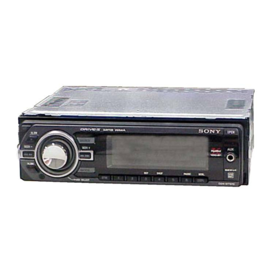
CDX-GT572
Model Name Using Similar Mechanism
CD Drive Mechanism Type
Optical Pick-up Name
SPECIFICATIONS
MW tuning interval:
9 kHz/10 kHz switchable
Antenna (aerial) terminal:
External antenna (aerial) connector
Intermediate frequency: 10.7 MHz/450 kHz
Sensitivity: 30 μV
SW
Tuning range:
SW1: 2,940 – 7,735 kHz
SW2: 9,500 – 18,135 kHz
(except for 10,140 – 11,500 kHz)
Antenna (aerial) terminal:
External antenna (aerial) connector
Intermediate frequency: 10.7 MHz/450 kHz
Sensitivity: 30 μV
Power amplifi er section
Outputs: Speaker outputs (sure seal connectors)
Speaker impedance: 4 – 8 ohms
Maximum power output: 52 W × 4 (at 4 ohms)
General
Output:
Audio outputs terminal (front/rear)
Subwoofer output terminal (mono)
Power antenna (aerial) relay control terminal
Power amplifi er control terminal
FM/MW/SW COMPACT DISC PLAYER
E Model
CDX-GT527EE/
GT570/GT570S
MG-101TC-188//Q
DAX-25A
Inputs:
BUS control input terminal
BUS audio input terminal
Remote controller input terminal
Antenna (aerial) input terminal
AUX input jack (stereo mini jack)
Tone controls:
Low: ±10 dB at 60 Hz (XPLOD)
Mid: ±10 dB at 1 kHz (XPLOD)
High: ±10 dB at 10 kHz (XPLOD)
Power requirements: 12 V DC car battery
(negative ground (earth))
Dimensions: Approx. 178 × 50 × 180 mm
1
1
(7
/
× 2 × 7
/
in.) (w/h/d)
8
8
Mounting dimensions: Approx.
182 × 53 × 162 mm
1
1
1
(7
/
× 2
/
× 6
/
in.) (w/h/d)
4
8
2
Mass: Approx. 1.2 kg (2 lb 11 oz)
Supplied accessories:
Card remote commander: RM-X151
Parts for installation and connections (1 set)
Design and specifi cations are subject to change
without notice.
Advertisement
Table of Contents

Related Manuals for Sony CDX-GT572


Summary of Contents for Sony CDX-GT572
- Page 1 531 – 1,602 kHz (at 9 kHz step) Power amplifi er control terminal 530 – 1,710 kHz (at 10 kHz step) FM/MW/SW COMPACT DISC PLAYER Sony Corporation 9-889-086-01 2008D04-1 Audio Business Group © 2008.04 Published by Sony Techno Create Corporation...
- Page 2 COMPONENTS IDENTIFIED BY MARK 0 OR DOTTED LINE WITH MARK 0 ON THE SCHEMATIC DIAGRAMS AND IN THE PARTS LIST ARE CRITICAL TO SAFE OPERATION. REPLACE THESE COMPONENTS WITH SONY PARTS WHOSE PART NUMBERS APPEAR AS SHOWN IN THIS MANUAL OR IN SUPPLEMENTS PUBLISHED BY SONY.
-
Page 3: Table Of Contents
CDX-GT572 TABLE OF CONTENTS SERVICE NOTE DIAGRAMS ............. 5-1. Block Diagram –Main Section– ........17 GENERAL 5-2. Block Diagram –Display Section– ......... 18 5-3. Printed Wiring Board –Main Section– ......19 Location of Controls ............5-4. Schematic Diagram –Main Section (1/3)– ...... 20 Connections .............. -
Page 4: Service Note
CDX-GT572 SECTION 1 SERVICE NOTE EXTENSION CABLE AND SERVICE POSITION When repairing or servicing this set, connect the jig (extension cable) as shown below. • Connect the MAIN board (CN350) and the SERVO board (CN2) with the extension cable (Part No. J-2502-076-1). -
Page 5: General
CDX-GT572 SECTION 2 This section is extracted GENERAL from instruction manual. • LOCATION OF CONTROLS Location of contr o ls and basic operations Main unit F OPEN button page 5 The following buttons on the card remote commander have also different buttons/functions G ALBM +/–... - Page 6 CDX-GT572 RCA pin cord (not supplied) Insert with the cord upwards. Cable con terminales RCA (no suministrado) Insertar con el cable hacia arriba. FRONT REMOTE SUB OUT (MONO) AUDIO OUT BUS AUDIO IN REAR FRONT AUDIO OUT from car antenna (aerial) desde la antena del automóvil...
-
Page 7: Disassembly
CDX-GT572 SECTION 3 DISASSEMBLY • This set can be disassembled in the order shown below. 3-1. SUB PANEL ASSY (Page 8) 3-2. CD MECHANISM BLOCK (Page 8) 3-4. SERVO BOARD 3-3. MAIN BOARD (Page 9) (Page 9) 3-5. CHASSIS (T) SUB ASSY (Page 10) 3-6. - Page 8 CDX-GT572 Note: Follow the disassembly procedure in the numerical order given. 3-1. SUB PANEL ASSY two claws two claws flexible flat cable (17 core) two screws (CN702) (+PTT 2.6 × 6) sub panel assy 3-2. CD MECHANISM BLOCK bracket (CD)
-
Page 9: Main Board
CDX-GT572 3-3. MAIN BOARD screw two screws screw (+PTT 2.6 × 10) (+P 2.6 × 8) (+PTT 2.6 × 8) two screws (+PTT 2.6 × 10) two screws (+P 2.6 × 8) cord (RCA) three ground point screws (+PTT 2.6 × 6) two screws (+PTT 2.6 ×... -
Page 10: Chassis (T) Sub Assy
CDX-GT572 3-5. CHASSIS (T) SUB ASSY two precision screws two precision screws (+P 1.7 × 2.2) (+P 1.7 × 2.2) chassis (T) sub assy claw 3-6. ROLLER ARM ASSY roller arm assy gear (RA1) spring (RAL) washer spring (RAR) -
Page 11: Chassis (Op) Assy
CDX-GT572 3-7. CHASSIS (OP) ASSY chassis (OP) assy tension spring (KF) coil spring (damper) (natural) coil spring (damper) (blue) slider (R) lever (D) gear (LE1) 3-8. CHUCKING ARM SUB ASSY chucking arm sub assy spring Note: Have this portion receive the chassis. -
Page 12: Sled Motor Assy
CDX-GT572 3-9. SLED MOTOR ASSY three serration screws (M 2 × 3) sled motor assy spring turn table spring stand Note: Never remove these parts since they were adjusted. stand Note: Place the stand with care not to touch the turn table. -
Page 13: Optical Pick-Up Section
CDX-GT572 3-10. OPTICAL PICK-UP SECTION optical pick-up section Note: Be careful not to touch the lens and hologram terminal when removing the optical pick-up section. 3-11. OPTICAL PICK-UP pan tapping screw (M 1.4 × 2.5) leaf spring (sub guide) leaf spring (OP) -
Page 14: Diagnosis Function
CDX-GT572 SECTION 4 DIAGNOSIS FUNCTION Description of the Diagnostics function: 4-3. Number of connected units display mode 1. Setting the Diag display mode With the power off, press the [4/SHUF] button, [5] button, and [4/SHUF] button on the set body or the remote control (for Shown the number of connected more than 2 seconds) in turn. - Page 15 CDX-GT572 4-5-2. Disc type and operating hours 4-6. OFFSET/FAILURE error display mode Operating hours Operating hours Disc type Error description (0: OFFSET, 1: FAILURE) Recency of information Recency of information 1 - 3: 1 represents the latest. 1 - 3: 1 represents the latest.
-
Page 16: Diagrams
CDX-GT572 SECTION 5 DIAGRAMS THIS NOTE IS COMMON FOR PRINTED WIRING BOARDS AND SCHEMATIC DIAGRAMS. (In addition to this, the necessary note is printed in each block.) For Schematic Diagram. For Printed Wiring Boards. Note: Note: • All capacitors are in μF unless otherwise noted. (p: pF) •... -
Page 17: Block Diagram -Main Section
CDX-GT572 5-1. BLOCK DIAGRAM – MAIN Section – SUB OUT ELECTRONIC VOLUME (MONO) IC401 J451 (1/2) J451 (2/2) 2 A2 R-CH 1 A1 AUDIO R-CH FRONT AUDIO OUT R-CH R-CH J901 9 DP2 OUTS2 R-CH 7 DP1 REAR AUDIO OUT... -
Page 18: Block Diagram -Display Section
CDX-GT572 5-2. BLOCK DIAGRAM – DISPLAY Section – SYSTEM CONTROL LCD DRIVER/LED CONTROL IC501 (2/2) IC901 71 RC_IN1 J370 REMOTE 43 RC_IN0 LCD_SO LCD901 LCD_CKO D501 LIQUID LCD_CE CRYSTAL DISPLAY COM1 PANEL COM4 KEYIN1 KEY MATRIX LED930,931 S901–915 LCD BACK... -
Page 19: Printed Wiring Board -Main Section
CDX-GT572 5-3. PRINTED WIRING BOARD – MAIN Section – • : Uses unleaded solder. J451 J370 CNJ400 CN300 • Semiconductor JW123 C442 C422 Location C432 C452 C323 C324 C414 C413 FU601 Ref. No. Location R432 R452 R442 R422 IC300 C305... -
Page 20: Schematic Diagram -Main Section (1/3)
CDX-GT572 5-4. SCHEMATIC DIAGRAM – MAIN Section (1/3) – • See page 26 for IC Block Diagrams. C323 C303 C306 C324 C308 C317 JC302 JC300 JC301 C301 C309 R302 JC504 C319 C304 C305 C307 R301 C318 IC300 IC/BD CN300 C465... -
Page 21: Schematic Diagram -Main Section (2/3)
CDX-GT572 5-5. SCHEMATIC DIAGRAM – MAIN Section (2/3) – • See page 26 for IC Block Diagrams. J451 CN410 C432 C442 C422 C452 C411 C413 C414 R411 R442 R422 R452 R432 R418 R416 JW25 C443 C447 R419 R417 R474 C423... -
Page 22: Schematic Diagram -Main Section (3/3)
CDX-GT572 5-6. SCHEMATIC DIAGRAM – MAIN Section (3/3) – • See page 16 for waveforms. • See page 27 for IC Pin Function Description of IC501. (Page 21) (Page 20) Q590 IC502 C519 R543 D493 Q589 S103 JC53 IC602 C501... -
Page 23: 5-7. Printed Wiring Boards -Sub Section
CDX-GT572 5-7. PRINTED WIRING BOARD – SUB Section – 5-8. SCHEMATIC DIAGRAM – SUB Section – • : Uses unleaded solder. (Page 24) LED202 R202 (Page 22) (Page 25) CN201 R201 LED201 S201 (12) (Page 19) CN202 (12) CDX-GT572... -
Page 24: 5-9. Printed Wiring Boards -Key Section
CDX-GT572 5-9. PRINTED WIRING BOARD – KEY Section – • : Uses unleaded solder. S901 LED958 D982 LED930 LED931 LED949 LCD901 LED951 S906 S903 LED956 S905 S911 S909 S913 S914 S912 S910 S908 S915 IC971 (12) (12) • Semiconductor Location Ref. -
Page 25: Schematic Diagram -Key Section
CDX-GT572 5-10. SCHEMATIC DIAGRAM – KEY Section – R981 D982 R977 R982 LED965 LED961 LED946 LED952 LED958 IC971 R978 LED963 LED959 LED993 LED955 LED957 LED931 R979 C971 LED962 LED966 LED949 LED954 LED956 R984 C981 IC901 C982 LED964 LED960 LED951 LED953... - Page 26 CDX-GT572 • IC Block Diagrams IC300 TDA8588AJ/N2/R1 (MAIN Board (1/3)) IC601 BA8271F-E2 (MAIN Board (1/3)) IC401 BD3442FS-E2 (MAIN Board (2/3)) BUS ON BUS.ON SWITCH VCC2 32 FIL LF– C BUS RESET 100k SWITCH 31 GND BUS.IN CLK-IN BATTERY INPUT INPUT...
- Page 27 CDX-GT572 • IC Pin Function Description IC501 MB90F045PF-G-9060-SPE1 (SYSTEM CONTROL) (MAIN BOARD (3/3)) Pin No. Pin Name Description AREASEL0 Destination setting pin 0 (Fixed at L in this set) AREASEL1 Destination setting pin 1 (Fixed at L in this set)
- Page 28 CDX-GT572 Pin No. Pin Name Description DAVN RDS data block synchronized detect signal input Not used in this set. (Pull down) Not used. (Open) UNISI S-BUS data signal input UNISO S-BUS data signal output UNISCK S-BUS clock signal output 61 to 63 Not used.
-
Page 29: Exploded Views
CDX-GT572 SECTION 6 EXPLODED VIEWS Note: • -XX and -X mean standardized parts, so • The mechanical parts with no reference The components identifi ed by mark 0 they may have some difference from the number in the exploded views are not sup- or dotted line with mark 0 are critical for original one. -
Page 30: Front Panel Section
CDX-GT572 6-2. FRONT PANEL SECTION RE901 not supplied LCD901 not supplied (KEY board) J901 not supplied not supplied not supplied not supplied Ref. No. Part No. Description Remark Ref. No. Part No. Description Remark A-1548-032-A PANEL OVERALL ASSY, FRONT 3-250-543-21... -
Page 31: Cd Mechanism Section (Mg-101Tc-188//Q)
CDX-GT572 6-3. CD MECHANISM SECTION (MG-101TC-188//Q) not supplied not supplied not supplied not supplied not supplied not supplied not supplied not supplied not supplied not supplied not supplied Ref. No. Part No. Description Remark Ref. No. Part No. Description Remark... -
Page 32: Electrical Parts List
CDX-GT572 SECTION 7 ELECTRICAL PARTS LIST Note: • Due to standardization, replacements in • RESISTORS When indicating parts by reference num- the parts list may be different from the All resistors are in ohms. ber, please include the board name. - Page 33 CDX-GT572 MAIN Ref. No. Part No. Description Remark Ref. No. Part No. Description Remark R917 1-216-825-11 METAL CHIP 2.2K 1/10W A-1312-912-A MAIN BOARD, COMPLETE R922 1-216-030-00 RES-CHIP 1/10W ******************** R924 1-216-031-00 RES-CHIP 1/10W R926 1-216-030-00 RES-CHIP 1/10W 7-685-134-19 SCREW +P 2.6X8 TYPE2 NON-SLIT...
- Page 34 CDX-GT572 MAIN Ref. No. Part No. Description Remark Ref. No. Part No. Description Remark C411 1-162-927-11 CERAMIC CHIP 100PF < CONNECTOR > C412 1-162-970-11 CERAMIC CHIP 0.01uF C413 1-163-251-11 CERAMIC CHIP 100PF CN300 1-774-701-21 PIN, CONNECTOR 16P C414 1-163-251-11 CERAMIC CHIP 100PF...
- Page 35 CDX-GT572 MAIN Ref. No. Part No. Description Remark Ref. No. Part No. Description Remark < IC > Q491 8-729-027-23 TRANSISTOR DTA114EKA-T146 Q492 8-729-027-43 TRANSISTOR DTC114EKA-T146 IC300 6-705-359-02 IC TDA8588AJ/N2/R1 Q501 8-729-027-23 TRANSISTOR DTA114EKA-T146 IC401 6-710-065-01 IC BD3442FS-E2 Q589 8-729-027-43 TRANSISTOR DTC114EKA-T146...
- Page 36 CDX-GT572 MAIN SERVO Ref. No. Part No. Description Remark Ref. No. Part No. Description Remark R491 1-216-805-11 METAL CHIP 1/10W R584 1-216-845-11 METAL CHIP 100K 1/10W R494 1-216-825-11 METAL CHIP 2.2K 1/10W R601 1-216-851-11 METAL CHIP 330K 1/10W R500 1-216-817-11...
- Page 37 CDX-GT572 Ref. No. Part No. Description Remark MISCELLANEOUS ************** 1-834-507-11 CABLE, FLEXIBLE FLAT (17 CORE) (CN202) 1-833-974-21 CONNECTION CORD FOR AUTOMOBILE (POWER) 1-833-887-11 CONNECTION CORD (RCA) (SUB OUT (MONO)) 0 103 X-2149-672-1 SERVICE ASSY, OP (DAX-25A) FU601 1-532-877-11 FUSE (BLADE TYPE) (AUTO FUSE) 10A...
- Page 38 CDX-GT572 REVISION HISTORY Checking the version allows you to jump to the revised page. Also, clicking the version at the top of the revised page allows you to jump to the next revised page. Ver. Date Description of Revision 2008.04...
Need help?
Do you have a question about the CDX-GT572 and is the answer not in the manual?
Questions and answers