Table of Contents

Related Manuals for Panasonic KX-TG2226B


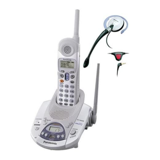
Summary of Contents for Panasonic KX-TG2226B
- Page 1 ORDER NO. KM40305083C1 Telephone Equipment KX-TG2226B / KX-TG2226S / KX-TG2226W / KX-TGA226B / KX-TGA226S / KX-TGA226W 2.4GHz Digital Cordless Answering System Black Version Silver Version White Version (for U.S.A.) SPECIFICATIONS...
-
Page 2: About Lead Free Solder (Pbf: Pb Free)
2003 Panasonic Communications Co., Ltd. All rights reserved. Unauthorized copying and distribution is a violation of law. 1. ABOUT LEAD FREE SOLDER (PbF: Pb free) Note: In the information below, Pb, the symbol for lead in the periodic table of elements, will refer to standard solder or solder that contains lead. -
Page 3: Suggested Pbf Solder
not to heat too long. - PbF solder will tend to splash if it is heated much higher than its melting point, approximately 1100°F, (600°C). - If you must use Pb solder on a PCB manufactured using PbF solder, remove as much of the original PbF solder as possible and be sure that any remaining is melted prior to applying the Pb solder. -
Page 4: For Service Technicians
Note: The locations of the “PbF“ mark are subject to change without notice. 1.2.2. Handset (Component View) Note: The locations of the “PbF“ mark are subject to change without notice. 2. FOR SERVICE TECHNICIANS ICs and LSIs are vulnerable to static electricity. When repairing, the following precautions will help prevent recurring malfunctions. -
Page 5: Battery Charge
4.2. Battery Charge 4.3. Battery Recharge Note for Service: The battery strength may not be indicated correctly if the battery is disconnected and connected again, even after it is fully charged. In that case, by recharging the battery as mentioned above, you will get a correct indication of the battery strength. -
Page 6: Location Of Controls
4.5. Battery Replacement 4.6. Battery information 5. LOCATION OF CONTROLS 5.1. Base Unit... - Page 7 5.2. Handset...
- Page 8 6. DISPLAY 6.1. Troubleshooting...
-
Page 13: Openlcr Service For Caller Iq Feature
- If you have any questions regarding the openLCR service, call openLCR's customer service department at 1-866-openLCR (1-866- 673-6527). - NEITHER PANASONIC COMMUNICATIONS CO., LTD. (PCC) NOR MATSUSHITA ELECTRIC CORPORATION OF AMERICA (MECA) IS IN ANY WAY AFFILIATED WITH, OR RESPONSIBLE FOR THE ACTS OR OMISSIONS OF, OPENLCR.COM, INC. -
Page 14: Downloading Phone Book Data
7.2. Downloading Phone Book Data... - Page 16 7.3. Information Download (Handset)
- Page 17 8. SETTINGS 8.1. Connections 8.2. Display Language...
- Page 18 8.3. Dialing Mode (Handset) 8.4. Direct Commands...
- Page 19 9. OPERATIONS 9.1. Making Calls (Handset)
- Page 22 9.2. Answering Calls (Handset) 9.3. FLASH Button (Handset)
-
Page 23: Erasing Messages
9.4. Erasing Messages... - Page 24 9.5. Phone Book You can store up to 50 names and phone numbers in the handset phone book. All phone book items are sorted alphabetically. You can make a call by selecting a name on the handset display. 9.5.1. Storing Names and Numbers (Handset)
- Page 26 9.5.2. Dialing from the Phone Book (Handset)
- Page 27 9.5.3. Editing an Item in the Phone Book (Handset)
- Page 28 9.5.4. Erasing an Item in the Phone Book (Handset) 10. DISASSEMBLY INSTRUCTIONS...
- Page 29 Shown in Fig.- To Remove - Remove - Lower Cabinet Screws (2.6 × 14)..(A) × 4 Main P.C. Board Tape and Solder Main P.C. Board Operational P.C. Board Screws (2.6 × 8)...(B) × 5 Operational P.C. Board...
- Page 30 Shown in Fig.- To Remove - Remove - Battery Cover Battery Cover Rear Cabinet Screw (2.6 × 12)..(C) × 1 Screws (2 × 14)..(D) × 2 Screws (2.6 × 12)..(E) × 2 Rear Cabinet Rear Cabinet Main P.C. Board Screw (2.6 × 12)..(F) × 1 Screws (2 ×...
-
Page 31: Troubleshooting Guide
11. ASSEMBLY INSTRUCTIONS 11.1. Fix the LCD to P.C. Board (Handset) 12. TROUBLESHOOTING GUIDE... -
Page 32: Check Power
Cross Reference: Check Power Error Message Table Check Playback Check Record Check Battery Charge Check Link Check the RF Unit Check Handset Transmission Check Handset Reception Check Caller ID 12.1. Check Power... -
Page 33: Error Message Table
Cross Reference: Power Supply Circuit Reset Circuit Note: Flash Memory is IC300. DSP is IC201. 12.2. Error Message Table... -
Page 34: Check Record
Display Symptom Remedy 1. Check the peripheral circuit of Flash Memory visually. The initialization was tried, but it could not be 2. Confirm that the voltage is added to the power supply pin. done. If no voltage is detected, replace the Flash Memory because it When the adjustment data was checked, an error be defect. - Page 35 How to change the Auto Disconnect activation (time) Some Telephone Company lines (fiber or cable) ON Hook and OFF Hook voltages are lower than conventional lines, which may cause a malfunction of Auto Disconnect detection.To solve this problem, try changing the Auto Disconnect activation (time) through the procedures below. Auto Disconnect activation (time) PROCEDURE Status...
-
Page 36: Check Playback
Flash Memory is IC300. DSP is IC201. 12.4. Check Playback Cross Reference: Power Supply Circuit Note: Flash Memory is IC300. DSP is IC201. 12.5. Check Battery Charge... -
Page 37: Check Link
12.6. Check Link... - Page 38 Cross Reference: Check the RF Unit Power Supply Circuit Note: Flash Memory is IC300. DSP is IC201. Cross Reference: Check the RF Unit Power Supply Circuit Note: EEPROM is IC202. DSP is IC201. 12.7. Check the RF Unit 12.7.1. Defective Unit Check The defective unit should be checked using the HS of Regular unit (working) and BS of Regular unit (working).
- Page 39 RF Check Flowchart Check Table for RF Block Note: *KX-TG2258 with marks HS JIG/BS JIG can be used only for troubleshooting. However, regular production set also can be used as a JIG. 12.7.2. Converting a Regular Production Unit to a JIG Both base unit and handset unit have two modes: TEST POWER LOW mode and NORMAL POWER mode even a Regular production unit.
- Page 40 b) BASE UNIT A short beep followed by a long beep is heard. This indicates the unit is in TEST POWER LOW mode. Once in TEST POWER LOW mode, to return the unit to the original NORMAL POWER mode, press 2, 5, 8, 0 simultaneously while the handset unit is in stand-by (not in use, not charging).
- Page 41 Fixation CH Figure 1 POWER making key “LOW“ "Soft Left key" + "1" “LOW“ "Soft Left key" + "2" “LOW“ "Soft Left key" + "3" “LOW“ "Soft Left key" + "4" “LOW“ "Soft Left key" + "5" “LOW“ "Soft Left key" + "6" “LOW“...
- Page 42 12.7.3. RF Check Flowchart : Details of confirmation items are following in “Check Table for RF Block ()”. Note: DSP is IC201. (for Base Unit) DSP is IC201. (for Handset) Both of RF Blocks for Handset and Base Unit are same. 12.7.4.
- Page 43 Item BS (Base unit) (*1) HS (Handset) (*1) 1. Put “HS (working)” on BS. 1. Put HS on “BS (working)”. 1a. Link Procedure77 2. Set MODE to [NORMAL POWER] of “HS 2. Set MODE to [NORMAL POWER] of “BS confirmation (working)“.
- Page 44 CIRCUIT BOARD (BASE UNIT) CIRCUIT BOARD (Handset) (*5)See Base Unit Reference Drawing (*6) see Handset Reference Drawing (*7) see Test mode flow chart for Base Unit (*8) see Test mode flow chart for Handset Note: DSP is IC201. (for Base Unit) DSP is IC201.
-
Page 45: Check Handset Transmission
12.8. Check Handset Transmission Cross Reference: SIGNAL ROUTE... -
Page 46: Test Mode
12.9. Check Handset Reception Cross Reference: SIGNAL ROUTE Note: When checking the RF UNIT, Refer to Check the RF Unit 12.10. Check Caller ID Cross Reference: Telephone Line Interface Calling Line Identification (Caller ID)/Call Waiting Caller ID Note: - Make sure the format of the Caller ID or Call Waiting Caller ID service of the Telephone company that the customer subscribed to. - Page 47 (*1) It shows whether the telephone line is connected or not. -ON: OFF HOOK. -OFF: ON HOOK 13.2. TAM Test mode flow chart...
- Page 48 13.3. Test mode flow chart for Handset...
- Page 49 (*1) See Handset Reference Drawing ().---Should return to OPEN after entering the Test mode. (*2) See Adjustment Battery Low Detector Voltage 13.4. X201 Check The confirmation is made under the “TX Power Check” mode of TEST MODE. Equipment: Frequency counter TP for measurement: TP_ANT Measure range: 2472.64550 MHz ±...
-
Page 50: Base Unit Reference Drawing
3. Follow to “Batt Low Check” mode..(Slave TDD is displayed on LCD) 4. Set 2.37V for DC power supply. Note: Check voltage at battery connector, because some voltage drop is happened, using long or thin cable. 5. Press “#“ key to write voltage value in EEPROM. 6. - Page 51 Channel TX/RX Frequency Channel TX/RX Frequency (MHz) (MHz) 2404.60675 2436.34950 2405.12025 14. DESCRIPTION 14.1. Frequency The frequency range of 2402.04900 MHz ~ 2479.87350 MHz is used. Transmitting and receiving channel between base unit and handset is same frequency. Refer to the Frequency Table. 14.2.
- Page 52 Reception CN1 of the base unit is connected to the TEL line, and the signal is input through the bridge diode D4. While talking the relay (Q4) is turned ON and amplified at the amplifiers Q50, then led to DSP (IC201). DSP generates ADPCM signal. The ADPCM signal is input to RFIC (IC801) of RF UNIT.
- Page 53 COMMUNICATION 15.1. Calling 15.2. To Terminate Communication 15.3. Ringing...
-
Page 54: Ports For Transmitting And Receiving Of Data
15.4. Ports for Transmitting and Receiving of Data 16. BLOCK DIAGRAM (BASE UNIT) 17. CIRCUIT OPERATION (BASE UNIT) General Description: (DSP, Flash Memory) is a digital speakerphone/speech/signal processing system that implements all the functions of speech compression, record and playback, and memory management required in a digital telephone answering machine. - Page 55 The DTMF detection is implemented by the DSP system in software. The DTMF detection is performed during Record, Playback, and Line Monitoring modes of operation. When the DTMF data from the Handset is received, the DTMF signal is output. - Synthesized Voice (Pre-recorded message) The DSP implements synthesized Voice, utilizing the built in speech detector and an FLASH MEMORY, which stored the vocabulary.
-
Page 56: Reset Circuit
Note: CIRCUIT BOARD (BASE UNIT) 17.3.1. Charge Circuit The voltage from the AC is supplied to the main charge circuits. Normal charge (290 mA) of maximum 6-hours is started soon after the Handset is placed on the base unit. Then it changes to trickle charge (15 mA on the average) to prevent from overcharging. - Page 57 17.5. Locator/Intercom Mode 1. When the base unit LOCATOR/INTERCOM button is pressed, a call monitor signal (intercom sound) is output from DSP (SPP, SPN). Thus a monitor tone is heard from the speaker. 2. At the same time, flashing of the IN USE/CHARGE (LED900) is obtained from DSP (INUSE-LED).
-
Page 58: Telephone Line Interface
17.6. Telephone Line Interface Telephone Line Interface Circuit: Function - Bell signal detection - ON/OFF hook and pulse dial circuit - Side tone circuit - Auto-disconnect circuit/Parallel connection detection circuit Bell signal detection and OFF HOOK circuit: In the idle mode, Q4 is open to cut the DC loop current and decrease the ring load. When ring voltage appears at the Tip (T) and Ring (R) leads (When the telephone rings), the AC ring voltage is transferred as follows: T, R... - Page 59 Note: DSP is IC201. CPU DATA (BASE UNIT) You can enable or disable the Auto Disconnect function. Check Record 17.8. Parallel Connection Detect Circuit Function: In order to disable call waiting and stutter tone functions when using telephones connected in parallel, it is necessary to have a circuit that judges whether a telephone connected in parallel is in use or not.
- Page 60 which is modulated in an FSK (Frequency Shift Keying) * format. Data "1" is a 1200 Hz sine wave, and data “0” a 2200 Hz sine wave. There are two type of the message format which can be received: i.e. the single message format and plural message format.
-
Page 61: Power Supply Circuit
. If the unit deems that a telephone connected in parallel is in use, ACK is not returned even if CAS is received, and the information for the second and subsequent callers are not displayed on the portable handset display. 18. -
Page 62: Charge Circuit
19.3. Charge Circuit Ni-MH battery is connected to (BATT+, BATT-). When the handset is put on the cradle of the base unit, the power is supplied from CHARGE1 and CHARGE2 terminals to charge the battery. Q207 detects the voltage of CHARGE1 and CHARGE2 terminals, then the handset makes ID code setting (*) with the base unit. -
Page 63: Reception Signal
Note: DSP is IC201. CPU DATA (HANDSET) 19.6. Reception Signal The voice signal from the base unit is output to DSP (33) (HSSOUT). This signal is led to the headset jack (CN203) and DSP (44) (HSMIP). The signal input to DSP (44) is inverted and output to DSP (34) (LOUTO).The signal through the headset jack is inverted, then output from DSP (34) to drive the speaker. -
Page 64: Signal Route
20. SIGNAL ROUTE Each signal route is as follows. -
Page 65: Cpu Data (Base Unit)
21. CPU DATA (BASE UNIT) 21.1. IC201... -
Page 66: Cpu Data (Handset)
22. CPU DATA (HANDSET) 22.1. IC201... - Page 67 23. EXPLANATION OF RF UNIT TERMINALS 23.1. IC801...
-
Page 69: How To Replace A Flat Package Ic
24. HOW TO REPLACE A FLAT PACKAGE IC 24.1. Preparation - PbF (: Pb free) Solder - Soldering Iron Tip Temperature of 700°F ± 20°F (370°C ± 10°C) Note: We recommend a 30 to 40 Watt soldering iron. An expert may be able to use a 60 to 80 Watt iron where someone with less experience could overheat and damage the PCB foil. -
Page 70: Cabinet And Electrical Parts (Base Unit)
iron along the tips of the pins while feeding enough solder to the tip so that it flows under the pins as they are heated. 24.3. Removing Solder from Between Pins 1. Add a small amount of solder to the bridged pins. 2. -
Page 71: Cabinet And Electrical Parts (Handset)
26. CABINET AND ELECTRICAL PARTS (HANDSET) -
Page 72: Accessories And Packing Materials
27. ACCESSORIES AND PACKING MATERIALS... -
Page 73: Terminal Guide Of The Ics, Transistors And Diodes
28. TERMINAL GUIDE OF THE ICs, TRANSISTORS AND DIODES 28.1. Base Unit 28.2. Handset... -
Page 74: Replacement Parts List
29. REPLACEMENT PARTS LIST 1. RTL (Retention Time Limited) Note: The marking (RTL) indicates that the Retention Time is limited for this item. After the discontinuation of this assembly in production, the item will continue to be available for a specific period of time. The retention period of availability is dependant on the type of assembly, and in accordance with the laws governing part and product retention. - Page 75 29.1. Base Unit 29.1.1. Cabinet and Electrical Parts...
- Page 76 GUIDE, CHARGE TERMINAL CASE (for KX-TG2226B) ABS-HB PQKE10365Z2 GUIDE, CHARGE TERMINAL CASE (for KX-TG2226S) ABS-HB PQKE10365Z5 GUIDE, CHARGE TERMINAL CASE (for KX-TG2226W) ABS-HB PQKE10366Z1 GUIDE, CHARGE TERMINAL HOLDER (for KX-TG2226B)(for KX- POM-HB TG2226S) PQKE10366Z2 GUIDE, CHARGE TERMINAL HOLDER (for KX-TG2226W) POM-HB PQJT10209Y TERMINAL, CHARGE PQBC10391Z1...
- Page 77 Ref. No. Part No. Part Name & Description Remarks PCB1 PQWP1G2226BH MAIN P.C.BOARD ASS'Y (RTL) (ICs) IC100 C0CBABD00036 IC101 C0CBABD00017 IC201 C2HBBJ000032 IC300 PQWITG2226BH IC331 PQVIPS3436UT IC332 C0EBE0000283 IC801 C1CB00001486 (TRANSISTORS) 2SD874A TRANSISTOR(SI) B1BBAP000011 TRANSISTOR(SI) B1BDBP000002 TRANSISTOR(SI) 2SD1819A TRANSISTOR(SI) 2SD1819A TRANSISTOR(SI) Q150 2SD1758Q...
- Page 78 Ref. No. Part No. Part Name & Description Remarks ERJ2GEJ122 1.2K ERJ2GEJ681 ERJ2GEJ470 ERJ12YJ330 ERJ3GEYJ393 ERJ3GEY0R00 ERJ3GEYJ102 ERJ3GEYJ473 ERJ3GEYJ394 390K ERJ3GEYJ394 390K ERJ3GEYJ473 ERJ3GEYJ103 PQ4R10XJ000 ERJ3GEYJ104 100K ERJ3GEYJ103 ERJ3GEYJ106 ERJ3GEYJ105 ERJ3GEYJ106 ERJ3GEYJ472 4.7K ERJ3GEYJ335 3.3M ERJ3GEYJ104 100K ERJ3GEYJ104 100K ERJ3GEYJ470 ERJ3GEYJ394 390K ERJ2GEJ102...
- Page 79 Ref. No. Part No. Part Name & Description Remarks R217 ERJ3GEYJ394 390K R218 ERJ3GEYJ123 R219 ERJ3GEYJ103 R220 ERJ2GEJ101 R222 ERJ2GEJ333 R223 ERJ2GEJ222 2.2K R224 ERJ3GEYJ394 390K R227 ERJ3GEYJ222 2.2K R230 ERJ2GE0R00 R231 ERJ2GE0R00 R232 ERJ2GE0R00 R234 ERJ2GE0R00 R235 ERJ2GEJ102 R236 ERJ2GEJ181 R237 ERJ2GEJ181...
- Page 80 Ref. No. Part No. Part Name & Description Remarks C100 ECUE1C104ZFQ C101 EEE0JA101SP 100P C103 EEE0JA331P 330P C106 ECUE1C104ZFQ C110 ECUV1C104ZFV C111 PQCUV1H104ZF C112 EEE1CA101WP 100P C114 EEE1CA101WP 100P C150 ECUV1C104ZFV C200 ECUE1C104ZFQ C201 ECUV1H681JCV 680P C207 ECUE1C104ZFQ C213 ECUE1C104ZFQ C214 ECUE1H101JCQ 100P C215...
- Page 81 Ref. No. Part No. Part Name & Description Remarks C406 ECUE1H101JCQ 100P C410 ECUE1H101JCQ 100P C411 ECUE1H101JCQ 100P C412 ECUE1H101JCQ 100P C415 EEE0JA221WP 220P C416 ECUE1H100DCQ 10P C420 ECUE1H101JCQ 100P C421 ECUE1H101JCQ 100P C430 ECUE1H471KBQ 470P C450 EEE0JA101SP 100P C453 ECUE1H030CCQ 3P C723 ECUE1A823KBQ 0.082...
- Page 82 Ref. No. Part No. Part Name & Description Remarks FL801 J0E2457B0008 LCR FILTER POS1 PQRPAR390N THERMISTOR, POSISTOR RA201 EXRV8V472JV RESISTOR ARRAY X200 H0J819400004 CRYSTAL OSCILLATOR 29.1.3. Operational P.C.Board Part Ref. No. Part No. Part Name & Description Remarks PCB2 PQWP2G2226BH OPERATIONAL P.C.BOARD ASS'Y (RTL) (DIODES) LED900...
- Page 83 ABS-HB PQKE10368Z1 COVER, SCREW (for KX-TG2226B)(for KX-TG2226S) PQKE10368Z2 COVER, SCREW (for KX-TG2226S) PQKE10368Z3 COVER, SCREW (for KX-TG2226W) PQKE10369Z1 HANGER, LOCK NOB (for KX-TG2226B)(for KX-TG2226S) POM-HB PQKE10369Z2 HANGER, LOCK NOB (for KX-TG2226W) POM-HB PQDF10100Z SHAFT PQGT15964Z NAME PLATE (for KX-TG2226B) PQGT15966Z...
- Page 84 29.2.2. Main P.C. Board Parts Ref. No. Part No. Part Name & Description Remarks PCB100 PQWPTG2226BR MAIN P.C.BOARD ASS'Y (RTL) (ICs) IC201 C2HBBJ000033 IC202 PQWITG2226BR IC203 C0CBABD00019 IC204 PQVIMM1385HN IC IC205 C0EBE0000292 IC206 C0CBAAC00119 IC801 C1CB00001486 (TRANSISTORS) Q201 PQVTDTC143E TRANSISTOR(SI) Q202 PQVTDTC143E TRANSISTOR(SI)
- Page 85 Ref. No. Part No. Part Name & Description Remarks (CONNECTOR AND JACK) CN201 PQJS22A12Z CONNECTOR CN203 K2HD103D0001 JACK (RESISTORS) R201 ERJ3GEYJ101 R202 ERJ3GEYJ101 R203 ERJ3GEYJ101 R204 ERJ3GEYJ101 R205 ERJ3GEYJ820 R206 ERJ3GEYJ820 R207 ERJ3GEYJ820 R209 ERJ2GEJ102 R210 ERJ2GEJ103 R212 ERJ2GEJ101 R213 ERJ2GEJ101 R217 ERJ3GEYF434...
- Page 86 Ref. No. Part No. Part Name & Description Remarks R804 ERJ2GEJ4R7 R805 ERJ2GEJ331 R810 ERJ3GEYF103 (CAPACITORS) C203 ECUE1C104ZFQ C205 ECUE1H101JCQ 100P C206 ECUV1C104KBV 0.1 C207 ECUV1C104KBV 0.1 C208 ECUV1C104KBV 0.1 C209 ECUV1C104KBV 0.1 C210 ECUV1C104KBV 0.1 C211 ECUV1A474KBV 0.47 C212 ECUV1A474KBV 0.47 C213...
- Page 87 Ref. No. Part No. Part Name & Description Remarks C803 ECUE1H100DCQ 10P C804 ECUE1H010CCQ 1P C805 ECUE1H100DCQ 10P C807 ECUE1H100DCQ 10P C811 ECUE1H100DCQ 10P C813 ECUE1H100DCQ 10P C814 ECUE1H1R5CCQ 1.5 C815 ECUE1H100DCQ 10P C816 ECUE1H100DCQ 10P C817 ECUE1C104ZFQ C818 ECUE1C104ZFQ C819 ECUE1H391KBQ 390P C820...
-
Page 88: For Schematic Diagram
PQKE10367Z2 HANGER, BELT CLIP (for KX-TG2226S) PC+ABS-HB PQKE10367Z3 HANGER, BELT CLIP (for KX-TG2226W) PC+ABS-HB ABS-HB PQKL10057Z1 STAND, WALL MOUNT ADAPTOR (for KX-TG2226B)(for KX- TG2226S) ABS-HB PQKL10057Z2 STAND, WALL MOUNT ADAPTOR (for KX-TG2226W) RP-TCA91P1-K HEADPHONE (for KX-TG2226B) RP-TCA91P1-S HEADPHONE (for KX-TG2226S) -
Page 89: Schematic Diagram (Base Unit)
2. The schematic diagrams and circuit board may be modified at any time with the development of new technology. 31. SCHEMATIC DIAGRAM (BASE UNIT) 31.1. Main 31.2. Operation 31.3. Memo 32. SCHEMATIC DIAGRAM (HANDSET) 33. CIRCUIT BOARD (BASE UNIT) 33.1. Main 33.1.1. - Page 90 Marked IC201...
- Page 91 Marked 18 17 16 15 CN901 22 21 20 19 23 24 25 30 29 26 27 3 4 5 6 7 8 9 10 12 13 14 LCD900...
- Page 92 Marked ANS1 DOWN ICON ANS2 LCD900 MSG1 MSG2 SKIP STOP...
- Page 93 Marked IC201...
- Page 94 Frequency Counter(*1) Digital modulation Spectrum Analyzer Board* Degital SG *supplied from f=1KHz Production modulation:60KHz Engineer C306 R211 ANTG2 R210 LC-SHS_RF ANTG R153 C822 C865 C824 C823 C868 R154 L802 C867 C416 C821 L807 S501 IC300 R155 C819 R157 R233 C221 C866 C303 C820...
- Page 95 f=1KHz modulation:60KHz Digital Digital modulation HANDSET Board* AC VOLT METER *Supplied from Production Engineer Spectrum Analyzer OSCILLOSCOPE Frequency Counter HANDSET C309 Q204 C269 C306 C310 L208 R265 R278 C308 D205 C295 R277 L209 R302 R280 R276 R279 C307 D206 R303 D214 R215 D212...
- Page 96 IC201 DTMF POWER_DOWN POWER DOWN DATA IC332, Q102 IC100 3.6V RXEN Analog REGULATOR VCCA TXEN VCCPA RX GAIN SHCTRL IC101 RSSI 3.3V RXDATA (RXI) REGULATOR CHARGE_CONTACT Q151 CHARGE DETECT CHARGE IC300 FLASH Q150 CONTROL MEMORY KX-TG2226B/S/W BLOCK DIAGRAM (BASE UNIT)
- Page 97 DC-DC IC204 CONVERTER X201 Q204 D206~D209 3.0V 8.192MHz BUFFER AMP Q212, L210 IC203 CHARGE XOUT BMCCLK P217, C318 3.0V BATT1 BATT TXEN SHCTRL IC205 BATT2 D214 D216 TXO (VMOD) POWER Q205 DOWN RSTH RESET RSSI RSTN Q207 RF BLOCK IC201 PCTRL CHARGE RXEN...
- Page 98 ANT1 ANT2 ANTG1 ANTG2 L808 C416 C833 10uF C806 SYN_DATA L806 10nH R811 DATA R812 C832 SYN_EN C801 1000p R813 C807 C802 TP_FREQ SYN_CLK C805 R806 TXMOD R400 VMOD R804 3.3K C830 RXGAIN C803 1uF(1608) 1 TX VCC_PLL2A RXGAIN L803 L805 C829 C813...
- Page 99 C243 D105 IC331 3.6V IC332 2.7V R105 100K VCC1 L200 2KA213 R150 100K IC100 L202 3.6V D101 Q108 D102 (11) (12) (15) CHGP L150 CHGM 6.8u Q150 (16) Q151 (20) TP_LCT (21) (22) KX-TG2226B/S/W SCHEMATIC DIAGRAM (BASE UNIT) Main CN101...
- Page 100 C243 D105 IC331 3.6V IC332 2.7V R105 100K VCC1 L200 2KA213 R150 100K IC100 L202 3.6V D101 Q108 D102 (11) (12) (15) CHGP L150 CHGM 6.8u Q150 (16) Q151 (20) TP_LCT (21) (22) KX-TG2226B/S/W SCHEMATIC DIAGRAM (BASE UNIT) Main CN101...
- Page 101 DOWN DOWN ICOM R911 ICOM R910 STOP SKIP ANS1 STOP SKIP ANS1 ANS2 ANS2 LCD900 10 11 12 MICP KX-TG2226B/S/W SCHEMATIC DIAGRAM (BASE UNIT) Operation MICM...
- Page 102 L201 D10P RF_UNIT L808 C833 6.3V10 C806 L806 10nH R811 SYN_DATA C832 R812 SYN_EN C801 TP_FREQ R813 K1000P SYN_CLK C802 R806 D10P C805 D10P TXMOD R804 RXGAIN C803 C830 VCC_PLL2A D10P GND_RF VCC_PLL2B RXEN L805 2.2nH C829 RXEN K1000P C816 D10P VCC_RF TXEN...
- Page 103 R247 R278 100K 1.8K MICP Q204 L211 RA201 100K C236 C4P L212 X201 8.192M MICM C237 C4P R253 (10) 2.2K HEADSET-JACK C257 R223 6.3V22 (13) L205 C303 L206 MIC2 MIC1 C214 0.1 L208 81 NC VCCPLL L204 KEYIN_5 R231 C232 82 KEYIN_5 GNDPLL KEYIN_4...
- Page 104 R247 R278 100K 1.8K MICP Q204 L211 RA201 100K C236 C4P L212 X201 8.192M MICM C237 C4P R253 (10) 2.2K HEADSET-JACK C257 R223 6.3V22 (13) L205 C303 L206 MIC2 MIC1 C214 0.1 L208 81 NC VCCPLL L204 KEYIN_5 R231 C232 82 KEYIN_5 GNDPLL KEYIN_4...
- Page 105 C103 C115 D103 C239 C237 C230 C100 C231 C243 D204 R221 C101 C242 R220 R222 R223 C415 POS1 SA1 R213 C244 R235 C705 3.3V C235 D205 R216 C723 R215 L150 L151 KX-TG2226B/S/W CIRCUIT BOARD (BASE UNIT) Main (Component View) RSSI...
- Page 106 R114 RSTN1 C110 R108 R105 RESET IC331 R251 C20 DCM D107 C111 R110 C218 C217 R112 R109 R201 C201 RA201 URX1 UTX1 R200 LED203 LED201 R203 ANT1 TP_LCT ANTG1 FLASH KX-TG2226B/S/W CIRCUIT BOARD (BASE UNIT) Main (Flow Solder Side View)
- Page 107 18 17 16 15 CN901 22 21 20 19 23 24 25 30 29 26 27 3 4 5 6 7 8 9 10 12 13 14 LCD900 KX-TG2226B/S/W CIRCUIT BOARD (BASE UNIT) Operation (Component View)
- Page 108 ANS1 DOWN ICON ANS2 LCD900 MSG1 MSG2 SKIP STOP KX-TG2226B/S/W CIRCUIT BOARD (BASE UNIT) Operation (Flow Solder Side View)
- Page 109 (Power Down) (8.19MHz) RSTN 3.0V HANDSET Q204 C269 C306 C309 L208 C310 R265 R278 C308 D205 C295 R277 L209 R302 R280 R276 R279 D206 R303 D214 C307 C239 C229 R233 R215 D212 C869 C238 L205 X201 C242 C227 C860 C861 C234 C833 C857...
- Page 110 RSSI R216 R232 R224 LED205 C296 C210 C287 R217 LED201 LED203 R201 C215 R203 C212 R218 C208 LED206 C207 C206 R205 R202 R206 C209 R204 LED204 LED202 R207 LED207 C211 R240 KX-TGA226B/S/W CIRCUIT BOARD (HANDSET) Main (Flow Solder Side View)
Need help?
Do you have a question about the KX-TG2226B and is the answer not in the manual?
Questions and answers