
Summary of Contents for Artison Astronics Talon Instruments T940 64-Channel Digital Resource Module
- Page 1 sales@artisantg.com artisantg.com (217) 352-9330 | Visit our website - Click HERE...
- Page 2 Talon Instruments™ Model T940 64-Channel Digital Resource Module User Manual Publication No. 980938 Rev. K Astronics Test Systems Inc. 4 Goodyear, Irvine, CA 92618 Tel: (800) 722-2528, (949) 859-8999; Fax: (949) 859-7139 atsinfo@astronics.com atssales@astronics.com atshelpdesk@astronics.com http://www.astronicstestsystems.com Copyright 2009 by Astronics Test Systems Inc. Printed in the United States of America. All rights reserved. This book or parts thereof may not be reproduced in any form without written permission of the publisher.
- Page 3 THANK YOU FOR PURCHASING THIS ASTRONICS TEST SYSTEMS PRODUCT For this product, or any other Astronics Test Systems product that incorporates software drivers, you may access our web site to verify and/or download the latest driver versions. The web address for driver downloads is: http://www.astronicstestsystems.com/support/downloads If you have any questions about software driver downloads or our privacy policy, please contact...
- Page 4 RETURN OF PRODUCT Authorization is required from Astronics Test Systems before you send us your product or sub-assembly for service or calibration. Call or contact Customer Support at 1-800-722-3262 or 1-949-859-8999 or via fax at 1-949-859-7139. We can also be reached at: atshelpdesk@astronics.com. If the original packing material is unavailable, ship the product or sub-assembly in an ESD shielding bag and use appropriate packing materials to surround and protect the product.
- Page 5 FOR YOUR SAFETY Before undertaking any troubleshooting, maintenance or exploratory procedure, read carefully the WARNINGS and CAUTION notices. This equipment contains voltage hazardous to human life and safety, and is capable of inflicting personal injury. If this instrument is to be powered from the AC line (mains) through an autotransformer, ensure the common connector is connected to the neutral (earth pole) of the power supply.
-
Page 6: Table Of Contents
Publication No. 980938 Rev. K Model T940 User Manual Table of Contents Chapter 1 ........................1-1 Introduction ........................1-1 Overview and Features........................1-1 Driver/Receiver Board Options ....................1-4 Utility Resource (UR) Option ...................... 1-6 Basic Elements of the DRM System ....................1-6 Front Panel .......................... - Page 7 Model T940 User Manual Publication No. 980938 Rev. K LBUS Lockout Key Installation ....................3-5 Chapter 4 ......................... 4-1 Functional Description ....................4-1 Digital Board (DB) .......................... 4-1 VXI Bridge ..........................4-2 Terms Used in this Section ....................4-2 Description ..........................4-2 Power Converter ........................
- Page 8 Publication No. 980938 Rev. K Model T940 User Manual SFP Main Panel Menu Bar ......................5-5 File Menu ..........................5-5 Config Menu ........................... 5-6 Edit Menu ..........................5-7 Execute Menu ......................... 5-7 Instrument Menu ........................5-8 Help Menu ..........................5-8 Opening a VXI DRM Session ......................
- Page 9 Model T940 User Manual Publication No. 980938 Rev. K Synthesizer Freq (MHz) ....................5-27 Synthesizer Ref Source ....................5-27 Reference Freq (MHz) ..................... 5-27 Configure Timers ........................5-28 Watchdog Action ......................5-29 Watchdog Time ........................ 5-30 Sequence Timeout State ....................5-30 Sequence Timeout Time ....................
- Page 10 Publication No. 980938 Rev. K Model T940 User Manual Probe Button Level ......................5-47 Probe Input Connect ...................... 5-47 Probe Input Compare High and Low ................5-47 Probe Cal Connect ......................5-48 Probe Cal Signal ......................5-48 Probe Output Connect ....................5-48 Compensation ........................
- Page 11 Model T940 User Manual Publication No. 980938 Rev. K Input Bus Source ........................5-70 Connect State........................5-71 Properties (Programmable Logic) ..................5-71 ECL Mode (ECL Differential or Bipolar Logic) ..............5-71 Logic Mode (LVTTL/Bipolar ECL Logic) ................5-71 Configuring the Interrupts ......................5-72 Condition ..........................
- Page 12 Publication No. 980938 Rev. K Model T940 User Manual Mask ..........................5-98 Editing Sequence Steps ......................5-99 Internal T0CLK ........................5-100 Clocks per Pattern ......................5-100 CPP Phase and Window Triggering ................... 5-101 Timing Set ........................... 5-101 Last Step ..........................5-102 Sequence Timeout......................
- Page 13 Model T940 User Manual Publication No. 980938 Rev. K Execute Panel Modes and Settings ..................5-117 Start/Arm Selector ......................5-117 Channel Drivers........................5-118 V+/ V- ..........................5-118 Execute Idle Step ....................... 5-118 Execute Step ........................5-119 Burst ........................... 5-119 Halt Mode ........................... 5-119 Finish Mode ........................
- Page 14 Publication No. 980938 Rev. K Model T940 User Manual Error Address Display ......................5-132 Record Index Display......................5-133 Record Data Display ......................5-134 Probe Data Memory Display ....................5-135 Status Indicator Panels ......................5-139 Sequencer Events ......................5-139 Enable ..........................5-142 Condition .........................
- Page 15 Model T940 User Manual Publication No. 980938 Rev. K Serial Number ........................5-161 Start Chan.......................... 5-161 Meas. Delay ........................5-161 End Channel........................5-162 Run ............................. 5-162 Verify ..........................5-163 Export ..........................5-166 Stop ............................ 5-166 Update ..........................5-166 Monitor Temperature Panel ....................5-166 Trip Temperature .......................
- Page 16 Publication No. 980938 Rev. K Model T940 User Manual Basic Setup ............................. 6-3 Calibration Interval .......................... 6-3 Calibration Temperature ......................... 6-3 Calibration Procedures ........................6-4 ADC Reference (via EXTERNAL FORCE) ................. 6-5 Select Calibrate Function ....................... 6-5 Select Measurement Delay ....................6-6 Run Calibration ........................
- Page 17 Model T940 User Manual Publication No. 980938 Rev. K Stimulus/Capture Characteristics ....................7-3 Recording Mode Characteristics ....................7-4 Sequencer Characteristics ......................7-5 Master Clock (MCLK) ........................7-7 Counter/Timer Characteristics ....................... 7-8 Pulse Generator Characteristics ....................7-9 Calibration ............................7-9 Front Panel I/O ..........................7-10 VXI Interface ..........................
- Page 18 Publication No. 980938 Rev. K Model T940 User Manual Advanced Operation Examples: ....................8-43 Notes: ............................8-44 Appendix A ........................A-1 Glossary of Terms and Acronyms ................A-1 Appendix B ........................B-1 DR1 Driver/Receiver Board .................... B-1 DR1 Features ..........................B-1 Front Panel Connectors .........................
- Page 19 Model T940 User Manual Publication No. 980938 Rev. K DRB I/O Channels (J201) ....................... C-10 PWR Connector ........................C-12 Calibration ........................... C-13 Appendix D ........................D-1 DR3e Driver/Receiver Board ..................D-1 DR3e Features ..........................D-1 Front Panel Connectors .........................D-1 Block Diagram ..........................D-1 Auxiliary Driver &...
- Page 20 Publication No. 980938 Rev. K Model T940 User Manual Appendix F ........................F-1 DR7 Driver/Receiver Board .................... F-1 DR7 Features ..........................F-1 Front Panel Connectors ......................... F-1 Block Diagram ..........................F-1 Auxiliary Driver & Receiver I/O ....................F-2 Signal Descriptions ........................ F-3 DR7 Driver &...
- Page 21 Model T940 User Manual Publication No. 980938 Rev. K Appendix H ........................H-1 DR9 Driver/Receiver Board ................... H-1 DR9 Features ..........................H-1 Front Panel Connectors .........................H-1 Block Diagram ..........................H-3 Auxiliary Driver & Receiver I/O ....................H-4 Signal Descriptions ........................H-4 DR9 Driver & Receiver I/O ......................H-4 Signal Descriptions ........................H-5 Control Logic ..........................H-6 Signal Descriptions ........................H-7...
- Page 22 Publication No. 980938 Rev. K Model T940 User Manual External Probe Module ......................I-19 UR14 Characteristics ........................I-20 UTILITY CHANNELS ......................... I-20 PROGRAMMABLE CHANNELS ....................I-21 Programmable AUX I/O Min/Max Levels ................I-23 ADC_IN............................I-24 PROBE SUPPORT ........................I-24 PROBE MODULE CHARACTERISTICS .................. I-24 Auxiliary I/O Channels .......................
- Page 23 Model T940 User Manual Publication No. 980938 Rev. K This page was left intentionally blank. xviii Astronics Test Systems...
- Page 24 Publication No. 980938 Rev. K Model T940 User Manual List of Figures Figure 1-1: Example DRM with Two Driver/Receiver Boards (DRA and DRB) ........ 1-7 Figure 1-2: DRM Digital Resource Module Block Diagram ............... 1-8 Figure 1-3: T940 Optional Front Panel PWR Connector ..............1-8 Figure 2-1: T940 with Two DR7 Boards Installed ................
- Page 25 Model T940 User Manual Publication No. 980938 Rev. K Figure 5-21: Configure Clocks ......................5-25 Figure 5-22: Configure Timers ......................5-28 Figure 5-23: Configure Triggers Panel .................... 5-31 Figure 5-24: Configure Pulse Generator ..................5-35 Figure 5-25: Data Sequencer Configure Settings Panel ..............5-38 Figure 5-26: Over-Current Panel ....................
- Page 26 Publication No. 980938 Rev. K Model T940 User Manual Figure 5-65: Execute DSA View Menu ..................5-125 Figure 5-66: Static Data Panel ...................... 5-126 Figure 5-67: Kept Data Panel ......................5-128 Figure 5-68: View Results Data Panel................... 5-129 Figure 5-69: View CRC Panel ....................... 5-131 Figure 5-70: View Errors Address Panel ..................
- Page 27 Model T940 User Manual Publication No. 980938 Rev. K Figure 5-109: SFP Reset Message ....................5-176 Figure 6-1: Invoke the Calibrate DRM Panel from the SFP .............. 6-4 Figure 6-2: T940-DR3e-DR3e Connection Diagram ................. 6-7 Figure 6-3: T940-DR9-DR9 or T940-UR14 Connection Diagram ............. 6-7 Figure 6-4: T940-DR3e-DR3e Connection Diagram ...............
- Page 28 Publication No. 980938 Rev. K Model T940 User Manual Figure E-5: J200 and J201 Connectors .................... E-9 Figure F-1: DR7 Driver/Receiver Block Diagram ................F-2 Figure F-2: Auxiliary Driver & Receiver I/O Block Diagram .............. F-3 Figure F-3: DR7 Driver & Receiver I/O Block Diagram ..............F-4 Figure F-4: J200 and J201 Connectors ....................
- Page 29 Model T940 User Manual Publication No. 980938 Rev. K This page was left intentionally blank. xxiv Astronics Test Systems...
- Page 30 Publication No. 980938 Rev. K Model T940 User Manual List of Tables Table 2-1: Logical Address Selection ....................2-3 Table 2-2: VXI Interrupt Selection ..................... 2-4 Table 2-3: A24/A32 Map Selection ....................2-4 Table 2-4: Debug Selection ....................... 2-5 Table 2-5: Mode Selection ......................... 2-5 Table 2-6: Bus Request Selection .....................
- Page 31 Model T940 User Manual Publication No. 980938 Rev. K Table 5-30: Trigger Test Condition Settings ................... 5-33 Table 5-31: Trigger Input Mode Settings ..................5-34 Table 5-32 Trigger Event Clear Settings ..................5-34 Table 5-33: Pulse Generator Mode Settings................... 5-36 Table 5-34: Error Record Basis Settings ..................
- Page 32 Publication No. 980938 Rev. K Model T940 User Manual Table 5-74: Binary Block Format ..................... 5-89 Table 5-75: Waveform Table Size Settings ..................5-92 Table 5-76: Vector Strobe Settings ....................5-94 Table 5-77: Vector Bit Source Settings ................... 5-96 Table 5-78: Vector Bit Input Mode Settings ..................5-96 Table 5-81: Jump Type Settings ....................
- Page 33 Model T940 User Manual Publication No. 980938 Rev. K Table 8-4: Cross-Reference of Step Record Mode to Error Count Basis ........8-12 Table 8-5: Cross-Reference of Step Record Mode to Error Address Basis ........8-12 Table 8-6: Cross-Reference of Step Record Mode to Pass Fail Basis ........... 8-16 Table 8-7: Truth Table Describing Pass and Fail ................
- Page 34 Publication No. 980938 Rev. K Model T940 User Manual Table G-1: DR8 Characteristics ......................G-5 Table G-2: DR8 Power Requirements ....................G-6 Table G-3: DR8, DRA I/O Channels (J200) ..................G-7 Table G-4: DR8 Pin out by Pin Number (DRA) ................G-8 Table G-5: DR8, DRB I/O Channels (J201) ..................
- Page 35 Model T940 User Manual Publication No. 980938 Rev. K DOCUMENT CHANGE HISTORY Revision Date Description of Change 10/6/2009 Document Control release EO: Added T940 variant and DR3e & DR7 boards. 1/18/2012 Updated software screens and specifications. 4/17/2012 ECN00132: Added information regarding DR9 option. ECN00901.
-
Page 36: Chapter 1
Publication No. 980938 Rev. K Model T940 User Manual Chapter 1 Introduction This manual provides information necessary to set up and operate the T940 64-Channel Digital Resource Modules (DRM). Throughout this manual, “DRM” is used to refer to the T940. Separate chapters and appendices include: •... - Page 37 Model T940 User Manual Publication No. 980938 Rev. K Advanced Features for Modern Digital Test Development The DRM is designed for today’s challenging digital test system applications through innovative design. The flexible Field Programmable Gate Array (FPGA) design enables the DRM to meet special user and legacy requirements. The high-speed Data Sequencer provides control over test patterns, timing, and format.
- Page 38 Publication No. 980938 Rev. K Model T940 User Manual independently or linked for timing, memory, and control of the two Driver/Receiver boards. Sequencer logic supports full unit under test (UUT) handshaking and controls timing, format, pattern data, looping, and conditional testing.
-
Page 39: Driver/Receiver Board Options
Model T940 User Manual Publication No. 980938 Rev. K fault dictionary and complex patterns and timing set(s). Migration Tools and Translators The optional Migration Tools and Translators support many legacy test systems from a variety of manufacturers. Test programs from supported systems are easily translated without extensive code rewriting. - Page 40 Publication No. 980938 Rev. K Model T940 User Manual • Over-voltage detection/protection • Auxiliary channels: Four variable voltage Four LVTTL Four ECL (single-ended or differential) DR4: Driver/Receiver The DR4 features: • Channels: 48 single-ended variable voltage or 24 differential channels •...
-
Page 41: Utility Resource (Ur) Option
Model T940 User Manual Publication No. 980938 Rev. K • Voltage range: -15 V to +24 V with an output swing of up to 24 V • Relay Isolation on all I/O channels. • Provides full drive current on all channels simultaneously •... -
Page 42: Front Panel
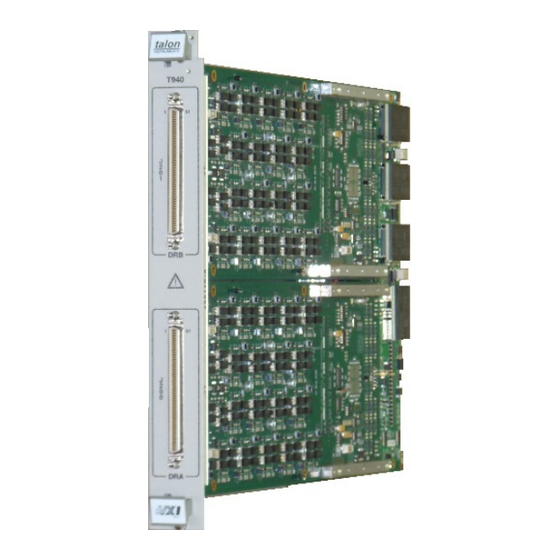
Publication No. 980938 Rev. K Model T940 User Manual Boards (named DRA and DRB for their mounted location). (A T940 module is shown in the photo as an example.) The block diagram in Figure 1-2 shows how the various components work together. -
Page 43: Figure 1-2: Drm Digital Resource Module Block Diagram
Model T940 User Manual Publication No. 980938 Rev. K FRONT POWER DIGITAL BOARD CONVERTER PANEL DRIVER/RECEIVER (OPTIONAL) DATA SEQUENCER BRIDGE INTER DATA MODULE CONTROL SEQUENCER DRIVER/RECEIVER Figure 1-2: DRM Digital Resource Module Block Diagram Front Panel The DRM front panel provides the interface to the device being tested. There is a Driver/Receiver board connector for input and output of signals. -
Page 44: Power Converter (Pc)
Publication No. 980938 Rev. K Model T940 User Manual Power Converter (PC) The PC may be optionally installed on the Digital Board when variable voltage DR boards such as the DR3e, DR9, or UR14 are used. The PC converts backplane voltages into digital bias voltages. Its protection circuitry can detect faults in any of the four on-board power supplies, status of the input fuses, or a high input current or overcurrent condition. -
Page 45: Driver/Receiver Board B (Drb)
Model T940 User Manual Publication No. 980938 Rev. K Driver/Receiver Board B (DRB) The DRB board contains all the driver/receiver logic, relays, sensors and termination circuitry for channels 33 through 64. Model and Part Number Information Model # Description Ordering Part # LVTTL, 32 channels, 100 Ω... - Page 46 Publication No. 980938 Rev. K Model T940 User Manual To create the 2nd, 3rd, and 4th sections of the part # for a configured T940, substitute the [W], “- XXzz,” “-YYzz,” and [-A] in the part # with the correct CIB/Funnel, Application and Power Converter Code from the table below.
-
Page 47: Accessories
Model T940 User Manual Publication No. 980938 Rev. K Accessories Model # Description Ordering Part # Front Panel Signal Flat Ribbon Cable T940/300-XXX 408123-XXX (1 per Driver/Receiver Board) Front Panel Signal Flat Shielded Cable T940/302-XXX 408122-XXX (1 per Driver/Receiver Board) Coaxial Cable, 22 positions, Auxiliary I/O from T940/303-001 408124-001... -
Page 48: Chapter 2
Publication No. 980938 Rev. K Model T940 User Manual Chapter 2 Installation The following sections discuss the installation procedure for the DRM module into a VXI chassis. Before installing the DRM module, ensure that the digital board (DB) DIP switches are set to correct settings for your setup – either in the factory default mode or with specific address and mode settings to your test situation. -
Page 49: Initial Digital Board (Db) Switch Setting
Model T940 User Manual Publication No. 980938 Rev. K Figure 2-2: T940 with Two DR3e Boards Installed Initial Digital Board (DB) Switch Setting WARNING Use standard ESD procedures including ground straps and static-safe work surfaces whenever handling the DRM or any of its Driver/Receiver boards. -
Page 50: Logical Address Selection
Publication No. 980938 Rev. K Model T940 User Manual Do not adjust SW3 VXI Connector VXI Connector Figure 2-3: Digital Board (DB) Switch Locations CAUTION Switch settings shown in Figure 2-2 are for example only and are not particularly what your board should be set to. Refer to the text for proper switch settings. -
Page 51: Vxi Interrupt Selection
Model T940 User Manual Publication No. 980938 Rev. K address. The “ON” setting sets the corresponding bit of the logical address to a one (1). VXI Interrupt Selection The VXI backplane supports 7 levels of interrupts. Using the Slot 0 API functions, interrupt handlers can be installed and enabled for each interrupt level. -
Page 52: Other Settings
Publication No. 980938 Rev. K Model T940 User Manual A32/A24 Register Mapping A32 (factory default) ATTENTION GPIB-VXI slot zero controllers do not support A32 register transfers. A24 register mapping must be selected for DRM operation with these controllers. Other Settings There are a few switch settings that are used for development or debug which, under normal operation, should not be changed. -
Page 53: Bus Request Selection
Model T940 User Manual Publication No. 980938 Rev. K MODE Message Based Enabled VXI Message Based VXI Register Based (Default) Bus Request Selection The VXI backplane supports 4 levels of bus request. Switch positions 2 and 1 of SW2 are used to select the VXI bus request level. Table 2-6: Bus Request Selection Position Signal... -
Page 54: Installing The Module Into A Vxi Chassis
Publication No. 980938 Rev. K Model T940 User Manual Note: Jumper above is shown in the “Terminator” position. Figure 2-4: T940 Inter-Module Mode Jumper Connector Location Terminator Position Secondary Position Primary Position Note: The gray areas in the figure indicate the open portions of the connector. Figure 2-5: T940 Inter-Module Mode Jumper Positions and Settings Installing the Module into a VXI Chassis WARNING... -
Page 55: Figure 2-6: Installing The Drm Into A Chassis
Model T940 User Manual Publication No. 980938 Rev. K ATTENTION Be sure that the VXI chassis has sufficient power and cooling capability – particularly if multiple DR3e, DR4, or DR9 modules are installed into the same chassis. The DRM may be installed in any VXI chassis slot except slot 0 (zero), which is reserved for the Resource Manager. -
Page 56: Figure 2-7: 1263 Series Vxi Chassis (1263Hpf Top, 1263Hpr Bottom)
Publication No. 980938 Rev. K Model T940 User Manual Figure 2-7: 1263 Series VXI Chassis (1263HPf top, 1263HPr bottom) The optional Racal Instruments 1263 High Power 13-slot VXI chassis series (Figure 2-7) is recommended for multiple DRMs which are populated with multiple DR3e, DR4 or DR9 modules. -
Page 57: Initial Power-On
Model T940 User Manual Publication No. 980938 Rev. K Initial Power-On The DRM is normally a register-based VXI module with an embedded processor to manage standard VXI communications. 1. Turn off the chassis power before installing the DRM. 2. Once the DRM is properly installed in a VXI chassis, turn on the chassis power. -
Page 58: Installing The Instrument Driver
Publication No. 980938 Rev. K Model T940 User Manual Included with the instrument driver is the Soft Front Panel (SFP) software. The soft front panel is a graphical user interface for the DRM. It can be used to verify communications and to debug applications during development and integration. The DRM VXIplug&play Instrument Driver uses the VISA communication library to operate the instrument. - Page 59 Model T940 User Manual Publication No. 980938 Rev. K This page was left intentionally blank. Installation 2-12 Astronics Test Systems...
-
Page 60: Chapter 3
Publication No. 980938 Rev. K Model T940 User Manual Chapter 3 DRM Front Panel The DRM front panel provides the hardware interface to the unit under test (UUT). Figures 3-1 and 3-2 illustrate the front panel and its connectors. DRB Channel (J201) T940 shown with two Driver/Receiver boards... -
Page 61: J200 And J201 Dra Channel I/O
Model T940 User Manual Publication No. 980938 Rev. K DRB Channel (J201) DRA/DRB Power and Multi- T940 shown with two Function Signals Driver/Receiver boards on this optional installed (DRA and DRB). connector DRA Channel (J200) Figure 3-2: T940 Front Panel (Showing Optional Front Power Connector) J200 and J201 DRA Channel I/O The J200 and J201 connectors’... -
Page 62: Front Panel Connectors
Publication No. 980938 Rev. K Model T940 User Manual multi-function signals (MFSIG) and grounds to all boards. Figure 3-3: PWR Connector Table 3-1: PWR Connector Pinout Connector Name Connector Name DRB V+ DRB V- DRB MFSIG DRA MFSIG DRA V+ DRA GND DRB GND DRA V-... -
Page 63: Front Panel Lbus Lockout Keys
Model T940 User Manual Publication No. 980938 Rev. K J200/J201 flat ribbon mating cable. 2. DRM cable assemblies are open at one end. Front Panel LBUS Lockout Keys The VXIbus-defined LBUS Lockout Keys are designed to prevent adjacent VXI Modules with incompatible logic families from connecting to the Local Bus. -
Page 64: Lbus Lockout Key Installation
Publication No. 980938 Rev. K Model T940 User Manual Figure 3-5: LBUS Lockout Configuration LBUS Lockout Key Installation In order to accommodate the VXIbus specification’s defined minimum thickness of the lockout key and the clearance provided around the module ejector handle, two LBUS lockout keys must be fitted on top of each other for each module. - Page 65 Model T940 User Manual Publication No. 980938 Rev. K 2. Install two screws in the holes at the top of the module front panel and tighten the screws. 3. Move the ejector handle to the ejected position, and install a third screw in the hole now made accessible.
-
Page 66: Chapter 4
Publication No. 980938 Rev. K Model T940 User Manual Chapter 4 Functional Description This section describes the DRM hardware block diagrams. For information about DRM address maps and register descriptions, contact your local sales representative or contact Sales Support at atsinfo@astronics.com. Digital Board (DB) FRONT CH[1:32]... -
Page 67: Vxi Bridge
Model T940 User Manual Publication No. 980938 Rev. K VXI Bridge TEMPERATURE MONITOR EEPROM VADDR VDATA ADDRESS CONTROL VCTRL SERIAL PROM JTAG ARBITRATION REGISTERS VXI_INT VXI TRIGGERS TTL/ECL Data Sequencer Logic Driver Receiver Logic Figure 4-2: T940 VXI Bridge Block Diagram Terms Used in this Section VADDR (VXI Address Bus) The 32 bit backplane address bus... -
Page 68: Type 1 And Type 3
Publication No. 980938 Rev. K Model T940 User Manual headroom requirements and specifications for each power converter range. Type 1 and Type 3 The type 1 power converter is designed for use in a VXI 3.0 chassis and the type 3 power converter is designed for a VXI 4.0 chassis and utilizes the additional power pins and can supply more current. -
Page 69: Terms Used In This Section
Model T940 User Manual Publication No. 980938 Rev. K LBUSC LBUSA LBUSC LBUSA LBUSC LBUSA LBUSC LBUSA Slot 1 Slot 2 Slot 3 Slot 4 Slot 12 INTER INTER INTER INTER INTER MODULE MODULE MODULE MODULE MODULE CONTROL CONTROL CONTROL CONTROL CONTROL Inter-Module Control... -
Page 70: Description
Publication No. 980938 Rev. K Model T940 User Manual Linked Used to describe two sequencers (DSA and DSB) on the same DRM that are synchronized together. Primary Used to describe the DRM that provides all the timing for the sequencers that are part of the DRS chain. DSA is always coupled to the DRS chain and is the source of the timing and control. - Page 71 Model T940 User Manual Publication No. 980938 Rev. K Primary DRM Inter-Module Modes: These modes apply to a DRM that is jumpered as a Primary. • Independent Not Linked – SIMA set to IMA and SIMB set to IMB. IMJMPR position is a don’t care.
-
Page 72: Examples
Publication No. 980938 Rev. K Model T940 User Manual position is a don’t care. Primary driver disabled. The DRM is not coupled to a DRS. DSA and DSB are not linked. • Independent Linked – SIMA and SIMB set to IMA. IMJMPR position is a don’t care. - Page 73 Model T940 User Manual Publication No. 980938 Rev. K COUPLED DRM5 DRM3 DRM1 DRM6 DRM4 DRM2 LINKED CH 321-384 CH 257-320 CH 193-256 CH 129-192 CH 65-128 CH 1-64 In this example, all 12 sequencers, DSA and DSB on DRM1 through DRM6 are coupled to a single DRS (368 channels).
- Page 74 Publication No. 980938 Rev. K Model T940 User Manual COUPLED DRM5 DRM3 DRM1 DRM6 DRM4 DRM2 LINKED CH 321-384 CH 257-320 CH 193-256 CH 129-192 CH 65-128 CH 1-64 In this example, DSA and DSB on DRM1 and DRM2 are coupled to a DRS (128 channels).
-
Page 75: Data Sequencer
Model T940 User Manual Publication No. 980938 Rev. K COUPLED DRM5 DRM3 DRM1 DRM6 DRM4 DRM2 LINKED CH 321-384 CH 257-320 CH 193-256 CH 129-192 CH 65-128 CH 1-64 In this example, DSA and DSB on DRM1 and DRM2 are coupled to a DRS (128 channels), DSA and DSB on DRM3 and DRM4 are coupled to a second DRS (128 channels), DSA and DSB on DRM5 are linked and running independent of a DRS (64 channels). -
Page 76: Terms Used In This Section
Publication No. 980938 Rev. K Model T940 User Manual Terms Used in this Section 250 MHz 250 MHz clock derived from the 500 MHz clock. 500 MHz 500 MHz oscillator clock. AUX DATA AUX output data value. AUX EN AUX output enable value. AUX I/O AUX output and enable signals as well as the AUX input and probe data. - Page 77 Model T940 User Manual Publication No. 980938 Rev. K Linked Trigger Bus signals connecting DSA to DSB. MCLK Master Clock MPSIG Multipurpose signal output. PAT DEL[1:2] Pattern delay timers. PAT TO Pattern timeout timer. PATADDR Pattern address used by the external pattern RAM. PAUSE Sequence trigger used to stop the timing generator for handshaking applications.
-
Page 78: Sequence Logic
Publication No. 980938 Rev. K Model T940 User Manual Jump 4 Selected Inter-Module signals. START Sequence trigger used to start the pattern controller. STOP Sequence trigger used to stop the pattern controller. SYNC[1:2] Programmable sync pulse signals. TEST CODE Selects the jump test event. T0 CLK Internal SEQ CLK generated by the sequence controller. -
Page 79: System Clock
Model T940 User Manual Publication No. 980938 Rev. K System Clock This block selects the sequence clock signal used by the sequence controller. Test Logic This block determines if a valid conditional jump is enabled or not. Record Control This block generates the address for the Record RAM based on the Recording Mode. -
Page 80: Pattern Ram
Publication No. 980938 Rev. K Model T940 User Manual Pattern RAM The output code as well as the input code for every channel of each pattern is stored in the Pattern RAM. Record RAM This is where the individual channel results are stored. The channel results are either the pattern input compare result or raw response data based on RH or RL. -
Page 81: Driver/Receiver
Model T940 User Manual Publication No. 980938 Rev. K Driver/Receiver The DRM can accommodate two Driver/Receiver boards (named DRA or DRB for their mounted location). Each Driver/Receiver board contains unique driver/receiver circuitry and front panel connector pinouts that are described in an appendix dedicated to each specific Driver/Receiver type. -
Page 82: Chapter 5
Publication No. 980938 Rev. K Model T940 User Manual Chapter 5 Soft Front Panel Operation The Soft Front Panel (SFP) is a stand-alone executable that can be used to program, query and run the DRM digital resource. Regardless of the user’s choice of programming path (VXIplug&play instrument driver, A24/A32 register-based access, or a combination of these) the following basic 7-step process is required to implement a DRM test program: 1. -
Page 83: Sfp Main Panel
Model T940 User Manual Publication No. 980938 Rev. K When started, the SFP searches for all the installed DRMs in the VXI system. If more than one DRM is detected, a dialog box prompts the user to select the DRM to initialize. Each instance of the SFP opens a VXI session with a single DRM in the system. -
Page 84: Figure 5-3: Main Panel
Publication No. 980938 Rev. K Model T940 User Manual Title Menu Company Chassis Logo Data Active Module Module Data Data Figure 5-3: Main Panel Figure 5-4: Main Panel UR14 Astronics Test Systems Soft Front Panel Operation 5-3... -
Page 85: Company Logo
Model T940 User Manual Publication No. 980938 Rev. K The following sections describe the main panel controls and indicators. Company Logo Pressing this control displays the information panel. Figure 5-5: Company Information Panel Active LED The Active LED indicates whether a VXI session has been established successfully. -
Page 86: Sfp Main Panel Menu Bar
Publication No. 980938 Rev. K Model T940 User Manual SFP Main Panel Menu Bar The SFP main panel menu bar provides access to select, program and save the DRM hardware. Relevant VXIplug&play API functions are included with the menu options. Figure 5-6: Menu Bar File Menu Figure 5-7: File Menu... -
Page 87: Config Menu
Model T940 User Manual Publication No. 980938 Rev. K Menu Option Description and inserted in the history list [tat964_loadConfiguration] Save Updates the configuration file with the latest editing changes [tat964_saveConfiguration] Save As Creates a new configuration file with the latest editing changes. -
Page 88: Edit Menu
Publication No. 980938 Rev. K Model T940 User Manual AUX Outputs Displays the panel for programming auxiliary output parameters Interrupts Displays the panel for programming the interrupt parameters Edit Menu The Edit Menu is used to create, program and modify timing sets, pattern sets and sequences. -
Page 89: Instrument Menu
Model T940 User Manual Publication No. 980938 Rev. K Instrument Menu The Instrument Menu is used to run self-test, calibration and monitor routines on the DRM hardware. Figure 5-11: Instrument Menu Table 5-5: Instrument Menu Descriptions Menu Option Description Self-Test Runs the self-test Full RAM Test Runs the full RAM test... -
Page 90: Opening A Vxi Drm Session
Publication No. 980938 Rev. K Model T940 User Manual Table 5-6: Help Menu Descriptions Menu Option Description Contents Displays the VXIPNP API help file table of contents About DRM Displays revision data for the DRM Soft Front Panel executable Figure 5-13: About DRM Driver Screen Opening a VXI DRM Session Starting the SFP initiates a search for all DRMs using the VISA library. -
Page 91: Configuring The Global Hardware Parameters
Model T940 User Manual Publication No. 980938 Rev. K Figure 5-14: Opening a VXI DRM Session Relevant VXIplug&play API functions include: • tat964_init • tat964_autoConnectToAll • tat964_autoConnectToFirst • tat964_autoConnectToLA • tat964_autoConnectToSlot Configuring the Global Hardware Parameters Configuring the global hardware parameters is done from three panels: Configure Module, Configure Data Sequencer A, and Configure Data Sequencer B. -
Page 92: Inter-Module Mode
Publication No. 980938 Rev. K Model T940 User Manual Figure 5-15: Configure Module Panel The following sections describe the Configure Module panel controls. Inter-Module Mode This pull-down control programs the control source for the DSA and DSB sequencers. The T940 chain and termination are set via jumpers. If a jumper is not installed, the DRM can only be configured as Independent Not Linked or Independent Linked. -
Page 93: Table 5-8: Inter-Module Mode Settings
Model T940 User Manual Publication No. 980938 Rev. K DRM Type Description Primary The Primary module must be located in the rightmost slot position in the VXI chassis relative to the DRM modules that will be coupled. DSA provides all the timing for the sequencers that are part of the coupled chain . -
Page 94: Power Converter
Publication No. 980938 Rev. K Model T940 User Manual Setting DSA Control DSB Control DRM Type Secondary DSB Coupled Secondary Secondary DSA and DSB Secondary Coupled Terminator Not Linked Terminator Terminator Linked Terminator Terminator DSA Coupled Terminator Terminator DSB Coupled Terminator Terminator DSA and DSB Terminator... -
Page 95: Ltbn Signal
Model T940 User Manual Publication No. 980938 Rev. K Figure 5-16: Configure Linked Trigger Bus Panel LTBn Signal This pull-down control programs the signal source for the specified LTB trigger. The selections for this pull-down control are: Table 5-10: LTB Signal Pull-Down Settings Setting Description None... -
Page 96: Invert
Publication No. 980938 Rev. K Model T940 User Manual The relevant VXIplug&play API function is: • tat964_setLtbTriggers Invert This Invert button is used to invert the associated signal. The relevant VXIplug&play API function is: • tat964_setLtbTriggers Direction The direction pull-down sets the signal direction. Table 5-11: Direction Settings Setting Description... -
Page 97: Offset
Model T940 User Manual Publication No. 980938 Rev. K Offset The group offset specifies the operating voltage window of the group channels. The selections for this pull-down control are: Table 5-12: Group Offset Attribute Settings Setting Description Zero HV -15.5V to 15.5V 0V to +31V -31V to 0V Verify that the Min and Max settings are within the window before updating. -
Page 98: Oc Src
Publication No. 980938 Rev. K Model T940 User Manual Table 5-13: Group Slew Attribute Settings Setting Description Fast Fast recommended for low voltage swings and fast data rates. Medium Slow Slow Default Low recommended for high voltage swings and low data rates. The slew attribute is updated immediately when changed. -
Page 99: Group [1
Model T940 User Manual Publication No. 980938 Rev. K Group [1..3] These toggle buttons turn the group state on or off. The relevant VXIplug&play API function is: • tat964_setGroupState Delay Signal The DRM uses the VXI local bus signal to function in a multi-module operation. During the alignment process, the local bus signals need to be delayed in order to align the timing skew between modules. -
Page 100: Ttltrg And Ecltrg Signal
Publication No. 980938 Rev. K Model T940 User Manual Figure 5-18: Set VXI Triggers DSA Panel The TTLTRG lines are open collector on the VXI backplane. The chassis provides a split termination which provides a weak pull-up (thus there is a slow rising edge recovery time). -
Page 101: Invert
Model T940 User Manual Publication No. 980938 Rev. K Setting Description of the VXI Trigger Source Signal AUX1-AUX12 Selects the specified AUX input signal from the front panel Halted Used for DRS halt operation between coupled sequencers Probe Button Selects the state of the probe button Pulse Generator Selects the pulse generator signal Sequence Flag 1-2... -
Page 102: Dut_Gnd
Publication No. 980938 Rev. K Model T940 User Manual Figure 5-19: Configure DSn D/R Properties Panel DUT_GND For the DR3e/DR4/DR9/UR14, this control is used to program a relay that will connect the DUT_GND reference for the Pin Electronics to either a front panel DUT_GND or to signal ground. -
Page 103: Mfsig Source
Model T940 User Manual Publication No. 980938 Rev. K The relevant VXIplug&play API function is: • tat964_setVoltageRangeMode Note: This function is inoperable for the DR1, DR2, DR4, DR7, and DR8. MFSIG Source This pull-down control programs the power connector MFSIG signal function. The DR3e Driver/Receiver boards have an optional front panel power connector that is used to provide the V+/V- rail voltages to the Pin Electronics devices. -
Page 104: Error Pulse Width
Publication No. 980938 Rev. K Model T940 User Manual The relevant VXIplug&play API function is: • tat964_setMpsigSource Error Pulse Width This pull-down programs the error signal pulse width. The error pulse is a DRS signal used for counting and recording errors. The error pulse width is set during the DRS timing bus calibration with the Rev J driver or later and sequencer revision 0.20 or later. -
Page 105: Config Data Sequencer A/B
Model T940 User Manual Publication No. 980938 Rev. K Table 5-20: Record Mode Settings Setting Description Typical Usage Disabled The contents of the record memory will not Setting Record Mode to Disabled change during the next burst if Step Record insures that the record memory will not Mode is set to either None or Record be written to when Step Record Mode is... -
Page 106: Master Clock
Publication No. 980938 Rev. K Model T940 User Manual Figure 5-21: Configure Clocks Master Clock This pull-down control programs the sequencer master clock source. The master clock defines the sequencer timing resolution. The resolution is half of the master clock period. The selections for this pull-down control are: Table 5-21: Master Clock Source Settings Setting... -
Page 107: System Clock
Model T940 User Manual Publication No. 980938 Rev. K System Clock This pull-down control programs the sequencer System Clock source. The System Clock signal defines the pattern period. The selections for this pull-down control are: Table 5-22: System Clock Source Settings Setting Description Typical Usage... -
Page 108: External Offset
Publication No. 980938 Rev. K Model T940 User Manual The relevant VXIplug&play API function is: • tat964_setSystemClockParameters External Offset This control is used to specify the external System Clock offset in order to align the clock/data relationship. The valid offset range is from 0 to 65534 (even numbers only) and the resolution is 1/2 the MCLK period. -
Page 109: Configure Timers
Model T940 User Manual Publication No. 980938 Rev. K Configure Timers Access this panel from the menu bar: Config > Data Sequencer x> Timers. (Where “x” is the sequencer you wish to configure.). The DRM has five timers: • Watchdog •... -
Page 110: Watchdog Action
Publication No. 980938 Rev. K Model T940 User Manual • The timer is reset at the beginning of every step unless the sequence timeout continue flag is set in the Edit Sequence Step panel. • Cannot be nested. • Does not stop during a Pause or Halt (including single-stepping). •... -
Page 111: Watchdog Time
Model T940 User Manual Publication No. 980938 Rev. K • tat964_setWatchdogTimer Watchdog Time This numeric control is used to specify the watchdog timeout count. The timeout is programmed in 20 ns steps with a range of 40 ns to 4000 s. The watchdog timer set resolution adjusts based on the timeout value: Table 5-26: Watchdog Timer Resolution Ranges Timer Setting... -
Page 112: Pattern Delay 1-2
Publication No. 980938 Rev. K Model T940 User Manual • tat964_setPatternTimer Pattern Delay 1-2 This numeric control is used to specify the pattern delay. The pattern delay is programmed in 10 ns steps with a range of 20 ns to 42.949672970 s. -
Page 113: Trigger
Model T940 User Manual Publication No. 980938 Rev. K Execute Start Trigger The execute start trigger causes the selected sequence step to start. Selecting a sequence step consists of arming the sequence step. In a linked or DRS configuration, all of the coupled sequencers need to be armed first. -
Page 114: Test Condition
Publication No. 980938 Rev. K Model T940 User Manual The selections for this pull-down control are: Table 5-29: Trigger Source Settings Setting Description None No trigger source selected AUX1-AUX12 Trigger source set to front panel signal CHT1 Trigger source set to channel test 1 ECLTRG0,1 Trigger source set to VXI ECL trigger... -
Page 115: Input Mode
Model T940 User Manual Publication No. 980938 Rev. K • tat964_setPhaseResumeTrigger • tat964_setJumpTrigger • tat964_setHaltTrigger • tat964_setExecuteStartTrigger • tat964_setExecuteStopTrigger Input Mode This pull-down control programs the trigger input mode. The selections for this pull-down control are: Table 5-31: Trigger Input Mode Settings Setting Description Normal... -
Page 116: Configure Pulse Generator
Publication No. 980938 Rev. K Model T940 User Manual The relevant VXIplug&play API functions are: • tat964_setPauseTriggerReset • tat964_setHaltTriggerReset • tat964_setJumpTriggerReset Configure Pulse Generator Access this panel from the menu bar: Config > Data Sequencer x> Pulse Generator (where “x” is the sequencer you wish to configure). Figure 5-24: Configure Pulse Generator Each data sequencer has a programmable pulse generator that can be routed to the following signals:... -
Page 117: Step
Model T940 User Manual Publication No. 980938 Rev. K The selections for this pull-down control are: Table 5-33: Pulse Generator Mode Settings Setting Description Continuous The pulse generator begins continuous output when armed Continuous Start The pulse generator begins continuous output from the start of the sequence when armed Single Start The pulse generator outputs a single pulse... -
Page 118: Width
Publication No. 980938 Rev. K Model T940 User Manual If the resolution is 10 ns, the delay is programmed in 10 ns steps with a range of 20 ns to 42.949672970 s (with an uncertainty of ±5 ns). If the resolution is 20 ns, the delay is programmed in 20 ns steps with a range of 20 ns to 85.899345920 s (with an uncertainty of ±5 ns). -
Page 119: Error Record Basis
Model T940 User Manual Publication No. 980938 Rev. K Figure 5-25: Data Sequencer Configure Settings Panel Error Record Basis This pull-down control programs the sequencer error record basis. This control allows the user to select how the response data will be evaluated for errors when the record mode is set to Record Errors. -
Page 120: Record Type
Publication No. 980938 Rev. K Model T940 User Manual delay. See the Record Offset section in Chapter 8 for more details about using this feature. The valid offset range is from 0 to 63 MCLKs. The relevant VXIplug&play API function is: •... -
Page 121: Error Address Basis
Model T940 User Manual Publication No. 980938 Rev. K Counting and Logging Errors section in Chapter 8 including data rate limitations. The relevant VXIplug&play API function is: • tat964_setErrorParameters Error Address Basis This pull-down control programs the sequencer error address basis. This control allows the user to select which error signal causes an error to be recorded in the Error Address Memory. -
Page 122: Output-To-Input Disable
Publication No. 980938 Rev. K Model T940 User Manual Indexed 4096 sequence steps with 256 timing sets indexed. Four phase/window signals per timing set. The relevant VXIplug&play API function is: • tat964_setTimingMode Output-to-Input Disable This pull-down control programs the output-to-input disable setting. When a channel transitions from an output pattern code to an input pattern code, this enable can be set to disable the output at the beginning of the pattern (System Clock) or on a phase assert. -
Page 123: Pass Valid Mode
Model T940 User Manual Publication No. 980938 Rev. K Chapter 8. The relevant VXIplug&play API function is: • tat964_setPassFailParameters Pass Valid Mode This pull-down control programs the sequencer pass valid mode. This control allows the user to define the Pass as a Valid Pass. A Valid Pass is one where no channel errors were detected but there must be at least one valid pattern expect code for each pattern in the sequence step. -
Page 124: Over-Current
Publication No. 980938 Rev. K Model T940 User Manual Over-Current This command button displays the Over-Current panel so the over-current parameters can be programmed for the selected sequencer. The over-current mode should be used for channels configured in the static mode only. -
Page 125: Drive Fault
Model T940 User Manual Publication No. 980938 Rev. K Table 5-43: Over-Current Window Settings Setting Description 4’ – 8’ Set window to cables between 4 and 8 feet 8.3’ – 16.3’ Set window to cables between 8.3 and 16.3 feet 16.6’... -
Page 126: Probe
Publication No. 980938 Rev. K Model T940 User Manual pattern codes and can be used to detect dynamic over-current conditions. If enabled a drive fault will disable all channels of the specified sequencer and a drive fault event will be generated. Use tat964_querySequencerEvent() to query the drive fault event and tat964_querySequencerDriveFault() to query which channel caused the drive fault. -
Page 127: Offset
Model T940 User Manual Publication No. 980938 Rev. K Counting and Logging Errors section of Chapter 8 for a discussion on the impact of the Probe State on data rates. The relevant VXIplug&play API function is: • tat964_setProbeInterfaceState Offset The Probe offset allows the user to shift the probe record signals to accommodate system and UUT delay. -
Page 128: Probe Button
Publication No. 980938 Rev. K Model T940 User Manual Setting Description Window 4 Window 4 open edge samples the Open CRC. Window 4 Window 4 close edge samples the Close CRC. The relevant VXIplug&play API function is: • tat964_setProbeConfiguration Probe Button This control sets the probe button action. -
Page 129: Probe Cal Connect
Model T940 User Manual Publication No. 980938 Rev. K probe input is routed through AUX1 A on the UR14 Driver/Receiver board. The relevant VXIplug&play API function is: • tat964_setProbeLevels Probe Cal Connect This control opens and closes the probe calibration channel connect relay. The probe calibration is routed through AUX2 A on the UR14 Driver/Receiver board. -
Page 130: Dc Cal
Publication No. 980938 Rev. K Model T940 User Manual The user is then prompted to adjust the probe compensation screw until the probe module LED labeled D1 illuminates. The relevant VXIplug&play API function is: • tat964_probeCalibration DC Cal This control initiates a DC level calibration. The user is prompted to connect the probe to the calibration BNC. -
Page 131: Attributes
Model T940 User Manual Publication No. 980938 Rev. K • tat964_probeCalibration Attributes This command button on the Configure DSA Settings panel displays the Attribute panel so that the sequencer attributes can be programmed. Figure 5-28: Attribute Panel Jump Pass Fail This control sets the sequencer step pass/fail accumulator mode. -
Page 132: Window 3 Mode
Publication No. 980938 Rev. K Model T940 User Manual Table 5-50: Phase 3 Mode Settings Setting Description Typical Usage Normal Phase 3 is sourced from the internal Internally programmed timing for drive phase generator. (Default) phases. Jump 1 Phase 3 is sourced form the Jump 1 Externally programmed timing controlled by an external stimulus clock trigger signal. -
Page 133: Crc Algorithm And Capture Mask
Model T940 User Manual Publication No. 980938 Rev. K The selections for this pull-down control are: Table 5-52: CRC Preload Settings Setting Description Zeros Preload 0’s Ones Preload 1’s Masked Mask Preload The relevant VXIplug&play API function is: • tat964_setSequencerAttribute CRC Algorithm and Capture Mask These numeric controls set the number for the CRC algorithm and for the CRC capture mask settings and are available in sequencer revision 0.23 and later. -
Page 134: Configuring The I/O Channels
Publication No. 980938 Rev. K Model T940 User Manual Table 5-54: Static State Settings Setting Description Disable static operation Enable static operation. The relevant VXIplug&play API function is: • tat964_setStaticState Configuring the I/O Channels Configuring the channels is a three step process: 1. -
Page 135: Channel Parameters
Model T940 User Manual Publication No. 980938 Rev. K 1. Left click on the desired channel in the channel list control. A check mark indicates the channel has been selected. Multiple channels can be selected. 2. Use the pull down list box to select the desired channels and press the Select command button. -
Page 136: Stimulus Format
Publication No. 980938 Rev. K Model T940 User Manual The relevant VXIplug&play API function is: • tat964_setChannelParameters Stimulus Format This pull-down control programs the stimulus data formatting for the selected channel(s). The selections for this pull-down control are: Table 5-56: Stimulus Format Settings Setting Stimulus Format Description •... -
Page 137: Capture Signal
Model T940 User Manual Publication No. 980938 Rev. K Setting Stimulus Format Description • Comp Surround Start of Pattern – Output driver goes to complemented level determined by the Pattern Code instruction in Pattern Memory • Phase Assert – Output driver goes to level determined by the Pattern Code instruction in Pattern Memory. -
Page 138: Capture Mode
Publication No. 980938 Rev. K Model T940 User Manual Table 5-57: Capture Signal Settings Setting Description Window 1 Use Window 1 timing signal to control input comparator timing. Window 2 Use Window 2 timing signal to control input comparator timing. Window 3 Use Window 3 timing signal to control input comparator timing. -
Page 139: Properties
Model T940 User Manual Publication No. 980938 Rev. K Table 5-59: Static Mode Settings Setting Description Static Mode enabled for selected channel(s). Static mode disabled for selected channel(s. Note: The static state must be enabled before setting the static mode. The relevant VXIplug&play API function is: •... -
Page 140: Driver Levels
Publication No. 980938 Rev. K Model T940 User Manual Figure 5-30: Configure Channel Properties Panel Driver Levels The driver levels allow the user to set the Drive High (DVH) and Drive Low (DVL) voltage. The min/max levels are dependent on the installed Driver/Receiver board as well as the voltage mode. -
Page 141: Comparator Levels
Model T940 User Manual Publication No. 980938 Rev. K • tat964_setChannelSourceLevels Comparator Levels The comparator levels allow the user to set the Compare High (CVH) and Compare Low (CVL) voltage. The min/max levels are dependent on the installed Driver/Receiver board as well as the voltage mode. -
Page 142: Over-Current Alarm Levels
Publication No. 980938 Rev. K Model T940 User Manual Over-Current Alarm Levels This allows the user to set the over-current high (OC High (mA)) and over- current low (OC Low (mA)) alarm levels for static current limits on the DR3e, DR9, and UR14 (see Drive Fault for dynamic current limiting). -
Page 143: Figure 5-31: Current Load
Model T940 User Manual Publication No. 980938 Rev. K Source VCOM Low Load State VCOM High Sink Figure 5-31: Current Load When the channel voltage is greater than the VCOM High level, the Sink current becomes active. When the channel voltage is less than the VCOM Low level, the Source current becomes active. -
Page 144: Channel Connect
Publication No. 980938 Rev. K Model T940 User Manual The relevant VXIplug&play API functions are: • tat964_setChannelSenseParameters • tat964_setChannelLoadState Channel Connect This control allows the user to control the isolation and analog bypass relays. The selections for this pull-down control are: Table 5-63: Channel Connect Settings Setting Description... -
Page 145: Channel Mode
Model T940 User Manual Publication No. 980938 Rev. K The relevant VXIplug&play API function is: • tat964_setComparatorDelay Channel Mode This control programs the front panel channel mode setting. The channel mode can be set to: • Single-ended • Differential with 100 Ω differential termination •... -
Page 146: Compare Input (V)
Publication No. 980938 Rev. K Model T940 User Manual Figure 5-33: Configure UR14 Channel Properties Panel Compare Input (V) This control sets the comparator level of the selected channel group. Min: 0.0 Max: 20.0 The relevant VXIplug&play API function is: •... -
Page 147: Figure 5-34: Configure Aux Channels Panel
Model T940 User Manual Publication No. 980938 Rev. K Figure 5-34: Configure AUX Channels Panel Figure 5-35: Configure AUX Channels Panel UR14 The AUX channels are a set of 12 multi-purpose signals that can be used for any of the following I/O resources: 1. -
Page 148: Table 5-64: Drn Aux Configuration
Publication No. 980938 Rev. K Model T940 User Manual 4. Vector Jump Address Input 5. Waveform Output 6. Pulse Generator Output 7. Sync Output 8. Frequency Synthesizer Output 9. Timing Set Output Signals a. Phase b. Window c. T0_CLK d. Pattern Clock 10. -
Page 149: Configuring The Aux/Uaux Signals
Model T940 User Manual Publication No. 980938 Rev. K Signal Logic Special Use AUX6 A LVTTL Shares front panel pin with AUX10 A AUX7 A LVTTL Shares front panel pin with AUX11 A AUX8 A LVTTL Shares front panel pin with AUX12 A AUX9 A ECL differential or bipolar... -
Page 150: State
Publication No. 980938 Rev. K Model T940 User Manual State This control allows the user to set the output state for the selected AUX signal. Table 5-66: AUX Output State Settings Setting Description Disable the AUX output. Enable the AUX output. Enable and invert the AUX output. -
Page 151: Input Bus Source
Model T940 User Manual Publication No. 980938 Rev. K Setting Description FS Reference Frequency synthesizer reference signal Frequency Synthesizer Frequency synthesizer signal Jump Strobe Test signal Int Error Test signal Ext Error Test signal HIGH Drive high PASS PASS flag FAIL FAIL flag CONDEN... -
Page 152: Connect State
Publication No. 980938 Rev. K Model T940 User Manual Setting Description ECLTRG0,1 Source set to VXI ECL trigger TTLTRG0-7 Source set to VXI TTL trigger LTB0-7 Source set to Linked Trigger bus signal Connect State This control allows the user to open or close the isolation relay. DR2 and DR7 Driver/Receiver boards do not have isolation relays. -
Page 153: Configuring The Interrupts
Model T940 User Manual Publication No. 980938 Rev. K Table 5-70: Logic Mode Settings Setting Description LVTTL AUX configured as LVTTL. ECL Bipolar ECL AUX configured as differential ECL The relevant VXIplug&play API function is: • tat964_setAuxLogicMode Configuring the Interrupts There are five hardware groups on the T940 that are capable of generating VXI interrupt. -
Page 154: Condition
Publication No. 980938 Rev. K Model T940 User Manual Figure 5-37: Configure Interrupt Condition This control indicates that the interrupt condition is currently true. The relevant VXIplug&play API function is: • tat964_queryInterruptCondition Event True This control enables a VXI interrupt to be generated when any of the associated hardware groups enabled event bits goes from false to true. -
Page 155: Editing The Data Sequencers
Model T940 User Manual Publication No. 980938 Rev. K Editing the Data Sequencers Editing the data sequencers consists of programming the following: 1. Timing Sets 2. Patterns 3. Waveforms 4. Sequence Parameters 5. Sequence Steps Figure 5-38: Editing the Data Sequencers Editing the Timing Sets The timing sets are used to control the channel drivers and receivers. -
Page 156: Figure 5-40: Data Sequencer Timing Sets Panel
Publication No. 980938 Rev. K Model T940 User Manual The figure above represents two channels with the following configuration: • Output Signal = Phase 1 Stimulus Format = Return to One Pattern Code = Drive Low • Output Signal = Phase 2 Stimulus Format = Non Return Pattern Code = Drive High The Assert signal (rising edge) causes the pattern code to be loaded. -
Page 157: Timing Set Value Rules
Model T940 User Manual Publication No. 980938 Rev. K • Indexed – 256 timing sets with four phase/window groups per timing set and 4096 sequence steps where each sequence step points to one of the 256 timing sets. Double-click on one of the available Assert/Return/Open/Close cells. Enter the desired value using the numeric keys or the up/down arrows followed by the Enter key. -
Page 158: Phase/Window Spanning
Publication No. 980938 Rev. K Model T940 User Manual 2. Idle/Standby Timing Phase/Window Spanning Phase/Window spanning allows the user to Assert/Open the timing signal in one pattern and Return/Close the signal in a different pattern. The following steps describe how to span timing signals across multiple patterns: 1. -
Page 159: Append
Model T940 User Manual Publication No. 980938 Rev. K Figure 5-41: Edit Patterns Panel This panel lists all the defined pattern sets. The associated step number, size and offset are displayed. The size of a pattern set can be from 1 to 262144. The offset can be from 0 to 262140 and must be a multiple of four. -
Page 160: Assign
Publication No. 980938 Rev. K Model T940 User Manual Figure 5-42: Append Data Sequencer Pattern Sets Panel Enter the Number of Patterns to append and press the Apply command button. Append pattern memory will be initialized to Pattern Code “R”, which repeats the previous code. -
Page 161: Edit Data
Model T940 User Manual Publication No. 980938 Rev. K Figure 5-43: Assign Data Sequencer Pattern Sets Panel Enter the new Size and/or Offset and press the Apply command button. Assigned pattern memory will not be initialized. Press the Close command button to exit the panel without any changes. The relevant VXIplug&play API function is: •... -
Page 162: Figure 5-44: Pattern Set Sequencer Data Panel
Publication No. 980938 Rev. K Model T940 User Manual Figure 5-44: Pattern Set Sequencer Data Panel Each column contains the TEST code, PROBE code and the pattern codes for all the channels. The pattern codes are described in Figure 5-47 and Table 5-TTT. The pattern set is displayed in pages of 32 patterns. -
Page 163: Figure 5-46: Goto Pattern Panel
Model T940 User Manual Publication No. 980938 Rev. K To jump to a specific pattern number, right click in any of the cells to display the Goto Pattern panel Figure 5-46: Goto Pattern Panel The menu bar: View > Pattern Codes displays a legend of all the available TEST and CH entries. -
Page 164: Figure 5-48: Probe Codes
Publication No. 980938 Rev. K Model T940 User Manual The row labeled “PROBE” displays the probe expect code for each pattern. There are thirty four probe expect codes: Figure 5-48: Probe Codes Astronics Test Systems Soft Front Panel Operation 5-83... -
Page 165: Table 5-71: Probe Expect Codes
Model T940 User Manual Publication No. 980938 Rev. K Table 5-71: Probe Expect Codes Expect Probe Code Shortcut Description Code Signal starts above RH and crosses the RH and RL once and ends below RL. Signal starts above RH, crosses RH once, crosses RL three or more times and ends below RL. - Page 166 Publication No. 980938 Rev. K Model T940 User Manual Expect Probe Code Shortcut Description Code three or more times, crosses RH once and ends above RH. Signal remains between RL and RH Signal starts between RL and RH, crosses the RH once and ends above RH. Signal starts between RL and RH, crosses the RL once and ends below RL.
-
Page 167: Figure 5-49: Pattern Set Data - File Menu
Model T940 User Manual Publication No. 980938 Rev. K pattern code affects the driver/comparator. Table 5-72: Pattern Codes Pattern Code Driver Comparator Invert Code Expect Mode Level Disable Channel ‘Z’ None Disable Channel ‘Z’ Collect CRC ‘C’ Enable CRC Collect CRC ‘C’ Drive High ‘1’... -
Page 168: Import/Export File Format
Publication No. 980938 Rev. K Model T940 User Manual • Pattern data as ASCII Hex • Pattern data as ASCII String • Pattern data as Binary • Pattern data and flags as ASCII Hex • Pattern data and flags as ASCII String •... -
Page 169: Table 5-73: Ascii/Binary Data Format
Model T940 User Manual Publication No. 980938 Rev. K Table 5-73: ASCII/Binary Data Format Pattern Code ASCII/Binary Value ‘Z’ ‘C’ ‘0’ ‘1’ ‘R’ ‘I’ ‘L’ ‘H’ ‘V’ ‘B’ ‘l’ ‘h’ ‘/’ ‘\’ Flag Code Bit15, Bit 14 Code ‘a’ ‘b’ ‘c’... -
Page 170: Binary
Publication No. 980938 Rev. K Model T940 User Manual Probe Expect Bit 13 through Bit ‘7’ ‘8’ The ASCII characters are in four groups of eight characters and one line per pattern. A fifth column of four characters is present if flags and probe expect is included. -
Page 171: Ascii String
Model T940 User Manual Publication No. 980938 Rev. K ASCII String The ASCII string format represents pattern data as viewable ASCII strings, one character per channel, 32 characters per line (34 if flag and probe data are included). Each character is one of the pattern codes listed in Table 5-44. - Page 172 Publication No. 980938 Rev. K Model T940 User Manual (Where “x” is the sequencer you wish to configure.) Figure 5-50: Edit Waveforms Panel Waveform 1 Figure 5-51: Edit Waveforms Panel Waveform 5 Table Size This pull-down control programs the waveform table size for waveforms 1-4. Astronics Test Systems Soft Front Panel Operation 5-91...
-
Page 173: Waveform
Model T940 User Manual Publication No. 980938 Rev. K Waveforms 5 and 6 are fixed at 65536. The selections for this pull-down control are: Table 5-75: Waveform Table Size Settings Setting Description 16 x 1K 16 tables each with 1024 bits 8 x 2K 8 tables each with 2048 bits 4 x 4K... -
Page 174: Editing Sequence Parameters
Publication No. 980938 Rev. K Model T940 User Manual No transitions; Would generate the following waveform; "111..." Bits 1 through the size of the table high. Waveform five and six have a maximum of two transitions. The relevant VXIplug&play API function is: •... -
Page 175: Pipeline
Model T940 User Manual Publication No. 980938 Rev. K Given the following sample loop sequence: Step 1 jump step 1 using LC0 count 2 Step 2 jump step 1 using LC1 count 3 Example 1: If both loop counters reload on terminal count, then the step order will be: 1, 1, 2, 1, 1, 2, 1, 1, 2, 1, 1, 2 Example 2: If loop counter 0 is set to disable, then the step order will be:... -
Page 176: Set Vector Bits
Publication No. 980938 Rev. K Model T940 User Manual Window 4 Sets the closing edge of window 4 as the vector strobe. The relevant VXIplug&play API function is: • tat964_setVectorJumpStrobe Set Vector Bits This command button displays the Edit Vector Bits panel so the vector bit signal selection can be programmed for the selected sequencer. -
Page 177: Input Mode
Model T940 User Manual Publication No. 980938 Rev. K Table 5-77: Vector Bit Source Settings Setting Description None No trigger source selected AUX1-AUX12 Trigger source set to front panel signal CHT1 Trigger source set to channel test 1 ECLTRG0,1 Trigger source set to VXI ECL trigger TTLTRG0-7 Trigger source set to VXI TTL trigger... -
Page 178: Vector Bit Index
Publication No. 980938 Rev. K Model T940 User Manual Figure 5-54: Edit Vector Table Panel Vector Bit Index This allows the user to enter the index to program. There are 16 indexes that can be set (0 to 15). The index is the binary value of the vector bits (VA0 through VA3). -
Page 179: Expect
Model T940 User Manual Publication No. 980938 Rev. K bus. In addition channel test 1 result can also be routed to any of the sequence triggers. Figure 5-55: Sequencer Channel Test Panel Expect This allows the user to enter the expect value for the channel test signal. Bit 0 of the expect value maps to the lowest channel of this sequencer and Bit 31 maps to the highest channel and this is the case for both A and B sequencers. -
Page 180: Editing Sequence Steps
Publication No. 980938 Rev. K Model T940 User Manual Editing Sequence Steps The sequence steps are used to control the flow of the patterns and assign timing. Access this panel from the menu bar: Edit > Data Sequencer x> Sequence Steps. -
Page 181: Internal T0Clk
Model T940 User Manual Publication No. 980938 Rev. K Figure 5-57: Sequence Step Data Panel Internal T0CLK This control allows the user to specify the Internal T0CLK period. When the system clock source is set to internal T0CLK, this control specifies the system clock period. -
Page 182: Cpp Phase And Window Triggering
Publication No. 980938 Rev. K Model T940 User Manual Example 1: CPP = 1 System Clock Pattern Clock Period = Sytem Clock Example 2: CPP = 2 System Clock Pattern Clock Period = 2 x Sytem Clock Example 3: CPP = 3 System Clock Pattern Clock Period = 3 x Sytem Clock... -
Page 183: Last Step
Model T940 User Manual Publication No. 980938 Rev. K Last Step This control allows the user to specify the Last Step flag. This flag indicates whether the current step is the last step of the sequence burst (True) or a sub- step of a multi-step burst (False). -
Page 184: Jump Step
Publication No. 980938 Rev. K Model T940 User Manual Gosub to step 10 and step 13 has the Gosub Return flag set, then the step number sequence starting from 1 would be, 1, 2, 3, 4, 5, 10, 11, 12, 13, 6, 7, 10, 11, 12, 13, 8, 9 … The selections for this pull-down control are: Table 5-81: Jump Type Settings Setting... -
Page 185: Loop Count
Model T940 User Manual Publication No. 980938 Rev. K Setting Description Step FAIL Jump if the PASS/FAIL flag is equal to FAIL Step PASS Jump if the PASS/FAIL flag is equal to PASS Sequence FAIL Jump if Burst Error Count is not equal to zero. Sequence PASS Jump if Burst Error Count is equal to zero. -
Page 186: Loop Counter
Publication No. 980938 Rev. K Model T940 User Manual Loop Counter This numeric control programs the Loop Counter number. Jumps can be qualified by a loop counter. Sixteen loop counters are available. Nested loops are supported including up to all 16 counters. The relevant VXIplug&play API function is: •... -
Page 187: Timing
Model T940 User Manual Publication No. 980938 Rev. K burst: 1. Error Address Memory 2. Record Index Memory 3. Record Memory There is also the Error Counter which counts the number of pattern errors that occurred during the previous sequence burst. The Error Count can be queried using the "tat964_queryErrorFlags"... -
Page 188: Patterns
Publication No. 980938 Rev. K Model T940 User Manual Editing the Timing Sets in Chapter 5). Figure 5-58: Edit Timing Set Panel The relevant VXIplug&play API function is: • tat964_setSequenceTimingData Patterns If the Patterns control reads 0, then this command button displays the Initialize Step Pattern Set panel. -
Page 189: Figure 5-59: Initialize Step Pattern Set Panel
Model T940 User Manual Publication No. 980938 Rev. K Figure 5-59: Initialize Step Pattern Set Panel The relevant VXIplug&play API function is: • tat964_initPatternSet If the Patterns control reads a number greater than zero, then this command button displays the Edit Pattern Data panel (see Editing the Patterns Chapter 5). -
Page 190: Properties
Publication No. 980938 Rev. K Model T940 User Manual Properties This command button displays the Sequence Step Properties panel. The sequence step properties consist of the following hardware settings: 1. Handshake Control (Pause/Resume) 2. Waveform 3. Phase Trigger Figure 5-61: Sequence Step Properties Panel Handshake Control The handshake control allows the user to assign a signal (Pause) that can be either internal or external, which will pause the sequencer. -
Page 191: Resume Modifier
Model T940 User Manual Publication No. 980938 Rev. K Setting Pause Signal Resume Signal Pause Trigger 1 True Pause Trigger 1 signal Pause Trigger 1 Resume true Pause Trigger 1 Not Pause Trigger 1 signal Pause Trigger 1 Resume True not true Pause Trigger 2 True Pause Trigger 2 signal... -
Page 192: Waveform Properties
Publication No. 980938 Rev. K Model T940 User Manual received). The selections for this pull-down control are: Table 5-83: Handshake Modifier Settings Setting Resume Modifier None No modifier, resume on ‘Resume Signal” only Pattern Delay 1 Pattern Delay 1 timer Pattern Delay 2 Pattern Delay 2 timer Pattern Timeout... -
Page 193: Execute The Sequence
Model T940 User Manual Publication No. 980938 Rev. K Execute the Sequence Sequence execution and control is performed from the Execute panel. Access this panel from the menu bar: Execute > DSx. (Where “x” is the sequencer you wish to execute.) Figure 5-62: Executing a Sequence Panel The following sections describe the execution overview as well as the indicators and controls of the execute panel. -
Page 194: Execution Overview
Publication No. 980938 Rev. K Model T940 User Manual Execution Overview The sequencer execution state diagram is illustrated in the following figure. reset IDLE HALT execute execute idle halt last step/stop (idle finish mode) reset manual resume single step execute ACTIVE RESET execute idle... -
Page 195: Table 5-85: Execute State Transition Description
Model T940 User Manual Publication No. 980938 Rev. K Setting Description Entry Condition 5. Active step: User 6. Pattern Memory: Free IDLE 1. Idle Active: true “execute idle”, “last step/stop idle finish mode” 2. Sequence Active: false 3. Halt flag: false 4. -
Page 196: Execute Panel Indicators
Publication No. 980938 Rev. K Model T940 User Manual Transition Description Soft Front Panel Control • last step/stop Sequence completes step Set Finish Mode to “Idle” (idle finish with last step flag true or • Enter step number and stop command. Finish mode) depress Execute command Mode set to Idle... -
Page 197: Halt Led
Model T940 User Manual Publication No. 980938 Rev. K The relevant VXIplug&play API function is: • tat964_querySequencerStatus Halt LED When green, indicates that the halt mode has been armed. When red, indicates that the sequencer is in the HALT state. The relevant VXIplug&play API function is: •... -
Page 198: Sequence Active
Publication No. 980938 Rev. K Model T940 User Manual • tat964_queryFrontEndCondition Sequence Active This numeric indicator displays the execution time of the previous sequence burst (10 ns resolution ± 10 ns with an accuracy of 500 ppm up to~43 sec). The relevant VXIplug&play API function is: •... -
Page 199: Channel Drivers
Model T940 User Manual Publication No. 980938 Rev. K Channel Drivers This pull-down control programs the channel drivers. The selections for this pull-down control are: Table 5-86: Channel Drivers Settings Setting Description Disabled All the channel drivers are forced off (disabled). -
Page 200: Execute Step
Publication No. 980938 Rev. K Model T940 User Manual The relevant VXIplug&play API function is: • tat964_setIdleSequence Execute Step This control sets the step number for the Execute command button operation. The relevant VXIplug&play API functions are: • tat964_executeSequence • tat964_armSequence Burst This control sets the burst count for the Execute command button operation. -
Page 201: Finish Mode
Model T940 User Manual Publication No. 980938 Rev. K Setting Description Step Fail Halt the current sequence at the end of the next sequence step if the pass/fail flag is set to fail. Sequence Fail Halt the current sequence at the end of the next sequence if the pass/fail flag is set to fail. -
Page 202: Stop Mode
Publication No. 980938 Rev. K Model T940 User Manual Stop Mode This pull-down control programs the stop mode. The stop mode controls what action a CPU generated stop or a triggered stop will perform if received. The selections for this pull-down control are: Table 5-89: Stop Mode Settings Setting Description... -
Page 203: Sync Number
Model T940 User Manual Publication No. 980938 Rev. K outputs. The sync parameters consist of an offset and a length. Once the programmed sync event occurs, the sync pulse will begin after the "offset" and last for "length". Both "offset" and "length" are specified in pattern clocks. The sync pulse will not extend past the end of the sequence. -
Page 204: Length
Publication No. 980938 Rev. K Model T940 User Manual Length This control sets the length for the sync pulse from 0 (no pulse) to 4095 patterns. The relevant VXIplug&play API function is: • tat964_setSyncParameters Execute Panel Command Buttons There are ten command buttons that control DRM sequence, deskew and pulse generator execution. -
Page 205: Resume
Model T940 User Manual Publication No. 980938 Rev. K Resume The Resume command button terminates a pause or halt state and sequence execution continues. See the Pause and Halt section in Chapter 8 for additional details about resuming a pause or halt. The relevant VXIplug&play API function is: •... -
Page 206: Stop Pg
Publication No. 980938 Rev. K Model T940 User Manual Stop PG The Stop PG command button stops the pulse generator. The relevant VXIplug&play API function is: • tat964_stopPulseGenerator Analyze the Execution Results After sequence execution has been performed, the final step is to analyze the results to determine if the recorded input data is valid and if it matches the expected results. -
Page 207: Stimulus Delay
Model T940 User Manual Publication No. 980938 Rev. K Figure 5-66: Static Data Panel The static data panel contains controls that program the static timing and stimulus data and displays the current static response data. Prior to sequencer revision 0.21, the static timing uses the pulse generator to specify the stimulus delay and the response delay for all the static channels to within 15ns. -
Page 208: Stimulus
Publication No. 980938 Rev. K Model T940 User Manual For sequencer revision 0.21 and later, this control sets the delay when the static input pins will be sampled from 0 to 6.5ms with 100ns resolution. The delay is from the execution of the “tat964_executeStaticPattern” API. The relevant VXIplug&play API function is: •... -
Page 209: Results
Model T940 User Manual Publication No. 980938 Rev. K menu bar selection. (Where “x” is the sequencer you wish to query.) Figure 5-67: Kept Data Panel The kept data represents the current pattern code that is not “Invert Previous Code” or “Repeat Previous Code”. Note: The Kept Data is updated at the end of a pattern so the contents of the kept data when halted or paused will contain the codes from the previous pattern. -
Page 210: View
Publication No. 980938 Rev. K Model T940 User Manual Figure 5-68: View Results Data Panel View This pull-down control selects the results to view. The selections for this pull-down control are: Table 5-94: Results View Settings Setting Description CRCs Display the CRC data from the previous sequence execution. -
Page 211: Error Address Save File Format
Model T940 User Manual Publication No. 980938 Rev. K <id>,<crc><lf> Where: <id> CH01 through CH32, PG0 and PG1. <crc> The CRC value. Error Address Save File Format The Error Address results are saved in the following format: <header><line feed> <step>,<offset>,<pma>,< data><line feed> Where: <header>... -
Page 212: Probe Data Save File Format
Publication No. 980938 Rev. K Model T940 User Manual Probe Data Save File Format The Record Data results are saved in the following format: <header><line feed> <step>,<offset>,<data><line feed> Where: <header> “STEP,OFFSET,RECORD DATA” <step> Step number of the error. <offset> Pattern number. <data>... -
Page 213: Error Address Display
Model T940 User Manual Publication No. 980938 Rev. K Error Address Display The Error Address memory display is accessed from the Execute > DSx > View > Results menu bar selection and setting the View control to Errors Address. (Where “x” is the sequencer you wish to query.) Figure 5-70: View Errors Address Panel The error address memory records the sequence step and pattern address of the first 1024 errors of a sequence execution and is displayed in the Step # and... -
Page 214: Record Index Display
Publication No. 980938 Rev. K Model T940 User Manual Figure 5-71: Execution Results View Menu Figure 5-72: View Errors Address Panel Hex Record Index Display The record index memory display is accessed from the Execute > DSx > View > Results menu bar selection and setting the View control to Record Index. -
Page 215: Record Data Display
Model T940 User Manual Publication No. 980938 Rev. K Figure 5-73: Record Index Panel The relevant VXIplug&play API function is: • tat964_queryRecordIndex Record Data Display The record memory display is accessed from the Execute > DSx >View>Results menu bar selection and setting the View control to Record Data. -
Page 216: Probe Data Memory Display
Publication No. 980938 Rev. K Model T940 User Manual Figure 5-74: View Record Data Panel The Record Data contains either the error or response results from the previous sequence burst (see Step Record Mode in Chapter 5). The least significant bit of the record data (in hex) represents the error/response for channel 1 and the most significant bit represents channel 32. -
Page 217: Figure 5-75: Probe Data Panel
Model T940 User Manual Publication No. 980938 Rev. K Figure 5-75: Probe Data Panel The probe memory stores eight bits of data from the 1 input for every pattern. Table 5-95: Probe Memory Bit Descriptions Description Good 1 level at window 4 open Good 0 level at window 4 open Good 1 level at window 4 close Good 0 level at window 4 close... - Page 218 Publication No. 980938 Rev. K Model T940 User Manual Open Close Open Close Open Close Middle High – Signal starts Low Middle – Signal starts Rising Edge – Signal starts between RL and RH, crosses below RL, crosses the RL once below RL and crosses the RL the RH once and ends above and ends between RL and RH.
- Page 219 Model T940 User Manual Publication No. 980938 Rev. K three or more times and ends crosses the RL three or more between RL and RH. times and ends below RL. Open Close Open Close Open Close Falling Edge – Signal starts Middle Rising Edge - Signal Low Glitch Rising Edge - above RH and crosses the RH...
-
Page 220: Status Indicator Panels
Publication No. 980938 Rev. K Model T940 User Manual Open Close Open Close Open Close Low Pulse High – Signal starts Middle Pulse Low – Signal High Pulse Low – Signal starts below RL, crosses RL and RH starts between RL and RH, above RH, crosses RL and RH three or more times and ends crosses RL three or more times,... -
Page 221: Figure 5-76: Sequencer Event Status Panel
Model T940 User Manual Publication No. 980938 Rev. K Figure 5-76: Sequencer Event Status Panel The following sequencer enable, condition and event bits are defined: Table 5-96: Sequence Enable/Condition/Event Bit Descriptions Name Description Idle Started The idle state has been entered Sequence Started The sequence active state has been entered. - Page 222 Publication No. 980938 Rev. K Model T940 User Manual Name Description Over-Current One or more channels generated an over-current event. Watchdog Timeout A watchdog timeout occurred. Sequence Timeout A sequence timeout occurred. Pipeline FIFO Error Pipeline depth inadequate for the Data Rate. DRS Sync Error The DRS sync error flag is set.
-
Page 223: Enable
Model T940 User Manual Publication No. 980938 Rev. K Name Description Probe Start Fault Probe button pushed while probe is not enabled or memory is not granted. External Start Fault External start signal while memory is not granted. Enable These radio buttons enable/disable the associated event from setting the sequencer interrupt event. -
Page 224: Counter Active
Publication No. 980938 Rev. K Model T940 User Manual Figure 5-77: Sequencer Data DSA Panel Counter Active This set of LEDs indicates whether the loop counter is active or not. An active counter will have its LED illuminated. The relevant VXIplug&play API function is: •... -
Page 225: Status
Model T940 User Manual Publication No. 980938 Rev. K error was detected. Note: This pattern address may be up to 5 patterns later than the first detection of a sync error. Also, the Sync Error Step and Pattern Address is only relevant on coupled sequencers. -
Page 226: Figure 5-78: Dr3E/Dr9/Ur14 Driver/Receiver (D/R) Events Panel
Publication No. 980938 Rev. K Model T940 User Manual Figure 5-78: DR3E/DR9/UR14 Driver/Receiver (D/R) Events Panel The following DR3e/DR9/UR14 Driver/Receiver event bits are defined: Table 5-98: Sequence Status Bit Descriptions Name Description DR3e/DR9/UR14 Threshold Threshold V+ Low V+ too low error. <... -
Page 227: Figure 5-79: Dr4 Driver/Receiver (D/R) Events Panel
Model T940 User Manual Publication No. 980938 Rev. K Figure 5-79: DR4 Driver/Receiver (D/R) Events Panel The following DR Driver/Receiver event bits are defined: Table 5-99: Sequence Status Bit Descriptions Name Description Threshold Group 1 Group 1 V+ to V- delta too large. +36.0 Delta Fault Group 2... -
Page 228: Enable
Publication No. 980938 Rev. K Model T940 User Manual Name Description Threshold Temp Alarm Temp alarm set from the temperature monitor chip Chip Alarm Chip alarm set from the driver/receiver chip. I2C Error The I2C communication bus has had an error in the communication protocol. -
Page 229: Driver/Receiver Data Panel
Model T940 User Manual Publication No. 980938 Rev. K Table 5-100: Alert Bit Descriptions DR3e UR14 Channel Channel Channel CH9, CH10 CH1, CH2 AUX3 B CH3, CH4 CH7, CH8 AUX4 B CH25, CH26 AUX1 A CH13, CH14 AUX2 A AUX1, AUX2 AUX1 B CH23, CH24 AUX2 B... -
Page 230: Figure 5-80: Driver/Receiver Data Panel
Publication No. 980938 Rev. K Model T940 User Manual Figure 5-80: Driver/Receiver Data Panel This panel displays the following Driver/Receiver data: Channel Good 0 A ‘1’ (LED illuminated) indicates that the channel is currently lower than the low comparator (CVL). Channel Good 1 A ‘1’... -
Page 231: Vxi Trigger Readback Panel
Model T940 User Manual Publication No. 980938 Rev. K • tat964_querySequencerDriveFault • tat964_querySequencerOverCurrent • tat964_queryCaptureFault VXI Trigger Readback Panel The VXI trigger readback display is accessed from the Execute > DSx > View > VXI Trigger Readback menu bar selection. (Where “x” is the sequencer you wish to query.) Figure 5-81: VXI Trigger Readback Panel This panel displays the current level of the eight TTL and two ECL VXI backplane... -
Page 232: Power Converter Condition Panel
Publication No. 980938 Rev. K Model T940 User Manual Figure 5-82: Query Power Results Message This display shows the external power minimum requirements based on the current level settings programmed on the Driver/Receiver board. The relevant VXIplug&play API function is: •... -
Page 233: Counter/Timer Panel
Model T940 User Manual Publication No. 980938 Rev. K VTM3 Fault Power converter VTM3 failure. VTM4 Fault Power converter VTM4 failure. +24V Fuse The +24V level is too low. +12V Fuse The +12V level is too low. -24V Fuse The -24V level is too high. -12V Fuse The -12V level is too high. -
Page 234: Input <1-3> Source
Publication No. 980938 Rev. K Model T940 User Manual Table 5-101: Counter/Timer Function Settings Setting Description Frequency Initiate command button performs a frequency measurement on input 1. Period Initiate command button performs a period measurement on input 1. Time Interval Initiate command button performs a time interval measurement from input 1 to input 2. -
Page 235: Input <1-3> Slope
Model T940 User Manual Publication No. 980938 Rev. K Input <1-3> Slope These controls allow the counter input slope to be selected. Table 5-103: Counter/Timer Input <1-3> Slope Source Description Select rising edge. Select falling edge. The relevant VXIplug&play API function is: •... -
Page 236: Initiate
Publication No. 980938 Rev. K Model T940 User Manual Table 5-105: Timer/Counter Trigger Source Source Description None Disables the timer/counter. External Sets input 3 as the trigger source. Internal Continuous Enables Continuous Measurements. Internal Single Performs one measurement with initiate. The relevant VXIplug&play API function is: •... -
Page 237: Channel
Model T940 User Manual Publication No. 980938 Rev. K Channel This control sets the channel number to measure. The relevant VXIplug&play API functions are: • tat964_pmuMeasureVoltage Measure Voltage This control initiates a voltage measurement. The relevant VXIplug&play API function is: •... -
Page 238: Table 5-106: Self Test Result Code Descriptions
Publication No. 980938 Rev. K Model T940 User Manual Table 5-106: Self Test Result Code Descriptions Code Description Self Test Passed DSA 500 MHz clock test failed DSA frequency synthesizer test failed DSA VXICLK10 test failed DSA pulse generator test failed reserved reserved reserved... -
Page 239: Full Ram Test
Model T940 User Manual Publication No. 980938 Rev. K • tat964_self_test Full RAM Test The full RAM test function is accessed from the Instrument >Full RAM Test menu bar selection. Figure 5-87: Full RAM Test Results Panel The full RAM test function saves the current memory contents and performs a full RAM test on all the internal memories. -
Page 240: Calibration Panel
Publication No. 980938 Rev. K Model T940 User Manual Figure 5-88: Power Converter Test Results Panel The power converter test saves the current power converter setting and performs a test on all the power converter modes. The power converter test verifies that the positive and negative rails are within 3% of nominal. -
Page 241: Driver/Receiver
Model T940 User Manual Publication No. 980938 Rev. K The calibration procedure requires that the Driver/Receiver boards be reset in order to load the current calibration data. Any unsaved calibration data will be lost. Figure 5-89: Calibration Confirmation Panel Selecting Yes displays the main calibration panel. If the installed Driver/Receiver board requires calibration, the Calibrate Function control will list the available calibration items. -
Page 242: Serial Number
Publication No. 980938 Rev. K Model T940 User Manual The selections for this pull-down control are: Table 5-108: Calibrate Function Settings Setting Description Selects the following calibrations: • Monitor + ADC • DVH/DVL • CVH/CVL • Vcom High/Low • Isource/Isink •... -
Page 243: End Channel
Model T940 User Manual Publication No. 980938 Rev. K End Channel This numeric control sets the number of channels to be calibrated, starting with the Start Chan. setting. The valid range is from 1 to 36. This setting is used for testing and should always be set to 36. -
Page 244: Verify
Publication No. 980938 Rev. K Model T940 User Manual calibration data analyses data. This file can be used to validate calibration results. Figure 5-93: Calibrate Run Panel The relevant VXIplug&play API functions are: • tat964_calibrateChannel • tat964_setRefOutput • tat964_setRefVoltage • tat964_setForceConnect •... -
Page 245: Figure 5-94: Confirm Verify Panel
Model T940 User Manual Publication No. 980938 Rev. K Figure 5-94: Confirm Verify Panel The operator will be prompted to select the directory where the verification report will be created and saved. Figure 5-95: Verify Select Directory Panel Note Pin electronic calibration data is stored for each voltage mode (-15 V to +17 V and -7 V to 24 V). -
Page 246: Figure 5-96: Verify Warm-Up Panel
Publication No. 980938 Rev. K Model T940 User Manual Figure 5-96: Verify Warm-up Panel Verification will begin when the temperature reaches 80º C or the Continue command button is pressed. The unit should be verified at its normal application temperature. Refer to the Calibration Temperature section in Chapter 6 for more information. -
Page 247: Export
Model T940 User Manual Publication No. 980938 Rev. K Export This command button saves the current calibration data to a comma separated file with a format that can be loaded using the File > Load DRA/DRB Calibration menu command. The relevant VXIplug&play API functions are: •... -
Page 248: Figure 5-99: Dr3E Monitor Temperature Panel
Publication No. 980938 Rev. K Model T940 User Manual Figure 5-99: DR3e Monitor Temperature Panel Astronics Test Systems Soft Front Panel Operation 5-167... -
Page 249: Figure 5-100: Dr9 Monitor Temperature Panel
Model T940 User Manual Publication No. 980938 Rev. K Figure 5-100: DR9 Monitor Temperature Panel Figure 5-101: UR14 Monitor Temperature Panel Soft Front Panel Operation 5-168 Astronics Test Systems... -
Page 250: Voltage Monitor Panel
Publication No. 980938 Rev. K Model T940 User Manual The relevant VXIplug&play API functions are: • tat964_queryTemperature • tat964_setTemperatureAlarm Voltage Monitor Panel This panel is available with the following Driver/Receiver boards: • DR3e • • UR14 • DR3E, DR9 and UR14 Voltage Monitor Panel and Controls Figure 5-102: DR3E, DR9 and UR14 Voltage Monitoring Panel V+ Voltage This control displays the fused V+ bias voltage. -
Page 251: V- Voltage
Model T940 User Manual Publication No. 980938 Rev. K V- Voltage This control displays the fused V- bias voltage. The relevant VXIplug&play API functions are: • tat964_queryAdc • tat964_queryAdcAverage Front Panel DUT_GND This control displays the DUT_GND voltage. The V+/V- power relay must be closed to activate measurement. -
Page 252: Monitor Voltage
Publication No. 980938 Rev. K Model T940 User Manual Monitor Voltage This control displays the selected monitor signal voltage. The relevant VXIplug&play API functions are: • tat964_queryAdc • tat964_queryAdcAverage DR4 Voltage Monitor Panel and Controls Figure 5-103: DR4 Voltage Monitoring Panel Mux Signal This control is used to program the mux tree to select the signal routed to the ADC. -
Page 253: Mode
Model T940 User Manual Publication No. 980938 Rev. K The relevant VXIplug&play API functions are: • tat964_queryAdc • tat964_queryAdcAverage Mode This control sets the monitor signal mode when the Mux Signal is set to Monitor A or Monitor B. The relevant VXIplug&play API functions are: •... -
Page 254: Value
Publication No. 980938 Rev. K Model T940 User Manual Value This control is used to display the selected DAC register value for factory test. The relevant VXIplug&play API function is: • Chip Temperature Panel This panel is available with the following Driver/Receiver boards: •... -
Page 255: Utility Reference Monitor
Model T940 User Manual Publication No. 980938 Rev. K Figure 5-105: DR9 Chip Temperature Figure 5-106: UR14 Chip Temperature The relevant VXIplug&play API function is: • tat964_queryChannelTemp Utility Reference Monitor This panel is available when a UR14 board is installed. Soft Front Panel Operation 5-174 Astronics Test Systems... -
Page 256: Monitor Signal
Publication No. 980938 Rev. K Model T940 User Manual Figure 5-107: Utility Reference Monitor Monitor Signal This pull-down control selects the signal for the voltage monitor. The selections for this pull-down control are: Table 5-109: UR14 Monitor Signal Settings Setting Description Front Panel Selects the front panel ADC_IN signal. -
Page 257: Sfp Close Message
Model T940 User Manual Publication No. 980938 Rev. K SFP Close Message This panel is used to close the soft front panel. Figure 5-108: SFP Close Message If “Yes” is selected, the following panel will be displayed: Figure 5-109: SFP Reset Message The relevant VXIplug&play API functions are: •... -
Page 258: Chapter 6
Publication No. 980938 Rev. K Model T940 User Manual Chapter 6 Programmable Channel Calibration This chapter provides calibration and verification information for the family of T940 Digital Resource modules which have channels with programmable driver/receiver characteristics. The following table lists the calibration functions and the DRM types that require the calibration: Table 6-1: Calibration Functions and DRM Requirement Calibration Function... -
Page 259: Environmental Conditions
Model T940 User Manual Publication No. 980938 Rev. K Environmental Conditions The T940 can operate over an ambient temperature range of 0°C to 45°C. Adjustments should be performed under laboratory conditions having an ambient temperature of 25°C, ±5°C and at relative humidity of less than 80%. Turn on the power to the T940 and allow it to warm up to the desired operating temperature before beginning the adjustment procedure. -
Page 260: Basic Setup
Publication No. 980938 Rev. K Model T940 User Manual Table 6-3: Recommended Calibration Equipment Equipment Model No. Manufacturer Digital Multimeter 34401 or equivalent Keysight J9A/J9B funnel cal fixture (DR9, UR14) 408626 Astronics Test Systems J9A/J9B pigtail cal fixture (DR9, UR14) 408626-001 Astronics Test Systems IDC-50 calibration adapter (DR3e CIB) -
Page 261: Calibration Procedures
Model T940 User Manual Publication No. 980938 Rev. K example, can create a higher operating temperature. For best accuracy, run the Soft Front Panel during a typical test execution and monitor the programmable channel temperatures on DRB (if installed, otherwise on DRA). The module should settle on a temperature if the test is long enough to establish equilibrium. -
Page 262: Adc Reference (Via External Force)
Publication No. 980938 Rev. K Model T940 User Manual running a critical test, now is the time to exit. Select “Yes” if it is OK to continue, or “No” if DRM calibration mode should be exited. Access the Calibrate Function to be performed using the Calibrate Function drop- down list. -
Page 263: Select Measurement Delay
Model T940 User Manual Publication No. 980938 Rev. K 2. Verify that the ADC Reference calibrate function is now in focus. Select Measurement Delay Equipment: Basic Setup Procedure: 1. Select DRA or DRB (if installed) using the Driver/Receiver switch. 2. The default measurement delay is 200 ms. Increase this value to give the calibration points more time to settle. -
Page 264: Run Calibration
Publication No. 980938 Rev. K Model T940 User Manual Run Calibration Equipment: Digital multimeter connected to DRA or DRB (if installed) via the EXTERNAL FORCE input. EXT_FORCE A Calibration Adapter Installed in J200 Figure 6-2: T940-DR3e-DR3e Connection Diagram EXT_FORCE B Calibration Adapter Installed in J9A/J9B... -
Page 265: Monitor + Adc
Model T940 User Manual Publication No. 980938 Rev. K 4. Read the value of the selected ADC reference voltage (+5V, -5V, +10 V or -10 V) from the DMM and enter it into the software. 5. Review the results in the Status window. 6. -
Page 266: Select Start And End Channels And Measurement Delay
Publication No. 980938 Rev. K Model T940 User Manual 2. Verify that the Monitor + ADC calibrate function is now in focus. Select Start and End Channels and Measurement Delay Equipment: Basic Setup Procedure: 1. Select DRA or DRB (if installed) using the Driver/Receiver switch. 2. -
Page 267: Run Calibration
Model T940 User Manual Publication No. 980938 Rev. K Run Calibration Equipment: Basic Setup Procedure: 1. Press the Run button. Use the Stop button at any time to abort execution. 2. Review the results in the Status window. 3. (Optional) Verify the results using the Verify button. Ensure that all channels pass verification. -
Page 268: Source/Sink Load
Publication No. 980938 Rev. K Model T940 User Manual Source/Sink Load For DR3E, DR9 and UR14 only, the Source/Sink Load calibration is used to measure the reference resistor used to calibrate the Isource/Isink and IAL/IAH levels. The Export button can be used to save the calibration factors into a text file for examination and later restore, e.g., File | Load DRA Calibration. -
Page 269: Figure 6-4: T940-Dr3E-Dr3E Connection Diagram
Model T940 User Manual Publication No. 980938 Rev. K EXT_FORCE A Calibration Adapter Installed in J200 Figure 6-4: T940-DR3e-DR3e Connection Diagram EXT_FORCE B Calibration Adapter Installed in J9A/J9B Figure 6-5: T940-DR9-DR9 or T940-UR14 Connection Diagram Procedure: 1. Press the Run button. 2. -
Page 270: Dvh/Dvl
Publication No. 980938 Rev. K Model T940 User Manual 4. (Optional) Export the calibration to a file for later restore, e.g., File | Load DRA Calibration. 5. (Optional) Update the module to the new calibration factors just obtained using the Update button. If this step is omitted, the calibration factors will revert at the next power cycle. -
Page 271: Select Start And End Channels And Measurement Delay
Model T940 User Manual Publication No. 980938 Rev. K 2. Verify that the DVH/DVL calibrate function is now in focus. Select Start and End Channels and Measurement Delay Equipment: Basic Setup Procedure: 1. Select DRA or DRB (if installed) using the Driver/Receiver switch. 2. -
Page 272: Cvh/Cvl
Publication No. 980938 Rev. K Model T940 User Manual 5. (Optional) Save the calibration to a file for later restore, e.g., File | Load DRA Calibration. 6. (Optional) Update the module to the new calibration factors just obtained using the Update button. If this step is omitted, the calibration factors will revert at the next power cycle. -
Page 273: Select Start And End Channels And Measurement Delay
Model T940 User Manual Publication No. 980938 Rev. K 2. Verify that the CVH/CVL calibrate function is now in focus. Select Start and End Channels and Measurement Delay Equipment: Basic Setup Procedure: 1. Select DRA or DRB (if installed) using the Driver/Receiver switch. 2. -
Page 274: Run Calibration
Publication No. 980938 Rev. K Model T940 User Manual Run Calibration Equipment: Basic Setup Procedure: 1. Press the Run button. Use the Stop button at any time to abort execution. 2. Review the results in the Status window. 3. (Optional) Verify the results using the Verify button. Insure that all channels pass verification. -
Page 275: Vcom High/Low
Model T940 User Manual Publication No. 980938 Rev. K Vcom High/Low For DR3E, DR9 and UR14 only, the Vcom High/Low calibration calculates the offset and gain of the current and resistive commutating voltage levels. The Verify button is available for use both before and after calibration. It is recommended that the calibration be verified before the Update button is used to store the current drive high and drive low calibration factors. -
Page 276: Drm Calibration Warmup
Publication No. 980938 Rev. K Model T940 User Manual DRM Calibration Warmup Equipment: Basic Setup Procedure: 1. Allow the T940 DRM to warm to its nominal application temperature. 2. Hit the Continue button when the required temperature is reached. 3. If the DRM temperature reaches 80°C, the process will continue automatically. -
Page 277: Source/Sink Load
Model T940 User Manual Publication No. 980938 Rev. K Source/Sink Load For DR3E, DR9 and UR14 only, the Source/Sink Load calibration calculates the offset and gain of the current load levels. The Verify button is available for use both before and after calibration. It is recommended that the calibration be verified before the Update button is used to store the current drive high and drive low calibration factors. -
Page 278: Select Start And End Channels And Measurement Delay
Publication No. 980938 Rev. K Model T940 User Manual 2. Verify that the ISource/ISink calibrate function is now in focus. Select Start and End Channels and Measurement Delay Equipment: Basic Setup Procedure: 1. Select DRA or DRB (if installed) using the Driver/Receiver switch. 2. -
Page 279: Run Calibration
Model T940 User Manual Publication No. 980938 Rev. K Run Calibration Equipment: Basic Setup Procedure: 1. Press the Run button. Use the Stop button at any time to abort execution. 2. Review the results in the Status window. 3. (Optional) Verify the results using the Verify button. Insure that all channels pass verification. -
Page 280: Ial/Iah
Publication No. 980938 Rev. K Model T940 User Manual IAL/IAH For DR3E, DR9 and UR14 only, the IAL/IAH calibration calculates the offset and gain of the over current alarm levels. The Verify button is available for use both before and after calibration. It is recommended that the calibration be verified before the Update button is used to store the current drive high and drive low calibration factors. -
Page 281: Drm Calibration Warmup
Model T940 User Manual Publication No. 980938 Rev. K DRM Calibration Warmup Equipment: Basic Setup Procedure: 1. Allow the T940 DRM to warm to its nominal application temperature. 2. Hit the Continue button when the required temperature is reached. If the temperature reaches 80°C, the process continues automatically. - Page 282 Publication No. 980938 Rev. K Model T940 User Manual Delete Allows the user to delete Section Two calibration data stored internally. Saved calibration data can be restored using the restore feature, e.g., File | Load DRA Calibration. Astronics Test Systems Programmable Channel Calibration 6-25...
- Page 283 Model T940 User Manual Publication No. 980938 Rev. K This page was left intentionally blank. Programmable Channel Calibration 6-26 Astronics Test Systems...
-
Page 284: Chapter 7
Publication No. 980938 Rev. K Model T940 User Manual Chapter 7 Specifications Each Digital Resource Module (DRM) is comprised of a Digital Board (DB) and one or two Driver/Receiver (D/R) boards. This section contains the specifications the Digital Board (DB) and its logic. The specifications for each available Driver/Receiver board are included in a separate appendix included in this manual. - Page 285 Model T940 User Manual Publication No. 980938 Rev. K Clocks per Pattern (CPP) 1 to 256 (selectable per sequence step) Pause/Pattern Clutch Phases and Windows are frozen when asserted Can pause based on an external signal (levels or edges) Can pause based on a phase edge Can resume based on an external signal (levels or edges) or CPU Resume Can resume after a programmed delay...
-
Page 286: Stimulus/Capture Characteristics
Publication No. 980938 Rev. K Model T940 User Manual Clock/Waveform Outputs Up to 4 waveforms can be output during a pattern (each sequencer). They are provided in lieu of certain phases and windows. They can be output on any AUXI/O Channel (two can actually be output on any data channel). -
Page 287: Recording Mode Characteristics
Model T940 User Manual Publication No. 980938 Rev. K Static Mode Utilizes a Single Word Sequence Step Delay Range: 1 ns to ~65 μs (master clock @ 500 MHz) Delay Range: 100 ns to 6.5 ms (master clock @ 5 MHz) Resolution: 1 ns (for a 500 MHz master clock) Resolution: 100 ns (using a 5 MHz... -
Page 288: Sequencer Characteristics
Publication No. 980938 Rev. K Model T940 User Manual Recording Type Un-expanded: Record data at the same index as the stimulus (will overwrite data when looping) Expanded: Records data sequentially. A separate Record Index Memory stores information that allows the recorded data to be re-aligned with the original data. - Page 289 Model T940 User Manual Publication No. 980938 Rev. K Conditional Jump Sources One of four Test Inputs (per seq. step) Seq. Step PASS Seq. Step FAIL Seq. Step NOT a PASS (i.e. FAIL or indeterminate) Seq. Step NOT a FAIL (i.e. PASS or indeterminate) Burst PASS Burst FAIL...
-
Page 290: Master Clock (Mclk)
Publication No. 980938 Rev. K Model T940 User Manual Sequence Execution Control Reset to Standby Sequence (CPU command) Run Idle Sequence (CPU or external command) Run Sequence (CPU or external command) Stop Sequence (CPU or external command) Single step by Pattern or Sequence Step. -
Page 291: Counter/Timer Characteristics
Model T940 User Manual Publication No. 980938 Rev. K Counter/Timer Characteristics Measurement Modes Frequency Period Time Interval Totalize Timed Totalize Positive Pulse Negative Pulse Input Source CH1-32 (Uses Good 1) AUX1-12 Frequency Synthesizer VXICLK10 250 MHz Pulse Generator Input Sense Rising/Pos or Falling/Neg Frequency/Period Input 1... -
Page 292: Pulse Generator Characteristics
Publication No. 980938 Rev. K Model T940 User Manual Trigger functions for Manual Freq./Period, Time Interval & External (Input 3) Totalize (mode 1 only) Continuous Events provided Indicates when the data is ready to be read (may also generate an interrupt) Pulse Generator Characteristics Signal Routing System Clock... -
Page 293: Front Panel I/O
Model T940 User Manual Publication No. 980938 Rev. K ADC/Monitor Field upgradable stored in EEPROM DVH/DVL Field upgradable stored in EEPROM CVH/CVL Field upgradable stored in EEPROM High/V Field upgradable stored in EEPROM Field upgradable stored in EEPROM source sink IAL/IAH Field upgradable stored in EEPROM Inter-module timing deskew... -
Page 294: Environmental
Publication No. 980938 Rev. K Model T940 User Manual Voltage Peak Current Dynamic Current +12V -12V +24V -24V Environmental Temperature Operating: 0° C to 45° C * Storage: -40° C to 70° C Humidity (non-condensing) 0° C to 10° C: Not controlled 10°... - Page 295 Model T940 User Manual Publication No. 980938 Rev. K This page was left intentionally blank. Specifications 7-12 Astronics Test Systems...
-
Page 296: Chapter 8
Publication No. 980938 Rev. K Model T940 User Manual Chapter 8 Advanced Topics This section describes advanced topics of the T940, giving more details than what were provided in previous chapters. Because references are made to DRS configurations, relevant API and ARI calls are both provided here. The topics covered include: •... -
Page 297: Coupling Signals Between Sequencers For Linking And Drs Formation
Model T940 User Manual Publication No. 980938 Rev. K • Performance considerations • Pipelined Depth Calculation • Record Offset Limitations • Two better ways to do a Wait Coupling Signals between Sequencers for Linking and DRS Formation First, let’s define some terms that will be used in the discussion: •... -
Page 298: Figure 8-1: Configure Module Panel
Publication No. 980938 Rev. K Model T940 User Manual Figure 8-1: Configure Module Panel On this panel, six signals are set up to be coupled between Sequencers A to B in the directions shown: • Error • Pass Valid • DRM Sync •... -
Page 299: Figure 8-2: Configure Module Panel
Model T940 User Manual Publication No. 980938 Rev. K Figure 8-2: Configure Module Panel For DRS operation, there are additional signals that might need to be setup depending on how the DRS will be operated. From the same Configure Module panel, select VXI Triggers for the Data Sequencer A and/or B depending on whether that Sequencer is included in the DRS configuration or not. -
Page 300: Figure 8-3: Configure Vxi Triggers Dsa Panel
Publication No. 980938 Rev. K Model T940 User Manual Figure 8-3: Configure VXI Triggers DSA Panel Note: Error and Pass Valid were placed on ECLTRGs. This is necessary for high Data Rates, >~20 MHz because the TTLTRG bus has a slow recovery time. -
Page 301: Step Record Mode
Model T940 User Manual Publication No. 980938 Rev. K Signal When needed Driver If programmed to do so on each Sequencer, a channel fault Disable which occurs on the Master or any connected/coupled Sequencer will disable all of the channel drivers. Static Pulse Couples the Static Stimulus/Response Pulse from the Master to all connected/coupled sequencers. -
Page 302: Figure 8-5: Setting The Record Mode Using The Configure Module Panel
Publication No. 980938 Rev. K Model T940 User Manual • Record Response For each Sequence Step, this selection can be made. Table 8-2 describes how these selections affects what’s recorded in the Record Memory. Table 8-2: Summary of the Record Memory Action for each Step Record Mode Record Memory Action Step Record Mode Don’t record anything... -
Page 303: Record Type
Model T940 User Manual Publication No. 980938 Rev. K Setting the Record Mode to Non-Error means that “zeros” will be written into the Record Memory for the Patterns on that Sequence Step, effectively clearing the memory. The last two Step Record Modes effect the Counting and Logging of Errors. Each of these modes will be described in the Counting and Logging Errors section below. -
Page 304: Counting And Logging Errors
Publication No. 980938 Rev. K Model T940 User Manual Table 8-3 summarizes what gets recorded based on the selected Step Record Mode. Table 8-3: Summary of the Record Memory Action for each Step Record Mode Action Normal Record Type Indexed Record Type Don’t record Don’t record anything into the Don’t record anything into... -
Page 305: Figure 8-7: Setting The Test Bit In The Edit Dsa Pattern Set Step Panel
Model T940 User Manual Publication No. 980938 Rev. K Figure 8-7: Setting the Test Bit in the Edit DSA Pattern Set Step Panel In the TEST row for each pattern (column), a “b” sets BERREN true whereas an “n” sets it false. Thus, in the example, above, patterns 1, 3, 5 &... -
Page 306: Figure 8-8: Setting Error Count Basis In The Configure Dsa Settings Panel
Publication No. 980938 Rev. K Model T940 User Manual Figure 8-8: Setting Error Count Basis in the Configure DSA Settings Panel The “Basis” for Logging Errors into the EAM is set on the same Panel. The relevant VXIplug&play API and ARI functions are: •... -
Page 307: Table 8-4: Cross-Reference Of Step Record Mode To Error Count Basis
Model T940 User Manual Publication No. 980938 Rev. K • Qual. Local • DRS/Linked • Qual. DRS/Linked But what is counted or logged varies based on the Step Record Mode. For Counting Errors, refer to Table 8-4: Table 8-4: Cross-Reference of Step Record Mode to Error Count Basis Step Record Mode Error Count None... -
Page 308: Pipelining And Non-Pipelining
Publication No. 980938 Rev. K Model T940 User Manual In a DRS, Local Errors can be counted/logged in coupled sequencers while the Master sequencer is simultaneously counting/logging DRS Errors. In addition, one could use a different BERREN when counting/logging Qualified Local Errors if that is useful. But there are limitations. See Appendix A for those limitations. -
Page 309: Jumping And Halting On Pass/Fail
Model T940 User Manual Publication No. 980938 Rev. K Figure 8-10: Setting the Pipeline Mask in the Edit DSA Parameters Panel The setting for a pipeline depth of 8 is shown. Jumping and Halting on Pass/Fail Similar to the Counting and Logging of Errors there is a Basis for Jumping and Halting on Pass/Fail conditions. -
Page 310: Figure 8-11: Setting The Pass/Fail Basis In The Configure Dsa Settings Panel
Publication No. 980938 Rev. K Model T940 User Manual Figure 8-11: Setting the Pass/Fail Basis in the Configure DSA Settings Panel A qualified Pass Fail Basis, in this case, is based on CONDEN (Condition Enable). CONDEN is programmed in the Pattern Data as follows [PnP: tat964_setPatternTestEnable. -
Page 311: Table 8-6: Cross-Reference Of Step Record Mode To Pass Fail Basis
Model T940 User Manual Publication No. 980938 Rev. K The condition is programmed on the TEST row for each pattern (column). A “c” enables CONDEN. Patterns 1 & 6 have just CONDEN enabled. A “b” means that just BERREN is enabled. An “a” (for all) means that both CONDEN and BERREN are enabled, as on pattern 4. -
Page 312: Figure 8-13: Setting The Jump Condition In The Edit Dsa Sequence Step Panel
Publication No. 980938 Rev. K Model T940 User Manual Figure 8-13: Setting the Jump Condition in the Edit DSA Sequence Step Panel On this pull-down, you’ll see that six Jump Conditions based on Pass and Fail. The Halt Modes are Programmed on the Execute>DSA/DSB panel. The relevant VXIplug&play API and ARI functions are: •... -
Page 313: Understanding Pass And Fail
Model T940 User Manual Publication No. 980938 Rev. K Figure 8-14: Setting the Halt Mode in the Execute DSA Panel Here, you’ll see six Halt Modes qualified either on Pass or Fail conditions. What a Pass and Fail means is described in the next section called Understanding Pass and Fail. -
Page 314: Figure 8-15: Setting The Halt Mode In The Execute Dsa Panel
Publication No. 980938 Rev. K Model T940 User Manual Qualified Pattern Error) occurred during the Sequence. • A [simple] Pass says that there were no Pattern Errors (or Qualified Pattern Errors) that occurred during the Sequence Step (or Sequence). It is logically the complement of a Step Fail (or Sequence Fail). -
Page 315: Table 8-7: Truth Table Describing Pass And Fail
Model T940 User Manual Publication No. 980938 Rev. K Table 8-7 covers the above bullets: Table 8-7: Truth Table Describing Pass and Fail Pass Valid Error Qualified CONDEN Pass Fail Valid Pass Pass/Fail Pass Fail Mode Basis Code: H=Yes/enabled/active; L=No/disabled/inactive; I=Indeterminate; X=don’t care As mentioned above, with the default settings, the cumulative results of Pass/Fail are used to make the final Jump decision. -
Page 316: Figure 8-16: Setting The Pass Fail Clear Control In The Edit Dsa Sequence Step Panel
Publication No. 980938 Rev. K Model T940 User Manual Section 9, below. Note 2: Standby or Idle will not produce any Errors (or Indeterminates). Pass/Fail Option 1: This option allows one to accumulate Pass/Fail across consecutive Sequence Steps. This is programmed on the Edit>Data Sequencer A/B>Sequence Steps panel. -
Page 317: Figure 8-17: Setting The Jump Pass Fail Mode In The Dsa Advanced Options Panel
Model T940 User Manual Publication No. 980938 Rev. K Figure 8-17: Setting the Jump Pass Fail Mode in the DSA Advanced Options Panel “Normal” is one of the default settings included, above. Legacy enables Option #2. This option is typically used when one is looping a single Pattern, looking for a Pass or Fail. -
Page 318: Additional Pipeline Information
Publication No. 980938 Rev. K Model T940 User Manual b. If the Jump Basis is qualified, use a Seq. Step with a jump to self for a count of “N” and set CONDEN high (e.g., “c” or “a”) for the one pattern in this step. -
Page 319: Valid Pass And Capture Fault
Model T940 User Manual Publication No. 980938 Rev. K Valid Pass and Capture Fault • A Valid Pass for a given pattern occurs if there is at least one channel with an Expect and a Window Capture Mode (an Open Edge, Close Edge or Window) but it does not verify that there is an appropriate window programmed to occur during the period. -
Page 320: Figure 8-18: Setting The Halt Mode In The Execute Dsa Panel
Publication No. 980938 Rev. K Model T940 User Manual Figure 8-18: Setting the Halt Mode in the Execute DSA Panel There are different types of Halt Modes. The first five are typically used for single stepping: • Pattern • Step •... -
Page 321: Pipelined Depth Calculation
Model T940 User Manual Publication No. 980938 Rev. K To use these first five, select the desired Halt Mode and then click “Halt” on this Execute panel [PnP: tat964_haltSequence; ARI: currently does not support the Halt command] before clicking “Execute”. Each time “Halt” is subsequently clicked the Halt will re-occur on the next Pattern, Step, etc. -
Page 322: Pause And Halt Capabilities
Publication No. 980938 Rev. K Model T940 User Manual • Local/BP delay: Independent Linked Local 14ns 16ns 1ns/DRM + 21ns Pause and Halt Capabilities Definitions: • A “Halt” disables the System and Pattern Clocks at the end of the Pattern cycle after all Phases and Windows complete their action. -
Page 323: External Halt Operations
Model T940 User Manual Publication No. 980938 Rev. K o Halt on a Pattern o Halt on the last Pattern of the Seq. Step (Branches and Loops are ignored.) o Halt on the last Pattern of the Sequence as though there were a Burst of 1 o Halt on a Pattern where Sync Pulse 1 is Asserted o Halt on a Pattern where Sync Pulse 2 is Asserted... -
Page 324: Halt Examples
Publication No. 980938 Rev. K Model T940 User Manual manner with respect to the Master Sequencer. To Halt in a pattern period, the “halt” signal must be provided ~10 Master Clocks and 40-60ns before the end of the desired pattern period (to be refined). -
Page 325: Halt Notes
Model T940 User Manual Publication No. 980938 Rev. K resumes (a Resume is not needed in this case). Thus the actual duration of the Halt will most likely be longer than the duration of the System Clutch. Halt Notes: • When Halted, the CPU may access the Data, Record and Probe memories. - Page 326 Publication No. 980938 Rev. K Model T940 User Manual o High o Low o Rising Edge o Falling Edge • Pause Test 1-2 Resume Sources (static selection): o Any Aux. Input (1 of 12) o Any TTLTRG Bus input (1 of 8) o Either ECL TRG Bus input (1 of 2) o Channel Test 1 (master channel test) •...
-
Page 327: Pause Examples
Model T940 User Manual Publication No. 980938 Rev. K o Clear both Pause Edge test flip-flops just before the beginning of the Sequence (option #1) o Clear both Pause Edge test flip-flops just before the beginning of the Sequence and just before the beginning of each subsequent Sequence Step (option #2) o Clear both Pause Edge test flip-flops just before the beginning of the Sequence but only clear the selected Pause Edge Test flip-flops with... -
Page 328: Pause Notes
Publication No. 980938 Rev. K Model T940 User Manual o Isolate the Pattern in one Sequence Step. o In this Sequence Step, set the Pause Test Condition: Phase 4 FE o Set Delay Timer 1 for 1s. o Select the option in the Seq. Step which selects Delay Timer 1 for a Pattern Delay. -
Page 329: Sequencer Operation
Model T940 User Manual Publication No. 980938 Rev. K Sequencer Operation Introduction The Pattern data describes both the Stimulus to be applied to the UUT and how the response from the UUT is to be examined (includes expect data if applicable) for each channel. -
Page 330: Pattern Control Instructions
Publication No. 980938 Rev. K Model T940 User Manual Pattern Control Instructions The Pattern Controller defines the following: • Jump Test conditions (4 bits) • Jump Sequence Address (12 bits) • Loop count (16 bits) • Loop counter to use (4 b •... - Page 331 Model T940 User Manual Publication No. 980938 Rev. K o Select a Test Condition (when the condition is no longer true, execution advances to the next Sequence Step) • Unconditional Subroutine Jump o Set SUBRT o Select a Jump Always Test Condition o Designate the Jump Sequence Address (First Sequence Step of the Subroutine) •...
-
Page 332: Pattern Control Instruction Details
Publication No. 980938 Rev. K Model T940 User Manual Sequence Address provided by the Vector Jump Address Memory. Pattern Control Instruction Details The following table describes what will happen under various conditions. It’s a flow chart in a tabular form. The “Jump” column designates that the Test Condition was “True”. - Page 333 Model T940 User Manual Publication No. 980938 Rev. K Jump LSTSEQ SUBRT CLOOP Action/Comments • If CA=1 and LCD, reset CA if UCO=0 and proceed to the next Seq. Step. Proceed to the next Seq. Step • If NOT IN_SUB, set the IN_SUB flag, save the Return Seq.
- Page 334 Publication No. 980938 Rev. K Model T940 User Manual Jump LSTSEQ SUBRT CLOOP Action/Comments • If CA=1 and NOT LCD, decrement the loop counter and jump to JSA. • If CA=1 and LCD, reset CA if UCO=0; also if IN_SUB, jump to the Return Seq.
- Page 335 Model T940 User Manual Publication No. 980938 Rev. K Jump LSTSEQ SUBRT CLOOP Action/Comments • Otherwise proceed to the next Seq. Step (also set a fault flag) The Seq. loops or finishes Jumps to JSA The Seq. loops or finishes •...
- Page 336 Publication No. 980938 Rev. K Model T940 User Manual Jump LSTSEQ SUBRT CLOOP Action/Comments • Otherwise, the Seq. loops or finishes (also set a fault flag) Jumps to JSA (also set a fault flag) • If IN_SUB, jump to the Return Seq.
-
Page 337: T964 Vxi Backplane Trigger Bus
Model T940 User Manual Publication No. 980938 Rev. K Jump LSTSEQ SUBRT CLOOP Action/Comments • If LC>0 and CA=0 and NOT IN_SUB, load the designated Loop Counter, set CA=1, set the IN_SUB flag, set the LAST flag and jump to JSA. •... -
Page 338: Normal Operation
Publication No. 980938 Rev. K Model T940 User Manual • Receive a signal from another instrument in the VXI chassis (needs to go to the T940 Primary Sequencer): o External Start and/or Stop o External Jump o External Halt, Pause or Resume •... -
Page 339: Notes
Model T940 User Manual Publication No. 980938 Rev. K o Select the Channel Test to be used (1 of 4) on the Master and/or Slave Sequencer for the channels to be ORed. o Unmask Channel Test for these channels. o Set the expect level for each channel to be the level desired for a trigger. o Select the TRG Bus to be used and select the Channel Test signal to drive it. -
Page 340: Glossary Of Terms And Acronyms
Publication No. 980938 Rev. K Model T940 User Manual Appendix A Glossary of Terms and Acronyms This appendix includes a list of many of the terms and acronyms used in this manual. A16/A24/A32 The VXI address is segmented into three separate areas by a group of VXI signals called the address modifiers (AM0-AM5). - Page 341 Model T940 User Manual Publication No. 980938 Rev. K Differential A pair of signals representing a state when one is at a high level the other is at a low level. Driver/Receiver Board Type ‘1’ 32 channel LVTTL I/O. Driver/Receiver Board Type ‘2’ 32 channel LVDS I/O. DR3E Driver/Receiver Board Type ‘3E’...
- Page 342 Publication No. 980938 Rev. K Model T940 User Manual JTAG Joint Test Action Group, IEEE 1149.1: serial interface that allows the serial PROM to be reloaded for in-field system upgrades. CBUS An internal Control Bus connecting the VXI Bridge to the Data Sequencers and the Driver/Receiver board’s Control Logic Liters per second (flow rate measurement) Light Emitting Diode...
- Page 343 Model T940 User Manual Publication No. 980938 Rev. K Secondary Used to describe the DRMs located between the primary and terminating modules that pass the timing signals to the DRM in the next higher slot position. Individual sequencers can either be coupled or run independently from the primary module.
- Page 344 Publication No. 980938 Rev. K Model T940 User Manual Voltage Output Low Level (max.) VME Extensions for Instrumentation VXI_INT (VXI Interrupt Signals) The backplane interrupt signals WCEM Microsoft Windows CIIL Emulation Module Astronics Test Systems Terms and Acronyms A-5...
- Page 345 Model T940 User Manual Publication No. 980938 Rev. K This page was left intentionally blank. Terms and Acronyms A-6 Astronics Test Systems...
-
Page 346: Dr1 Driver/Receiver Board
Publication No. 980938 Rev. K Model T940 User Manual Appendix B DR1 Driver/Receiver Board DR1 Features • Channels: 32 single-ended LVTTL • Relay Isolation on all I/O and AUX channels • Selectable resistive input load to VCC (+3.3 V), ground or both •... -
Page 347: Auxiliary Driver & Receiver I/O
Model T940 User Manual Publication No. 980938 Rev. K FRONT PANEL AUX DATA[5:8] AUX EN[5:8] AUX RH[5:8] AUX[5:8] AUXILIARY DRIVER AUX DATA[9:12] AUX[9:12]+ & AUX EN[9:12] AUX[9:12]- RECEIVER AUX RH[9:12 I/O CONTROL AUX DATA[1:4] AUX EN[1:4] AUX RH[1:4] AUX RL1 AUX[1:4] DRIVER CH DATA[1:32]... -
Page 348: Signal Descriptions
Publication No. 980938 Rev. K Model T940 User Manual FRONT PANEL Rt = 50Ω 33Ω 74LVC2G125 74LVC2G125 AUX RH[5:8] AUX RH[9:12] MC100ELT24 MC100ELT25 MC100ELT24 AUX EN[9:12] AUX [9:12]- 50Ω 50Ω AUX [9:12]+ I/O CONTROL Figure B-2: Auxiliary Driver & Receiver I/O Block Diagram Signal Descriptions AUX EN[5:8] Auxiliary Enable outputs from the Data Sequencer to the... -
Page 349: Dr1 Driver & Receiver I/O
Model T940 User Manual Publication No. 980938 Rev. K Chapter 5. AUX [9:12]+ Four bipolar/positive differential signals used to input or output test signals. See Configuring the AUX Channels in Chapter 5. DR1 Driver & Receiver I/O Figure B-3 illustrates the configuration and control of the DR1 Driver & Receiver I/O (LVTTL). -
Page 350: Signal Descriptions
Publication No. 980938 Rev. K Model T940 User Manual Signal Descriptions I/O CONTROL Signals used to control isolation, termination, NV data and load relays MP SIG Multi-Purpose signal from the data sequencer. CBUS An internal Control Bus connecting the digital board to the Driver/Receiver board. -
Page 351: Power Requirements
Model T940 User Manual Publication No. 980938 Rev. K Power Requirements Table B-2: DR1 Power Requirements Voltage Peak Current Dynamic Current +5 V 4.3 A 25 mA -5.2 V 2.5 A 1 mA -2 V 608 mA 7.4 mA +12 V -12 V +24 V -24 V... -
Page 352: Dra I/O Channels (J200
Publication No. 980938 Rev. K Model T940 User Manual DR1 Signal Description Figure B-4: J200 and J201 Connectors DRA I/O Channels (J200) Table B-3: DR1, DRA I/O Channels (J200) Name Pin No. Description CH1-CH32 Various (Bi-directional) High speed LVTTL channels SIG_GND Various Signal Ground reference... -
Page 353: Table B-4: Dr1 Pinout By Pin Number (Dra
Model T940 User Manual Publication No. 980938 Rev. K Name Pin No. Description AUX12- A (Bi-directional) General Purpose ECL I/O pin, 51.1 Ohm to -2V PBUT A (Bi-directional) Probe Button Input PMODE A (Output) Probe Support Output BCLK-A (Output) Reserved Table B-4: DR1 Pinout by Pin Number (DRA) Pin No. -
Page 354: Table B-5: Dr1, Drb I/O Channels (J201
Publication No. 980938 Rev. K Model T940 User Manual Pin No. Signal Pin No. Signal AUX1 A AUX7 A SIG_GND SIG_GND AUX2 A AUX8 A SIG_GND SIG_GND AUX3 A AUX9+ A SIG_GND AUX9- A AUX4 A AUX10+ A SIG_GND AUX10- A AUX5 A AUX11+ A SIG_GND... -
Page 355: Table B-6: Dr1 Pinout By Pin Number (Drb
Model T940 User Manual Publication No. 980938 Rev. K Name Pin No. Description AUX11- B (Bi-directional) General Purpose ECL I/O pin, 51.1 Ohm to -2 V AUX12+ B (Bi-directional) General Purpose ECL I/O pin, 51.1 Ohm to -2 V AUX12- B (Bi-directional) General Purpose ECL I/O pin, 51.1 Ohm to -2 V PBUT B (Bi-directional) Probe Button Input... -
Page 356: Figure B-5: Front Panel Pwr Connector
Publication No. 980938 Rev. K Model T940 User Manual Pin No. Signal Pin No. Signal CH48 CH64 SIG_GND SIG_GND AUX1 B AUX7 B SIG_GND SIG_GND AUX2 B AUX8 B SIG_GND SIG_GND AUX3 B AUX9+ B SIG_GND AUX9- B AUX4 B AUX10+ B SIG_GND AUX10- B... -
Page 357: Calibration
Model T940 User Manual Publication No. 980938 Rev. K Table B-7: PWR Connector Name Pin No. Description DRB MFSIG (Output) Multi-function signal DRB DRB GND Power supply signal return DRB DRA MFSIG (Output) Multi-function signal DRA DRA GND Power supply signal return DRA Calibration Table B-8: Calibration Settings Inter-module timing deskew... -
Page 358: Dr2 Driver/Receiver Board
Publication No. 980938 Rev. K Model T940 User Manual Appendix C DR2 Driver/Receiver Board DR2 Features • Channels: 32 differential LVDS • Auxiliary channels: – Four LVDS – Four LVTTL – Four ECL (single ended or differential) Front Panel Connectors The front panel of the DR2 Driver/Receiver is shown in Chapter 3. -
Page 359: Auxilliary Driver & Receiver I/O
Model T940 User Manual Publication No. 980938 Rev. K FRONT PANEL AUX DATA[5:8] AUX EN[5:8] AUX RH[5:8] AUX[5:8] AUXILIARY DRIVER AUX DATA[9:12] AUX[9:12]+ & AUX EN[9:12] RECEIVER AUX[9:12]- AUX RH[9:12 I/O CONTROL AUX DATA[1:4] AUX EN[1:4] AUX RH[1:4] AUX[1:4]+ AUX RL1 DRIVER AUX[1:4]- &... -
Page 360: Signal Descriptions
Publication No. 980938 Rev. K Model T940 User Manual FRONT PANEL Rt = 50Ω 33Ω 74LVC2G125 74LVC2G125 AUX RH[5:8] AUX RH[9:12] MC100ELT24 MC100ELT25 MC100ELT24 AUX EN[9:12] AUX [9:12]- 50Ω 50Ω AUX [9:12]+ I/O CONTROL Figure C-2: Auxiliary Driver & Receiver I/O Block Diagram Signal Descriptions AUX EN[5:8] Auxiliary Enable outputs from the Data Sequencer to the... -
Page 361: Dr2 Driver & Receiver I/O
Model T940 User Manual Publication No. 980938 Rev. K Chapter 5. AUX [9:12]+ Four bipolar/positive differential signals used to input or output test signals. See Configuring the AUX Channels in Chapter 5. DR2 Driver & Receiver I/O Figure C-3 illustrates the configuration and control of the DR2 Driver & Receiver I/O (LVDS). -
Page 362: Signal Descriptions
Publication No. 980938 Rev. K Model T940 User Manual digital board to interface and configure the hardware. Signal Descriptions I/O CONTROL Signals used to control isolation, ECL mode and NV data. MP SIG Multi-Purpose signal from the data sequencer. MF SIG Multi-Function signal output to the PWR connector. -
Page 363: Environmental
Model T940 User Manual Publication No. 980938 Rev. K Power Requirements Table C-2: DR2 Power Requirements Voltage Peak Current Dynamic Current +5 V 500 mA 25 mA -5.2 V 355 mA 25 mA -2 V 350 mA 8.5 mA +12 V -12 V +24 V -24 V... -
Page 364: Dr2 Signal Description
Publication No. 980938 Rev. K Model T940 User Manual DR2 Signal Description Figure C-4: J200 and J201 Connectors DRA I/O Channels (J200) Table C-3: DR2, DRA I/O Channels (J200) Name Pin No. Description CH1+ to Various (Bi-directional) LVDS Positive High speed channels CH32+ CH1- to Various... -
Page 365: Table C-4: Dr2 Pinout By Pin Number (Dra
Model T940 User Manual Publication No. 980938 Rev. K Name Pin No. Description AUX9+ A (Bi-directional) General Purpose ECL I/O pin, 51.1 Ohm to -2 V AUX9- A (Bi-directional) General Purpose ECL I/O pin, 51.1 Ohm to -2 V AUX10+ A (Bi-directional) General Purpose ECL I/O pin, 51.1 Ohm to -2 V AUX10- A (Bi-directional) General Purpose ECL I/O pin, 51.1 Ohm to -2 V... - Page 366 Publication No. 980938 Rev. K Model T940 User Manual Pin No. Signal Pin No. Signal CH13+ CH29+ CH13- CH29- CH14+ CH30+ CH14- CH30- CH15+ CH31+ CH15- CH31- CH16+ CH32+ CH16- CH32- AUX1+ A AUX7 A AUX1- A SIG_GND AUX2+ A AUX8 A AUX2- A SIG_GND...
-
Page 367: Drb I/O Channels (J201
Model T940 User Manual Publication No. 980938 Rev. K DRB I/O Channels (J201) Table C-5: DR2, DRB I/O Channels (J201) Name Pin No. Description CH33+ to Various (Bi-directional) LVDS Positive High speed channels CH64+ CH33- to Various (Bi-directional) LVDS Negative High speed channels CH64- SIG_GND Various... -
Page 368: Table C-6: Dr2 Pinout By Pin Number (Drb
Publication No. 980938 Rev. K Model T940 User Manual Table C-6: DR2 Pinout by Pin Number (DRB) Pin No. Signal Pin No. Signal SIG_GND SIG_GND CH33+ CH49+ CH33- CH49- CH34+ CH50+ CH34- CH50- CH35+ CH51+ CH35- CH51- CH36+ CH52+ CH36- CH52- CH37+ CH53+... -
Page 369: Pwr Connector
Model T940 User Manual Publication No. 980938 Rev. K Pin No. Signal Pin No. Signal AUX4- B AUX10- B AUX5 B AUX11+ B SIG_GND AUX11- B AUX6 B AUX12+ B SIG_GND AUX12- B PBUT_B BCLK PMODE_B SIG_GND SIG_GND SIG_GND PWR Connector When connected to an installed DR2 board, the PWR connector (Figure C-5) only utilizes the pins for the multi-function signal (MFSIG) and signal ground (GND). -
Page 370: Calibration
Publication No. 980938 Rev. K Model T940 User Manual Table C-7: PWR Connector Name Pin No. Description DRB MFSIG (Output) Multi-function signal DRB DRB GND Power supply signal return DRB DRA MFSIG (Output) Multi-function signal DRA DRA GND Power supply signal return DRA Calibration Table C-8: Calibration Settings Inter-module timing deskew... - Page 371 Model T940 User Manual Publication No. 980938 Rev. K This page was left intentionally blank. DR2 Driver/Receiver Board C-14 Astronics Test Systems...
-
Page 372: Front Panel Connectors
Publication No. 980938 Rev. K Model T940 User Manual Appendix D DR3e Driver/Receiver Board DR3e Features • Channels: 32 single-ended variable voltage or 16 differential channels • Voltage range: -15 V to +24 V with an output swing of up to 24 V •... -
Page 373: Auxiliary Driver & Receiver I/O
Model T940 User Manual Publication No. 980938 Rev. K DR3/DR3e FRONT PANEL AUX DATA[5:8] AUX[5:8] AUX EN[5:8] AUX[9:12]+ AUXILIARY AUX RH[5:8] DRIVER AUX[9:12]- & AUX DATA[9:12] RECEIVER AUX EN[9:12] AUX RH[9:12 I/O CONTROL AUX DATA[1:4] AUX[1:4] AUX EN[1:4] CH[1:32] AUX RH[1:4] AUX RL1 CH DATA[1:32] DR3/DR3e... -
Page 374: Signal Descriptions
Publication No. 980938 Rev. K Model T940 User Manual FRONT PANEL Rt = 50Ω 33Ω 74LVC2G125 74LVC2G125 AUX RH[5:8] AUX RH[9:12] MC100ELT24 MC100ELT25 MC100ELT24 AUX EN[9:12] AUX [9:12]- 50Ω 50Ω AUX [9:12]+ I/O CONTROL Figure D-2: Auxiliary Driver & Receiver I/O Block Diagram Signal Descriptions AUX EN[5:8] Auxiliary Enable outputs from the Data Sequencer to the... -
Page 375: Dr3E Driver & Receiver I/O
Model T940 User Manual Publication No. 980938 Rev. K Chapter 5. AUX [9:12]+ Four bipolar/positive differential signals used to input or output test signals. See Configuring the AUX Channels in Chapter 5. DR3e Driver & Receiver I/O Figure D-3 illustrates the configuration and control of the DR3e Driver & Receiver I/O. - Page 376 Publication No. 980938 Rev. K Model T940 User Manual DUT_GND This signal comes from the UUT and can be used to offset the reference levels up to ±3V. Excursions of DUT_GND beyond ±390 mV with respect to signal ground yield a GND FAULT signal.
-
Page 377: Signal Descriptions
Model T940 User Manual Publication No. 980938 Rev. K FRONT MP SIG MF SIG PANEL CBUS FPGA INTERRUPT I/O CONTROL DRIVER GND_REF & MONITOR RECEIVER V+PC V-PC V+FP FRONT V-FP PANEL OVERVOLT POWER MONITOR DUT_GND FP SIG GND EXTFORCE CALIBRATION EXTSENSE REFERENCES TEMPERATURE... -
Page 378: Firmware & Nv Data
Publication No. 980938 Rev. K Model T940 User Manual PWR connector provided by external power supplies. V-FP Negative bias power required for operation of the Pin Electronics devices comes from the T964 Front Panel PWR connector provided by external power supplies. DUT_GND FP This signal comes from the UUT and can be used to offset the reference levels up to ±3 V. -
Page 379: Dr3E Characteristics
Model T940 User Manual Publication No. 980938 Rev. K DR3e Characteristics Table D-1: DR3e Characteristics Description Characteristics Digital I/O Type Variable Voltage Channels 32 SE or 16 DIFF per Driver/Receiver board 64 per VXI slot Per channel relay isolation Output Voltage Ranges* -15 V to +17 V (VM0) (Selectable/Sequencer) -7 V to +24 V (VM1) -
Page 380: Table D-2: Dr3E I/O Min/Max Levels Front Panel
Publication No. 980938 Rev. K Model T940 User Manual Description Characteristics Power Input Using Optional Front V+: 10 to 28 V Panel Power Input Connector V-: -4 to -19 V (for Pin Electronics devices) V+ to V- delta: <32 V Pin Electronics Monitoring All programmed levels (per channel) -
Page 381: Table D-3: Dr3E I/O Min/Max Levels Power Converter Type 1
Model T940 User Manual Publication No. 980938 Rev. K The following table lists the min and max levels based on the power converter type 1 or 3 setting: Table D-3: DR3e I/O Min/Max Levels Power Converter Type 1 or 3 Level Power Converter Setting Units... -
Page 382: Environmental
Publication No. 980938 Rev. K Model T940 User Manual Dynamic Voltage Peak Current Current -12 V 18.1 mA 17 mA +24 V 9.9 mA 9.8 mA -24 V Note: Use the DR3e Current Estimator calculation tool to estimate the power converter power consumption from the ±12V and ±24V power rails. -
Page 383: Dr3E Signal Description
Model T940 User Manual Publication No. 980938 Rev. K DR3e Signal Description Figure D-5: J200 and J201 Connectors DR3e Driver/Receiver Board D-12 Astronics Test Systems... -
Page 384: Table D-6: Dr3E, Dra I/O Channels (J200
Publication No. 980938 Rev. K Model T940 User Manual DRA I/O Channels (J200) Table D-6: DR3e, DRA I/O Channels (J200) Name Pin No. Description CH1-CH32 Various (Bi-directional) High speed channels DUT_GND A (Input) DUT/UUT ground reference. All of the Pin Electronics devices have a UUT ground reference input that can be selected to be this signal or signal ground. -
Page 385: Table D-7: Dr3E Pinout By Pin Number (Dra
Model T940 User Manual Publication No. 980938 Rev. K Table D-7: DR3e Pinout by Pin Number (DRA) Pin No. Signal Pin No. Signal SIG_GND SIG_GND CH17 SIG_GND SIG_GND CH18 SIG_GND SIG_GND CH19 SIG_GND SIG_GND CH20 SIG_GND SIG_GND CH21 SIG_GND SIG_GND CH22 SIG_GND SIG_GND... -
Page 386: Table D-8: Dr3E, Drb I/O Channels (J201
Publication No. 980938 Rev. K Model T940 User Manual Pin No. Signal Pin No. Signal SIG_GND AUX10- A AUX5 A AUX11+ A SIG_GND AUX11- A AUX6 A AUX12+ A SIG_GND AUX12- A PBUT_A BCLK-A PMODE_A SIG_GND SIG_GND EXTFORCE A GNDREF A SIG_GND MONITOR A DUT_GND A... -
Page 387: Table D-9: Dr3E Pinout By Pin Number (Drb
Model T940 User Manual Publication No. 980938 Rev. K Name Pin No. Description PMODE B (Output) Probe Support Output GNDREF B (Output) Ground Reference output from driver/receiver logic MONITOR B (Output) Monitor signal from the Pin Electronics devices Note: Only one channel can be selected at a time. BCLK B (Output) Reserved EXTFORCEB... -
Page 388: Figure D-6: Front Panel Optional Dr3E Pwr Connector
Publication No. 980938 Rev. K Model T940 User Manual Pin No. Signal Pin No. Signal CH48 CH64 SIG_GND SIG_GND AUX1 B AUX7 B SIG_GND SIG_GND AUX2 B AUX8 B SIG_GND SIG_GND AUX3 B AUX9+ B SIG_GND AUX9- B AUX4 B AUX10+ B SIG_GND AUX10- B... -
Page 389: Calibration
Model T940 User Manual Publication No. 980938 Rev. K Table D-8 shows the connection names, pins, and descriptions for the power connector. Table D-10: PWR Connector Name Pin No. Description DRB V+ Positive supply for the DRB Board Pin Electronics devices DRB MFSIG (Output) Multi-function signal DRB DRA V+... -
Page 390: Dr4 Features
Publication No. 980938 Rev. K Model T940 User Manual Appendix E DR4 Driver/Receiver Board DR4 Features • Channels: 48 single-ended variable voltage or 24 differential channels • Voltage range: -31 V to +31 V with an output swing of up to 31 V •... -
Page 391: Figure E-1: Dr4 I/O Block Diagram
Model T940 User Manual Publication No. 980938 Rev. K +48V VD1+ PROG POSITIVE VOLTAGE TO MUX/ADC REGULATOR CONTROL +2V TO +34V DATA [9:24] RH/RL [9:24] FP J200 CHA[9:24] 16 HIGH VOLTAGE BYPASS [9:24] CHANNELS CHANNELS TO MUX/ADC EN [9:24] SHUTDOWN [9:24] VD1- PROG NEGATIVE VOLTAGE TO MUX/ADC... -
Page 392: Signal Descriptions
Publication No. 980938 Rev. K Model T940 User Manual Signal Descriptions DATA Channel data output signals from the Data Sequencer to the programmable output drivers. Channel enable output signals from the Data Sequencer to the programmable output drivers. Over-Current detect from the programmable Driver and Receiver channels. -
Page 393: Signal Descriptions
Model T940 User Manual Publication No. 980938 Rev. K Channel Driver & Receiver I/O Figure E-2 illustrates Driver & Receiver I/O for a single channel. FRONT PANEL Reed Solid State VD+ VD- Relay Switch 3Ω DATA CH I/O 47Ω SENSE CONTROL OC DETECT LOGIC... -
Page 394: Auxiliary Driver & Receiver I/O
Publication No. 980938 Rev. K Model T940 User Manual 0 = Good ‘0’. Response Low input signals to the Data Sequencer from the programmable input receivers. 0 = Good ‘1’, 1 = Good ‘0’. RELAY CNTRL Controls isolation relays, CH I/O This is the Bi-directional programmable I/O channel from the DR4 Drivers and Receivers to the UUT TEMPMON... -
Page 395: Figure E-4: Dr4 Power Configuration
Model T940 User Manual Publication No. 980938 Rev. K Signal Descriptions AUXA EN[5:8] Auxiliary Enable outputs from the Data Sequencer to the TTL output buffers. AUXA DATA[1:8] Auxiliary Data outputs from the Data Sequencer to the TTL output buffers. AUXA RH[1:8] Auxiliary Response High inputs to the Data Sequencer from the TTL input buffers. -
Page 396: Dr4 Characteristics
Publication No. 980938 Rev. K Model T940 User Manual DR4 Characteristics Table E-1: DR4 Characteristics Description Characteristics Digital I/O Type Variable Voltage Channels 48 SE or 24 DIFF per Driver/Receiver board 64 per VXI slot Per channel relay isolation Output Voltage Ranges 0 V to + 31 V -15.5 V to +15.5 V -31 V to 0 V... -
Page 397: Power Requirements
Model T940 User Manual Publication No. 980938 Rev. K Power Requirements Table E-2: VXI Power Requirements Dynamic Voltage Peak Current Current +5 V -5.2 V -2 V +12 V -12 V +24 V -24 V Environmental Operating: 0° C to 45° C Temperature Storage: -40°... -
Page 398: Dr4 Signal Description
Publication No. 980938 Rev. K Model T940 User Manual DR4 Signal Description Figure E-5: J200 and J201 Connectors DRA I/O Channels (J200) Table E-3: DR4, DRA I/O Channels (J200) Name Pin No. Description CH1-CH24 Various (Bi-directional) High speed channels AUX1 A (Bi-directional) General Purpose TTL I/O pin AUX2 A (Bi-directional) General Purpose TTL I/O pin... - Page 399 Model T940 User Manual Publication No. 980938 Rev. K Pin No. Signal Pin No. Signal CH21 SIG_GND SIG_GND CH22 SIG_GND SIG_GND CH23 SIG_GND SIG_GND CH24 SIG_GND SIG_GND SIG_GND SIG_GND CH10 SIG_GND SIG_GND CH11 SIG_GND SIG_GND CH12 SIG_GND SIG_GND CH13 SIG_GND SIG_GND CH14 SIG_GND...
-
Page 400: Table E-5: Dr4, Drb I/O Channels (J201
Publication No. 980938 Rev. K Model T940 User Manual DRB I/O Channels (J201) Table E-5: DR4, DRB I/O Channels (J201) Name Pin No. Description CH33-CH48 Various (Bi-directional) High speed channels SIG_GND Various Signal Ground reference AUX1 B (Bi-directional) General Purpose TTL I/O pin AUX2 B (Bi-directional) General Purpose TTL I/O pin AUX3 B... -
Page 401: Calibration
Model T940 User Manual Publication No. 980938 Rev. K Pin No. Signal Pin No. Signal SIG_GND SIG_GND CH45 SIG_GND SIG_GND CH46 SIG_GND SIG_GND CH47 SIG_GND SIG_GND CH48 SIG_GND SIG_GND AUX1 B AUX7 B SIG_GND SIG_GND AUX2 B AUX8 B SIG_GND SIG_GND AUX3 B SIG_GND... -
Page 402: Dr7 Driver/Receiver Board
Publication No. 980938 Rev. K Model T940 User Manual Appendix F DR7 Driver/Receiver Board DR7 Features • Channels: 32 differential RS-422/485 • Auxiliary channels: – Four Differential RS-422/485 – Four TTL – Four ECL (single ended or differential) Front Panel Connectors The front panel of the DR7 Driver/Receiver is shown in Chapter 3. -
Page 403: Auxiliary Driver & Receiver I/O
Model T940 User Manual Publication No. 980938 Rev. K FRONT PANEL AUX DATA[5:8] AUX EN[5:8] AUX RH[5:8] AUX[5:8] AUXILIARY DRIVER AUX DATA[9:12] AUX[9:12]+ & AUX EN[9:12] RECEIVER AUX[9:12]- AUX RH[9:12 I/O CONTROL AUX DATA[1:4] AUX EN[1:4] AUX RH[1:4] AUX[1:4]+ AUX RL1 DRIVER AUX[1:4]- &... -
Page 404: Signal Descriptions
Publication No. 980938 Rev. K Model T940 User Manual FRONT PANEL Rt = 50Ω 33Ω 74LVC2G125 74LVC2G125 AUX RH[5:8] AUX RH[9:12] MC100ELT24 MC100ELT25 MC100ELT24 AUX EN[9:12] AUX [9:12]- 50Ω 50Ω AUX [9:12]+ I/O CONTROL Figure F-2: Auxiliary Driver & Receiver I/O Block Diagram Signal Descriptions AUX EN[5:8] Auxiliary Enable outputs from the Data Sequencer to the... -
Page 405: Dr7 Driver & Receiver I/O
Model T940 User Manual Publication No. 980938 Rev. K Chapter 5. AUX [9:12]+ Four bipolar/positive differential signals used to input or output test signals. See Configuring the AUX Channels in Chapter 5. DR7 Driver & Receiver I/O Figure F-3 illustrates the configuration and control of the DR7 Driver & Receiver I/O (RS422/RS485). -
Page 406: Control Logic
Publication No. 980938 Rev. K Model T940 User Manual Control Logic The control logic contains the registers, memory and logic that allow the digital board to interface and configure the hardware. Signal Descriptions I/O CONTROL Signals used to control isolation, termination, NV data and load relays MP SIG Multi-Purpose signal from the data sequencer. -
Page 407: Power Requirements
Model T940 User Manual Publication No. 980938 Rev. K Description Characteristics Per channel relay isolation on ECL I/O Data Rate (max) 10 MHz (input and output) Power Requirements Table F-2: DR7 Power Requirements Voltage Peak Current Dynamic Current +5 V 620 mA 25 mA -5.2 V... -
Page 408: Dr7 Signal Description
Publication No. 980938 Rev. K Model T940 User Manual DR7 Signal Description Figure F-4: J200 and J201 Connectors DRA I/O Channels (J200) Table F-3: DR7, DRA I/O Channels (J200) Name Pin No. Description CH1+ to Various (Bi-directional) RS-422/485 Positive High speed channels CH32+ CH1- to Various... -
Page 409: Table F-4: Dr7 Pinout By Pin Number (Dra
Model T940 User Manual Publication No. 980938 Rev. K Name Pin No. Description AUX10+ A (Bi-directional) General Purpose ECL I/O pin, 51.1 Ohm to -2 V AUX10- A (Bi-directional) General Purpose ECL I/O pin, 51.1 Ohm to -2 V AUX11+ A (Bi-directional) General Purpose ECL I/O pin, 51.1 Ohm to -2 V AUX11- A (Bi-directional) General Purpose ECL I/O pin, 51.1 Ohm to -2 V... - Page 410 Publication No. 980938 Rev. K Model T940 User Manual Pin No. Signal Pin No. Signal CH14- CH30- CH15+ CH31+ CH15- CH31- CH16+ CH32+ CH16- CH32- AUX1+ A AUX7 A AUX1- A SIG_GND AUX2+ A AUX8 A AUX2- A SIG_GND AUX3+ A AUX9+ A AUX3- A AUX9- A...
-
Page 411: Drb I/O Channels (J201
Model T940 User Manual Publication No. 980938 Rev. K DRB I/O Channels (J201) Table F-5: DR7, DRB I/O Channels (J201) Name Pin No. Description CH33+ to Various (Bi-directional) RS-422/485 Positive High speed channels CH64+ CH33- to Various (Bi-directional) RS-422/485 Negative High speed channels CH64- SIG_GND Various... -
Page 412: Dr8 Driver/Receiver Board
Publication No. 980938 Rev. K Model T940 User Manual Appendix G DR8 Driver/Receiver Board DR8 Features • Channels: 32 single-ended TTL • Relay Isolation on all I/O and AUX channels • Selectable resistive input load to VCC (+5.0 V), ground or both •... -
Page 413: Auxiliary Driver & Receiver I/O
Model T940 User Manual Publication No. 980938 Rev. K FRONT PANEL AUX DATA[5:8] AUX EN[5:8] AUX RH[5:8] AUX[5:8] AUXILIARY DRIVER AUX DATA[9:12] AUX[9:12]+ & AUX EN[9:12] AUX[9:12]- RECEIVER AUX RH[9:12 I/O CONTROL AUX DATA[1:4] AUX EN[1:4] AUX RH[1:4] AUX RL1 AUX[1:4] DRIVER CH DATA[1:32]... -
Page 414: Signal Descriptions
Publication No. 980938 Rev. K Model T940 User Manual FRONT PANEL Rt = 50Ω 37.4Ω 74LVC2G125 74LVC2G125 MC100ELT24 MC100ELT25 MC100ELT24 AUX EN[9:12] AUX [9:12]- 50Ω 50Ω Figure G-2: Auxiliary Driver & Receiver I/O Block Diagram Signal Descriptions AUX EN[5:8] Auxiliary Enable outputs from the Data Sequencer to the TTL output buffers. -
Page 415: Dr8 Driver & Receiver I/O
Model T940 User Manual Publication No. 980938 Rev. K in Chapter 5. DR8 Driver & Receiver I/O Figure G-3 illustrates the configuration and control of the DR8 Driver & Receiver I/O (TTL). 37.4 Ω FRONT PANEL 74LVC2G125 DATA AUX 1-4, CH 1-32 74LVC2G125 I/O CONTROL 510Ω... -
Page 416: Firmware & Nv Data
Publication No. 980938 Rev. K Model T940 User Manual MP SIG Multi-Purpose signal from the data sequencer. CBUS An internal Control Bus connecting the digital board to the Driver/Receiver board. MF SIG Multi-Function signal output to the PWR connector. Firmware & NV Data The Control Logic firmware is loaded via a serial PROM on power up or VXI Reset. -
Page 417: Power Requirements
Model T940 User Manual Publication No. 980938 Rev. K Power Requirements Table G-2: DR8 Power Requirements Voltage Peak Current Dynamic Current +5 V 4.3 A 25 mA -5.2 V 2.5 A 1 mA -2 V 608 mA 7.4 mA +12 V -12 V +24 V -24 V... -
Page 418: Dr8 Signal Description
Publication No. 980938 Rev. K Model T940 User Manual DR8 Signal Description Figure G-4: J200 and J201 Connectors DRA I/O Channels (J200) Table G-3: DR8, DRA I/O Channels (J200) Name Pin No. Description CH1-CH32 Various (Bi-directional) High speed TTL channels SIG_GND Various Signal Ground reference... -
Page 419: Table G-4: Dr8 Pin Out By Pin Number (Dra
Model T940 User Manual Publication No. 980938 Rev. K Table G-4: DR8 Pin out by Pin Number (DRA) Pin No. Signal Pin No. Signal SIG_GND SIG_GND CH17 SIG_GND SIG_GND CH18 SIG_GND SIG_GND CH19 SIG_GND SIG_GND CH20 SIG_GND SIG_GND CH21 SIG_GND SIG_GND CH22 SIG_GND... -
Page 420: Drb I/O Channels (J201
Publication No. 980938 Rev. K Model T940 User Manual Pin No. Signal Pin No. Signal SIG_GND AUX9- A AUX4 A AUX10+ A SIG_GND AUX10- A AUX5 A AUX11+ A SIG_GND AUX11- A AUX6 A AUX12+ A SIG_GND AUX12- A PBUT_A BCLK-A PMODE_A SIG_GND... -
Page 421: Table G-6: Dr8 Pin Out By Pin Number (Drb
Model T940 User Manual Publication No. 980938 Rev. K Table G-6: DR8 Pin out by Pin Number (DRB) Pin No. Signal Pin No. Signal SIG_GND SIG_GND CH33 CH49 SIG_GND SIG_GND CH34 CH50 SIG_GND SIG_GND CH35 CH51 SIG_GND SIG_GND CH36 CH52 SIG_GND SIG_GND CH37... -
Page 422: Pwr Connector
Publication No. 980938 Rev. K Model T940 User Manual Pin No. Signal Pin No. Signal SIG_GND AUX10- B AUX5 B AUX11+ B SIG_GND AUX11- B AUX6 B AUX12+ B SIG_GND AUX12- B PBUT_B BCLK PMODE_B SIG_GND SIG_GND SIG_GND PWR Connector When connected to an installed DR8 board, the PWR connector (Figure G-5) only utilizes the pins for the multi-function signal (MFSIG) and signal ground (GND). -
Page 423: Calibration
Model T940 User Manual Publication No. 980938 Rev. K Calibration Table G-8: Calibration Settings Inter-module timing deskew Static End-of-cable deskew Static DR8 Driver/Receiver Board G-12 Astronics Test Systems... -
Page 424: Dr9 Driver/Receiver Board
Publication No. 980938 Rev. K Model T940 User Manual Appendix H DR9 Driver/Receiver Board DR9 Features • Channels: 24 single-ended variable voltage or 12 differential channels • Voltage range: -15 V to +24 V with an output swing of up to 24 V •... -
Page 425: Figure H-1: Dr9 Front Panel Connectors
Model T940 User Manual Publication No. 980938 Rev. K Figure H-1: DR9 Front Panel Connectors DR9 Driver/Receiver Board H-2 Astronics Test Systems... -
Page 426: Block Diagram
Publication No. 980938 Rev. K Model T940 User Manual Block Diagram This section describes the basic hardware configuration of the DR9 Driver/Receiver (DRA or DRB). The DR9 is comprised of four major logic sections as shown in Figure H-2. • Auxiliary Driver &... -
Page 427: Auxiliary Driver & Receiver I/O
Model T940 User Manual Publication No. 980938 Rev. K Auxiliary Driver & Receiver I/O Figure H-3 illustrates the configuration and control of AUX5-8 (LVTTL) Driver & Receiver I/O. FRONT PANEL Rt = 50Ω 33Ω 74LVC2G125 74LVC2G125 AUX RH[5:8] I/O CONTROL Figure H-3: Auxiliary Driver &... -
Page 428: Signal Descriptions
Publication No. 980938 Rev. K Model T940 User Manual 50Ω PIN ELECTRONICS FRONT SEE NOTE BELOW PANEL DATA CH 1-24 ACH 1-24 I-Al-Hi SENSE I-Al-Lo MONITOR GND_REF EXTFORCE CONTROL LOGIC V+/V- OVERVOLT EXTSENSE CONTROL LOGIC VCom-Hi DUT_GND I-Source PROG I-Sink LOAD TEMPMON TEMP... - Page 429 Model T940 User Manual Publication No. 980938 Rev. K 1 = good 1. V+/V- Bias Power required for operation of the Pin Electronics devices. EXTSENSE Pin electronics signal used for calibration. DUT_GND This signal comes from the UUT and can be used to offset the reference levels up to ±3V.
-
Page 430: Signal Descriptions
Publication No. 980938 Rev. K Model T940 User Manual FRONT MP SIG MF SIG PANEL CBUS FPGA INTERRUPT I/O CONTROL DRIVER GND_REF & MONITOR RECEIVER V+PC V-PC V+FP FRONT V-FP PANEL OVERVOLT POWER MONITOR DUT_GND FP SIG GND EXTFORCE CALIBRATION EXTSENSE REFERENCES TEMPERATURE... -
Page 431: Firmware & Nv Data
Model T940 User Manual Publication No. 980938 Rev. K beyond ±390 mV with respect to signal ground yields a GND FAULT signal. MF SIG Multi-Function signal output to the PWR connector. I/O CONTROL Signals used to program the features of the DR9 Driver/Receiver board. - Page 432 Publication No. 980938 Rev. K Model T940 User Manual Description Characteristics Output Resolution < 5 mV Output Accuracy (DVH and DVL) ± (50mV + 1% of PV) Slow, Default, Medium slew settings ± (75mV + 1% of PV) Fast slew setting Output Drive Current ±...
-
Page 433: Table H-2: Dr9 I/O Min/Max Levels Front Panel
Model T940 User Manual Publication No. 980938 Rev. K Description Characteristics Pin Electronics Monitoring All programmed levels (per channel) Output and Input levels Temperature Voltage Monitoring V+, V- and Front Panel DUT_GND (per Driver/Receiver board) Hybrid Connection Connects Front Panel pin to any channel via (per Driver/Receiver board) the Pin Driver electronics. -
Page 434: Table H-3: Dr9 I/O Min/Max Levels Power Converter Type 1
Publication No. 980938 Rev. K Model T940 User Manual Table D-1 lists the min and max levels based on the power converter type 1 or 3 setting: Table H-3: DR9 I/O Min/Max Levels Power Converter Type 1 or 3 Level Power Converter Setting Units -12 to +12... -
Page 435: Environmental
Model T940 User Manual Publication No. 980938 Rev. K Environmental Operating: 0° C to 45° C Temperature Storage: -40° C to 70° C 0° C to 10° C: Not controlled 10° C to 30° C: 5% to 95% ±5% RH Humidity 30°... -
Page 436: Figure H-6: Dr9 J1A, J1B, J2A, J2B, J3A And J3B Signal Connectors
Publication No. 980938 Rev. K Model T940 User Manual DR9 Signal Description Pin 1 Pin 1 Note that connectors J1A and J1B have been rotated 180° and the location of Pin 1 is as shown. Pin 1 Figure H-6: DR9 J1A, J1B, J2A, J2B, J3A and J3B Signal Connectors Astronics Test Systems DR9 Driver/Receiver Board H-13... -
Page 437: Table H-5: Dra Resources
Model T940 User Manual Publication No. 980938 Rev. K DRA Resources Table H-5: DRA Resources Name Pin No. Description CH+1 - CH+24 Various (Bi-directional) High speed channels ACH 1 – ACH 24 Various Analog test connection DUTGNDA J1B-34 (Input) DUT/UUT ground reference. All of the Pin Electronics devices have a UUT ground reference input that can be selected to be this signal or signal ground. -
Page 438: Table H-8: J1A Connector Pinout By Pin Number
Publication No. 980938 Rev. K Model T940 User Manual Connector Connector Resource Signal Signal A or B ACH 51 ACH 52 ACH 53 ACH 54 ACH 55 ACH 56 ACH 1 ACH 2 ACH 3 ACH 4 ACH 5 ACH 6 ACH 7 ACH 8 Table H-8: J1A Connector Pinout by Pin Number... -
Page 439: Drb Resources
Model T940 User Manual Publication No. 980938 Rev. K DRB Resources Table H-9: DRB Resources Name Pin No. Description CH+33 – CH+48 Various (Bi-directional) High speed channels ACH 33 – ACH 48 Various Analog test connection DUTGNDB J1B-34 (Input) DUT/UUT ground reference. All of the Pin Electronics devices have a UUT ground reference input that can be selected to be this signal or signal ground. -
Page 440: Table H-12: J1B Connector Pinout By Pin Number
Publication No. 980938 Rev. K Model T940 User Manual Connector Connector Resource Signal Signal A or B CH+50 CH+51 CH+52 CH+53 CH+54 CH+55 CH+56 CH+1 CH+2 CH+3 CH+4 CH+5 CH+6 CH+7 CH+8 Table H-12: J1B Connector Pinout by Pin Number Connector Connector Resource... -
Page 441: Table H-13: J9A Pinout
Model T940 User Manual Publication No. 980938 Rev. K J9 Connectors The J9 connectors are used for calibration and for access to the auxiliary and probe signals. Pin 1 Pin 20 Figure H-7: DR9 J9 Calibration and Auxiliary Connectors Table H-13: J9A Pinout Name Description AUX5 A... -
Page 442: Calibration
Publication No. 980938 Rev. K Model T940 User Manual Name Description AUX8 B (Bi-directional) General Purpose LVTTL I/O pin, 50 Ohm series PROBE MODE B (Output) Probe Support Output BCLK B (Output) Serial Clock PBUT B (Bi-directional) Probe Button Input MPSIG B (Output) Multi-purpose Signal MONITOR B... - Page 443 Model T940 User Manual Publication No. 980938 Rev. K This page was left intentionally blank. DR9 Driver/Receiver Board H-20 Astronics Test Systems...
-
Page 444: Ur14 Driver/Receiver Board
Publication No. 980938 Rev. K Model T940 User Manual Appendix I UR14 Driver/Receiver Board UR14 Features • Channels: 32 Low Speed single-ended Open Collector Utility Pins • Voltage range: 0 to +30 V • Suitable for Inductive loads, internal clamping to ~42 V •... -
Page 445: Figure I-1: Ur14 Front Panel
Model T940 User Manual Publication No. 980938 Rev. K Figure I-1: UR14 Front Panel UR14 Driver/Receiver Board I-2 Astronics Test Systems... -
Page 446: Figure I-2: Ur14 Driver/Receiver Block Diagram
Publication No. 980938 Rev. K Model T940 User Manual UR14 FRONT PANEL AUX DATA3A AUX3 A AUX EN3A AUX[5|9] A AUX DATA[5:12]A AUX[6|10] A AUXILIARY AUX EN [5:12]A AUX[7|11] A DRIVER AUX RH[5:12]A AUX[8|12] A & AUX DATA[5:11]B AUX[9:12]- A RECEIVER AUX EN[5:11]B AUX[5:8] B... -
Page 447: Auxiliary Driver And Receiver I/O Ecl/Lvttl
Model T940 User Manual Publication No. 980938 Rev. K configuration and control of the OPEN COLLECTOR “utility channel” I/O on the UR14. • ADC VOLTAGE & TEMPERATURE MONITORING block diagram illustrates the Power and Temperature & control features for the PROGRAMMABLE AUX Channels as well as the voltage reference generation used for the OPEN COLLECTOR I/O. -
Page 448: Signal Descriptions (Figure
Publication No. 980938 Rev. K Model T940 User Manual Clock is assigned to the LVTTL AUX A 5 then subsequently changing that that pin to ECL it would require assigning the External Clock to AUX A 9 as well. Signal Descriptions (Figure I-3) AUX DATA3A Auxiliary Data output from the Data Sequencer to the LVTTL output buffer... -
Page 449: Figure I-4: Auxiliary Aux[5:8] B Lvttl | Se Ecl I/O
Model T940 User Manual Publication No. 980938 Rev. K UR14 FRONT PANEL AUX RH[5:8]B MC100ELT24 MC100ELT25 50Ω AUX EN[5:8]B 2:1 MUX AUX DATA[5:8]B Rt = 50Ω 74LVT125 AUX[5:8] B I/O CONTROL CONTROL LOGIC Figure I-4: Auxiliary AUX[5:8] B LVTTL | SE ECL I/O For these Auxiliary signals, an I/O pin assignment of either ECL or LVTTL requires no Sequencer assignment changes. -
Page 450: Figure I-5: Auxiliary Aux[9:12] B Se | Diff Ecl I/O
Publication No. 980938 Rev. K Model T940 User Manual UR14 FRONT PANEL AUX RH[9:11]B MC100ELT24 MC100ELT25 AUX DATA[9:11]B MC100ELT24 AUX EN[9:11]B AUX[9:11]- B 50Ω AUX[9:11]+ B Ω AUX RH12B MC100ELT24 MC100ELT25 AUX DATA12B MC100ELT24 AUX EN12B AUX12- B 50Ω 50Ω AUX12+ B No external connection... -
Page 451: Probe I/O
Model T940 User Manual Publication No. 980938 Rev. K Probe I/O The Probe I/O Block Diagram (Figure I-6) illustrates the configuration and control of the External Probe Support Signals on the UR14. The external probe connection is described in more detail in a subsequent section. It is useful to note that AUX1 A, AUX2 A and AUX4 A are general purpose I/O until they are assigned to the external probe. - Page 452 Publication No. 980938 Rev. K Model T940 User Manual AUX RL1A Channel Response Low input to the Data Sequencer from the AUX1 A (PROBE IN) input receiver. AUX EN2A Channel Data Enable from the Data Sequencer to the AUX2 A output driver. AUX2 A is the PROBE CAL signal on the UR14 and is output only.
-
Page 453: Figure I-7: Programmable Driver And Receiver I/O
Model T940 User Manual Publication No. 980938 Rev. K detected the API functions for the UR14 probe are activated. PROBE COMP Signal used to enable the probe module compensation calibration logic. When not used with a probe AUX4 A is a LVTTL level I/O signal. -
Page 454: Open Collector Channels I/O
Publication No. 980938 Rev. K Model T940 User Manual DUT_GND This signal comes from the UUT and can be used to offset the reference levels up to ±3 V. Excursions of DUT_GND beyond ±390 mV with respect to signal ground yield a GND FAULT signal. -
Page 455: Signal Descriptions (Figure
Model T940 User Manual Publication No. 980938 Rev. K UR14 FRONT PANEL +24V 10K Ω CH[1:32] RH[33:64] INREF[1:4] 4 input reference thresholds. 1 per byte 0V to +20V EN[33:64] DATA[33:64] NCV8402 Self Protected Low Side Driver OC[33:64] OCREF[1:4] OVER CURRENT 4 OCREF thresholds detect per pin. -
Page 456: Adc Voltage And Temperature Monitoring
Publication No. 980938 Rev. K Model T940 User Manual ADC Voltage and Temperature Monitoring The ADC Voltage and Temperature Monitoring diagram (Figure I-9) illustrates the Power and Temperature & control features for the Programmable AUX Channels as well as the voltage reference generation used for the Open Collector I/O T940 UR14... - Page 457 Model T940 User Manual Publication No. 980938 Rev. K POWER CONTROL The UR14 logic controls Pin Electronics solid state switches. +10VREF, +5VREF, -5VREF, -10VREF Precision voltage references used for calibration of UR14 Pin Drivers. The UR14 Logic controls the enable and selection of these references. +5VREF is used for accurate generation of the DAC INREF[1:4] references.
-
Page 458: Ur14 Control Logic
Publication No. 980938 Rev. K Model T940 User Manual TEMP ALARMS Real-time temperature monitors for the Pin Electronics Driver and Receivers to protect the UR14 board. CBUS An internal Control Bus connecting the VXI Bridge to the Data Sequencers and the Driver/Receiver board’s Control Logic. -
Page 459: External Probe Module
Model T940 User Manual Publication No. 980938 Rev. K T940 T940 UR14 PROBE OUT DUT_GND PROBE MEMORY T940 EXTERNAL PROBE MODULE T940 PROBE COMP COMPENSATION SEQ A DETECT (AUX4 A) CIRCUITRY LOGIC PROBE HIGH SPEED 10pF AMPLIFIER RELAY PROBE_IN COMPENSATION (AUX1 A) 9MΩ... - Page 460 Publication No. 980938 Rev. K Model T940 User Manual DUT offsets are applied to the external probe module. When not used with the external probe this signal comes from the UUT and can be used to offset the reference levels up to ±3V. Excursions of DUT_GND beyond ±390 mV with respect to signal ground yields a GND FAULT signal.
-
Page 461: External Probe Module
Model T940 User Manual Publication No. 980938 Rev. K External Probe Module The T940 UR14 is specifically configured to support the external probe module. There are two module types: a Flush Mounted PCB Assembly (Figure I-11) and a Right Angle PCB Assembly (Figure I-12). Figure I-11: External Probe Module Flush Mount Figure I-12: External Probe Module Right Angle UR14 Driver/Receiver Board I-18... -
Page 462: Figure I-13: External Probe Module With Probe
Publication No. 980938 Rev. K Model T940 User Manual Figure I-13 illustrates the External Probe Module Right Angle with the PM6139 Probe connected and the probe tip installed in the Probe Cal BNC. Figure I-13: External Probe Module with Probe External Probe Module Table I-1: External Probe Module Characteristics Description... -
Page 463: Ur14 Characteristics
Model T940 User Manual Publication No. 980938 Rev. K Description Notes AUX1 A and AUX2 A are 50 When used with the external probe ohm coax. module these are dedicated I/O Probe ProbeMaster PN 853-068-00 100 MHz probe PM6139 Probe Module Interfaces to J1A 26 Pin connector the UR14. -
Page 464: Programmable Channels
Publication No. 980938 Rev. K Model T940 User Manual Description Characteristics Input Data Delay 220 ns with at least 2 V overdrive with respect to the programmed input reference level. >700 ns when less than 1 V of overdrive Driver Thermal Protection °... - Page 465 Model T940 User Manual Publication No. 980938 Rev. K Description Characteristics AUX Channels 6 SE Driver/Receivers per VXI slot Per channel relay isolation (2 are dedicated to the External Probe when used) Output Voltage Ranges* -15 V to +17 V (VM0) (Selectable/Sequencer) -7 V to +24 V (VM1) Output Voltage Swing...
-
Page 466: Table I-4: Programmable Aux I/O Min/Max Levels Front Panel
Publication No. 980938 Rev. K Model T940 User Manual Description Characteristics Voltage Monitoring V+, V- and Front Panel DUT_GND Hybrid Connection Connects F/P pin to any channel (need to disable drive to the channel) ~40 Ω series impedance, ~3 MHz bandwidth * This range is limited by the power converter ranges. -
Page 467: Adc_In
Model T940 User Manual Publication No. 980938 Rev. K ADC_IN Table I-6: ADC_IN Characteristics Description Characteristics ADC_IN -10 V to +20 V, ±10 mV ±0.6% Input impedance >1 MΩ PROBE SUPPORT Table I-7: Probe Support Description Characteristics PROBE COMP (AUX4 A) LVTTL output used to control compensation mode. - Page 468 Publication No. 980938 Rev. K Model T940 User Manual Description Characteristics Input voltage absolute maximum rating: -200 V to +200 V. Note: O V Protection to be provided on the Probe Module Detector voltage accuracy; ± (50 mV + 1%) Detector resolution: 10 mV DUT_GND correction done in the Probe Module (Aux.
-
Page 469: Power Requirements
Model T940 User Manual Publication No. 980938 Rev. K Auxiliary I/O Channels Table I-9: Auxiliary I/O Channel Characteristics Description Characteristics General 50 MHz data rate I/O Per channel relay isolation AUX[1:2] A AUX[1:2] dedicated to the Probe when used Programmable LVTTL 50 Ω... -
Page 470: Environmental
Publication No. 980938 Rev. K Model T940 User Manual Note: Use the UR14 Current Estimator calculation tool to estimate the power converter power consumption from the ±12V and ±24V power rails. This tool is available upon request from Astronics Test Systems at atssales@astronics.com. -
Page 471: Ur14 Signal Description
Model T940 User Manual Publication No. 980938 Rev. K UR14 Signal Description CH32 CH24 CH31 CH23 CH30 CH22 CH29 CH21 CH28 CH20 CH27 CH19 CH26 CH18 CH25 CH17 CH16 CH15 UTILIITY CH14 UTILIITY HIGH CH13 HIGH VOLTAGE AUX4 B CH12 VOLTAGE &... -
Page 472: Ur14 I/O (J1A, J1B, J2A, J2B, J3A, J3B
Publication No. 980938 Rev. K Model T940 User Manual UR14 I/O (J1A, J1B, J2A, J2B, J3A, J3B) Table I-12: UR14 Resources Name Description CH1– CH32 Bi-directional Open Collector Channels PROBE_IN (AUX1 A) Probe input channel or bi-directional)general purpose programmable level auxiliary I/O PROBE_CAL (AUX2 A) Probe calibration output channel or bi-directional general purpose programmable level auxiliary I/O... -
Page 473: Table I-13: J3A Connector Pinout By Pin Number
Model T940 User Manual Publication No. 980938 Rev. K Table I-13: J3A Connector Pinout by Pin Number Connector Connector Signal Signal CH32 CH31 CH30 CH29 CH28 CH27 CH26 CH25 AUX4 B AUX3 B AUX2 B AUX1 B AUX8 B AUX7 B AUX6 B AUX5 B UR14 Driver/Receiver Board I-30... -
Page 474: Table I-14: J3B Connector Pinout By Pin Number
Publication No. 980938 Rev. K Model T940 User Manual Table I-14: J3B Connector Pinout by Pin Number Connector Connector Signal Signal CH24 CH23 CH22 CH21 CH20 CH19 CH18 CH17 CH16 CH15 CH14 CH13 CH12 CH11 CH10 Table I-15: J2A Connector Pinout by Pin Number Connector Connector Signal... -
Page 475: Table I-16: J3B Connector Pinout By Pin Number
Model T940 User Manual Publication No. 980938 Rev. K Table I-16: J3B Connector Pinout by Pin Number Connector Connector Signal Signal ADC_IN Table I-17: J1A Connector Pinout by Pin Number Connector Connector Signal Signal PROBE_IN PROBE_CAL PROBE_DETECT AUX4 A PMODE PBUT BCLK GND_REF... -
Page 476: Figure I-15: Ur14 J9 Calibration And Signal Connectors
Publication No. 980938 Rev. K Model T940 User Manual Connector Connector Signal Signal AUX11- A AUX10- A AUX9- A +VEXT +VEXT J9 Connectors The J9 connectors are currently used for calibration and for access to the auxiliary and probe signals. Pin 1 Pin 20 Figure I-15: UR14 J9 Calibration and Signal Connectors... -
Page 477: Calibration
Model T940 User Manual Publication No. 980938 Rev. K Table I-20: J9B Pinout Name Description AUX5 B (Bi-directional) General Purpose LVTTL I/O pin, 51.1 Ohm series AUX6 B (Bi-directional) General Purpose LVTTL I/O pin, 51.1 Ohm series AUX7 B (Bi-directional) General Purpose LVTTL I/O pin, 51.1 Ohm series AUX8 B (Bi-directional) General Purpose LVTTL I/O pin, 51.1 Ohm series PROBE MODE B... -
Page 478: Drm Timing Characteristics
Publication No. 980938 Rev. K Model T940 User Manual Appendix J DRM Timing Characteristics Introduction The timing characteristics of the DRM are important when external input signals are used to alter normal “internal” operation of the Sequencer. Similarly, the Sequencer can also output signals for use by other instruments. The timing of these outputs may be important to the user. -
Page 479: External Aux Output Timing Adjustments
Model T940 User Manual Publication No. 980938 Rev. K External AUX Output Timing Adjustments LVTTL: timing reference ECL: 0 ns (same as LVTTL) Programmable: +8 ns (slower) 422/485: TBD TRG Input Timing Adjustments TTLTRG Bus: timing reference (based on the leading edge*) ECLTRG Bus: +5 ns (slower) Note: The TTLTRG Bus open-collector recovery time is 17 ns min. -
Page 480: External Halt Setup Time To Seq_Clk Out
Publication No. 980938 Rev. K Model T940 User Manual x + 2n = 86 ns x + 4n = 140 ns Thus: n = 27 master clocks; x = 32 ns of fixed delay Add to x: Linked or VXI Local Bus adjustments Note: The programmable delay can correct for this input offset. -
Page 481: External Start Setup Time To T0Clk In
Model T940 User Manual Publication No. 980938 Rev. K External Start Setup Time to T0CLK In For a 10 master clock standby pattern: AUX LVTTL to LVTTL: 60 ns max. (500 MHz master clock) AUX LVTTL to LVTTL: 180 ns max. (100 MHz master clock) x + 2n = 60 ns x + 10n = 180 ns Thus: n = 15 master clocks;...
Need help?
Do you have a question about the Astronics Talon Instruments T940 64-Channel Digital Resource Module and is the answer not in the manual?
Questions and answers