Advertisement
Quick Links
Quick Start
ADC1x13D series demonstration Board
Rev. 1.0 — April 2010
Document information
Info
Content
Keywords
JESD204A, CGV
Abstract
This document describes how to use the demonstration board for the
Analog-to-digital converter ADC1613D, ADC1413D, ADC1213D and
ADC1113D, JESD204A compliant.
Overview
TM
, Demonstration board, ADC, Labview
Quick Start
Advertisement

Related Manuals for Conrad ADC1 13D Series


Summary of Contents for Conrad ADC1 13D Series
- Page 1 Quick Start ADC1x13D series demonstration Board Rev. 1.0 — April 2010 Quick Start Document information Info Content Keywords JESD204A, CGV , Demonstration board, ADC, Labview Abstract This document describes how to use the demonstration board for the Analog-to-digital converter ADC1613D, ADC1413D, ADC1213D and ADC1113D, JESD204A compliant.
- Page 2 Revision history Date Description 2009.06.01 Initial version. 2009.07.22 First update version. 2009.03.01 SW update version.
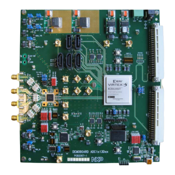
- Page 3 1. Quick start 1.1 Setup overview Fig 1 presents the connections to measure the ADC1x13Dxxx DC Power supply for complete board (5V/2A) Output connector for parallel data INPUT-A CLK-P Clock and signal CLK-N Optional : Generator FPGA Clock inputs INPUT-B USB port for connection to PC (USB and SPI...
- Page 5 1.2 Essential Features of the Demonstration Board Fig 2.ADC1413D125 with 2 lanes in pairs of CML compliant differential Fig. 2 shows the ADC1413D125 in its environment. The output is a series CML connection capable of delivering a throughput rate of 3.125Gsps as specified by the JESD204A standard. The input is connected through an SMA connector and 2 transformers to adapt the impedance and create a differential input to the ADC The logic device Field Programmable Gate Array (FPGA) is connected to the ADC1413D125D via...
-
Page 6: Flash Memory
D11 lights up: FPGA has up-loaded its bit-stream Flash Memory D12 lights up: USB Host detected Mini USB connector Fig 4. On board memory with LED D11 indicating FPGA up-loaded and running and D12 indicating USB host detected Furthermore, after connecting the USB port and installing the driver, the LED D12 indicates that the USB host has been detected and is up and running. - Page 7 Fig 6. shows the LEDs D9-D16 which are used to indicate the status of the FPGA. FPGA clk heart beat Sync signal is active K28.5 received 14 bits Data are reverted 8bits by 8 bits Fig 6. D13 – D16 indicates the status of the FPGA PUSH-A Perform a Manual Synchronization between FPGA and ADC...
- Page 8 Clock signal Clock Generator coming from one generator CML/LVDS and fed to J19 Direct input and CLKP available Fig 7. Clock Inputs Remark: as the clock can come either internally or externally, multiplexers are available so as to route the right clock signal to the devices, the ADC1413D125 and the FPGA. When using an external clock the double switch SW5 should be set to the “ON”...
- Page 9 2. Example 2.1 Setup example DC adaptor connected to mains SMA 100 A Rohde & Schwarz Signal Generator USB SPI SMA 100 A ADC1413D125. Rohde & Schwarz Register Clock Generator programming Data Acquisition and processing Fig 9. ADC1413D125D Demonstrator Hardware set...
- Page 10 3. SPI quick start 3.1 Install The demonstration board is delivered with the following software: Labview Runtime: LabVIEW85RuntimeEngineFull.exe Labview executable: Andromeda.exe Appropriate drivers • Step 1 Connect the device to a USB port on your PC. Windows ‘Found New Hardware Wizard’ will be launched. Select ‘No, not this time’...
- Page 11 • Step 2 Select ‘Install from a list or specific location (Advanced)’ as shown below and then click ‘Next’. • Step 3 Select ‘Search for the best driver in these locations’ and enter the file path of the folder CD-ROM CONTENT\CD-ROM2_ADC1213d_ADC1413d_DAC1408d\Version_1.0\Driver USB \driver_d2xx’ in the combo-box (‘C:\driver_2xx’...
- Page 12 • Step 4 Windows should then display a message indicating that the installation was successful. Click ‘Finish’ to complete the installation for the first port of the device.
-
Page 13: Spi Interface
3.2 SPI interface • Step 1 LabVIEW85RuntimeEngineFull.exe Install the LabVIEW Run-time Engine (if not already installed). • Step 2 Start the LabVIEW application “ADC1x13.exe”. a graphical window will pop-up Under the “ Write register from command file” field, choose the write configuration file from “ADC Command” directory depending on the used operating points. - Page 14 Click on ADC button to choose between internal ADC capture or FPGA capture Click on Load DATA to get the FFT and the ADC performances...
- Page 15 Load Data to start Select FFT without window capturing (Clock coherency OK) Select the wanted ADC input channel. « latest MRA » button must be green Check input level here Select Input Frequency = 150M ADC clock = 76.8M Select « use coherence » when clock input coherence is OK in order to get SFDR value calculation...
Need help?
Do you have a question about the ADC1 13D Series and is the answer not in the manual?
Questions and answers