Table of Contents
Advertisement
Quick Links
VICTOR COMPANY OF JAPAN, LIMITED
VIDEO DIVISION
SERVICE MANUAL
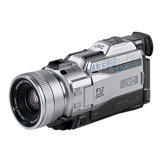
GR-DV3000A/EA/ED/EG/EK/SH
SPECIFICATIONS
Power supply
: DC 6.3 V
Power consumption
LCD monitor off, viewfinder on : Approx. 4.3 W
LCD monitor on, viewfinder off : Approx. 5.4 W
Dimensions (W x H x D)
: 76 mm x 90 mm x 194 mm
Weight
: Approx. 660 g (without cassette, memory card and battery)
Operating temperature
: 0°C to 40°C
Operating humidity
: 35% to 80%
Storage temperature
: –20°C to 50°C
Pickup
: 1/3.6" CCD
Lens
: F 1.2, f = 4.5 mm to 45 mm, 10:1 power zoom lens
Filter diameter
: ø52 mm
LCD monitor
: 3.5" diagonally measured, LCD panel/TFT active matrix system
Viewfinder
: Electronic viewfinder with 0.44" colour LCD
Speaker
: Monaural
Format
: DV format (SD mode)
Signal format
: PAL standard
Recording/Playback format
: Video: Digital component recording
: Audio: PCM digital recording, 32 kHz 4-channel (12-bit),
Cassette
: Mini DV cassette
Tape speed
: SP: 18.8 mm/s
Maximum recording time
: SP: 80 min.
(using 80 min. cassette)
Digital Still Camera Function
Storage media
: SD Memory Card/MultiMediaCard
Compression system
: Still image
File size
: Still image
Picture quality
: 2 modes (FINE/STANDARD)
Approximate number of storable images
(with the provided memory card [8 MB])
FINE
: 32 (640 x 480 pixels), 14 (1024 x 768 pixels),
S40894
STANDARD
: 110 (640 x 480 pixels), 46 (1024 x 768 pixels),
For other memory cards,
pg. 17.
Printed in Japan
DIGITAL VIDEO CAMERA
(The specifications shown pertain specifically to the model GR-DV3000EG/EK)
Camcorder
AV
General
Video output
Video input
Audio output
(Using AC Power Adapter/Charger)
Audio input
DC 7.2 V
(Using battery pack)
DV
Input/output
PHONE
Headphone output
PRINTER
(with the LCD monitor closed and the viewfinder pushed back in,
without the lens hood)
Approx. 740 g (incl. cassette, memory card and battery)
AC Power Adapter/Charger AA-V40EG or AA-V40EK
Power requirement
Power consumption
Output
Charge
VTR
Dimensions (W x H x D)
Weight
AA-V40EG
Digital Video Camera
AA-V40EK
48 kHz 2-channel (16-bit)
Dimensions (W x H x D)
LP: 12.5 mm/s
Weight
LP: 120 min.
USB
S-VIDEO
: JPEG (compatible)
Output
Moving image : MPEG4 (compatible)
: 4 modes (1600 x 1200 pixels, 1280 x 960 pixels,
Input
1024 x 768 pixels, 640 x 480 pixels)
Moving image : 2 modes (240 x 176 pixels, 160 x 120 pixels)
EDIT
Specifications shown are for SP mode unless otherwise indicated. E & O.E. Design and
9 (1280 x 960 pixels), 6 (1600 x 1200 pixels)
specifications subject to change without notice.
30 (1280 x 960 pixels), 20 (1600 x 1200 pixels)
This service manual is printed on 100% recycled paper.
COPYRIGHT © 2002 VICTOR COMPANY OF JAPAN, LTD.
Connectors
: 1 V (p-p), 75 Ω, analogue
: 0.5 V (p-p) – 2.0 V (p-p), 75 Ω, analogue
: 300 mV (rms), 1 kΩ, analogue, stereo
: 300 mV (rms), 50 kΩ, analogue, stereo
: 4-pin, IEEE 1394 compliant
: ø3.5 mm, stereo
: For an optional video printer equipped with a PRINT DATA
connector
: AC 110 V to 240 V`, 50 Hz/60 Hz
: 23 W
: DC 7.2 V
, 1.2 A
: DC 6.3 V
, 1.8 A
: 68 mm x 38 mm x 110 mm
: Approx. 260 g
: Approx. 340 g
Jack Box CU-V504U
General
: 37.5 mm x 18.5 mm x 55 mm
: Approx. 30 g
Connectors
: TYPE B
: Y: 1 V (p-p), 75 Ω, analogue
C: 0.29 V (p-p), 75 Ω, analogue
: Y: 0.8 V (p-p) – 1.2 V (p-p), 75 Ω, analogue
C: 0.2 V (p-p) – 0.4 V (p-p), 75 Ω, analogue
: ø3.5 mm, 2-pole
No. 86666
January 2002
Advertisement
Table of Contents

Related Manuals for JVC GR-DV3000A


Summary of Contents for JVC GR-DV3000A
- Page 1 SERVICE MANUAL DIGITAL VIDEO CAMERA GR-DV3000A/EA/ED/EG/EK/SH SPECIFICATIONS (The specifications shown pertain specifically to the model GR-DV3000EG/EK) Camcorder Connectors General : 1 V (p-p), 75 Ω, analogue Video output : 0.5 V (p-p) – 2.0 V (p-p), 75 Ω, analogue Video input Audio output : 300 mV (rms), 1 kΩ, analogue, stereo...
-
Page 2: Table Of Contents
FE SW BOARD ASSEMBLY <11> .......... 5-23 FRONT BOARD ASSEMBLY <12> ......... 5-23 VF BL BOARD ASSEMBLY <13> ..........5-23 The following table lists the differing points between Models GR-DV3000EG, GR-DV3000EK, GR-DV3000EA, GR-DV3000A, GR-DV3000SH and GR-DV3000ED in this serise. GR-DV3000EG... - Page 3 Important Safety Precautions Prior to shipment from the factory, JVC products are strictly inspected to conform with the recognized product safety and electrical codes of the countries in which they are to be sold. However, in order to maintain such compliance, it is equally important to implement the following precautions when a set is being serviced.
- Page 4 • Safety Check after Servicing Examine the area surrounding the repaired location for damage or deterioration. Observe that screws, parts and wires have been returned to original positions, Afterwards, perform the following tests and confirm the specified values in order to verify compliance with safety standards.
-
Page 5: Disassembly
SECTION 1 DISASSEMBLY 1.1 BEFORE ASSEMBLY AND DISASSEMBLY 1.1.4 Disconnection of Connectors (Wires) 1.1.1 Precautions Connector Pull both ends of the connector in the arrow direction, re- 1. Be sure to remove the power supply unit prior to mount- move the lock and disconnect the flat wire. ing and soldering of parts. -
Page 6: Jigs And Tools Required For Disassembly, Assembly And Adjustment
1.2 JIGS AND TOOLS REQUIRED FOR DISASSEMBLY, 1.3 DISASSEMBLY/ASSEMBLY OF CABINET PARTS ASSEMBLY AND ADJUSTMENT AND BOARD ASSEMBLY 1.2.1 Tools required for adjustments 1.3.1 Disassembly flow chart This flowchart indicates the disassembly step for the cabi- Torque driver YTU94088 YTU94088-003 net parts and board assembly in order to gain access to item(s) to be serviced. -
Page 7: Disassembly Method
1.3.2 Disassembly method NOTE a: Open the cassette cover after removing the STEP Fig.No. PART POINT NOTE screws. ZOOM OPE UNIT Fig.1-3-1 3(S1),(L1a),5(L1b),CN1a NOTE b: Be sure to confirm the position of the screws. FRONT COVER Fig.1-3-2a CN2a,CN2b,2(S2a),(S2b), NOTE2a NOTE c: Be careful not to damage the FPC when unplug- ASSY (S2c),(S2d),2(S2e),CN2c... - Page 8 JUNCTION BOARD ASSY NOTE FE SW BOARD ASSY NOTE FRONT BOARD ASSY WIRERING WIRE Fig. 1-3-1 Fig. 1-3-2b NOTE NOTE NOTE NOTE NOTE (BOTTOM) NOTE NOTE Fig. 1-3-2a...
- Page 9 SHOE ASSY FOCUS UNIT SW FPC UNIT COVER (MENU) MICROPHONE Fig. 1-3-2c NOTE 3 b NOTE 3 b NOTE 3 b NOTE 3 c NOTE 3 a NOTE 3 a (BOTTOM) NOTE 3 c Fig. 1-3-3...
- Page 10 NOTE 4 Fig. 1-3-4 Fig. 1-3-6 NOTE 7 NOTE 5 Fig. 1-3-5 Fig. 1-3-7...
- Page 11 Fig. 1-3-8 Fig. 1-3-9 NOTE NOTE CN407 NOTE CN403 SHIELD COVER (PRE/REC) ∗ ∗ ∗ ∗ ∗ NOTE BKT (MECHA) ASSY ∗ : 0.069 N • m (0.7 kgf • Fig. 1-3-10...
-
Page 12: Precautions
1.4 DISASSEMBLY OF THE OP BLOCK AND CCD 1.4.3 How to install BOARD ASSEMBLIES 1. With the spacer rubbers attached to the CCD base, 1.4.1 Precautions mount the CCD base in the OP Block Assembly and tighten them together using the two screws (1, 2). 1. -
Page 13: Vf(Color)
E.VF(COLOR) 1.5.1. Disassembly/Assembly of the E.VF(COLOR) 1. Remove the two screws (1 and 2) and then remove the EYE CUP. 2. Remove the two screws (3 and 4). 3. Pull out the VF assembly and then remove the three screws (5 to 7) to release the FPC ASSY. 4. -
Page 14: Disassembly/Assembly Of The 7 E.vf(Color)
1.6 DISASSEMBLY/ASSEMBLY OF THE MONITOR a: Be careful not to damage the FPC or the connec- Note ASSEMBLY tor when removing the Monitor Cover Assembly. Note b: Be careful not to damage the parts when remov- 1.6.1 Monitor Assembly and Hinge Assembly ing or mounting the Hinge Assembly. -
Page 15: Manual Ejection Of The Cassette Tape
1.7 MANUAL EJECTION OF THE CASSETTE TAPE 4. In order to change the mechanism mode at the unload- Note: The following procedure describes a simplified method ing end apply 3 V, DC to the electrode on the top sur- of ejecting the cassette tape in case it is not possible face of the Loading Motor Assembly and then set it to to eject it, due to an electrical failure. -
Page 16: Emergency Display
1.8 EMERGENCY DISPLAY Whenever some abnormal signal is input to the syscon Example (in case of the error number E01): CPU, an error number (E01, as an example) is displayed on the LCD monitor or (in the electronic view finder). In every error status, such the message as shown below alternately appear over and over. -
Page 17: Service Note
1.9 SERVICE NOTE 1-13... -
Page 18: Mechanism Adjustment
SECTION 2 MECHANISM ADJUSTMENT 2.1 PRELIMINARY REMARKS ON ADJUSTMENT AND (3) The symbol (T or B)appearing in this column shows the REPAIR side which the objective part is mounted on. T =the upper side, B =the lower side 2.1.1 Precautions (4) Symbols appearing in this column indicate drawing 1. -
Page 19: Jigs And Tools Required For Disassembly, Assembly And Adjustment
2.2 JIGS AND TOOLS REQUIRED FOR DISASSEMBLY, ASSEMBLY AND ADJUSTMENT 2.2.1 Tools required for adjustments 1. Torque driver Torque driver YTU94088 YTU94088-003 Be sure to use to fastening the mechanism and exterior parts because those parts must strictly be controlled for tightening torque. -
Page 20: Disassembly/Assembly Of Mechanism Assembly
2.3 DISASSEMBLY/ASSEMBLY OF MECHANISM AS- 2.3.2 Explanation of mechanism mode SEMBLY The mechanism mode of this model is classified into five 2.3.1 General statement modes as shown in Table 2-3-1. Each mechanism mode can be distinguished from others by the relative position The mechanism should generally be disassembled/assem- of “... -
Page 21: Mechanism Timing Chart
2.3.3 Mechanism timing chart MODE SHORT TU. P. B SLIDE TU. P. B SLIDE RELEASE EJECT CAS. IN START START STOP PLAY PARTS MAIN CAM -12.40° 0° (22.44°) 58.71° (69.53°) (80.5°) (150.58°) (153.5°) 177.79° 212.77° 243.94° SUB CAM -16.97° 0° (30.71°) 80.34°... -
Page 22: Disassembling Procedure Table
2.4 DISASSEMBLING PROCEDURE TABLE MARK: After assembly, perform adjustments. PART NAME FIG. POINT NOTE REMARKS CASSETTE HOUSING ASSY Fig.2-4-3 ),(L a)-(L NOTE a,b,c,d ADJUSTMENT UPPER BASE ASSY Fig.2-4-4 ),(L a),(L NOTE DRUM ASSY a),2(S NOTE REEL DISK ASSY(SUP) Fig.2-4-5 NOTE REEL DISK ASSY(TU) NOTE REEL COVER ASSY... - Page 23 < TOP VIEW > 24 27 36 35 Fig. 2-4-1 < BOTTOM VIEW > 31 16 Fig. 2-4-2...
-
Page 24: Disassembly/Assembly
2.4.1 Disassembly/assembly CASSETTE HOUSING ASSY NOTE NOTE Be careful not to damage any of the parts during work. NOTE NOTE NOTE Special care is required in mounting. NOTE NOTE LOCK When mounting, the CASSETTE NOTE LEVER HOUSING ASSY should be at- NOTE tached in the Eject status. - Page 25 REEL DISK ASSY(SUP) REEL DISK ASSY(TU) REEL COVER ASSY NOTE NOTE Be careful not to attach the REEL DISK wrongly. The Sup- NOTE ply side can be identified by the white color at the center. NOTE NOTE REEL DISK ASSY Be careful not to attach the REEL DISK wrongly.
- Page 26 SLIDE DECK ASSY NOTE Each of the parts on the SLIDE DECK ASSY can be re- placed separately. When detaching the assembly, if there is no need to replace any of its parts, remove the SLIDE DECK ASSY as it is. NOTE When mounting, pay attention to the positions of the ¤...
- Page 27 TENSION CTL LEVER ASSY CENTER GEAR & PINCH ROLLER ARM F. ASSY TENSION CTL PLATE ASSY BRAKE CTL LEVER ASSY NOTE NOTES When mounting, pay attention to the correct positioning. NOTE NOTE NOTE (TOP) NOTE (BOTTOM) NOTE NOTES When mounting, pay atten- &...
- Page 28 fl BASE R ASSY ‡ ROTARY ENCODER ° GEAR COVER ASSY · MAIN CAM ASSY NOTE fl NOTE NOTE When mounting, fold the sliding part to the inner side. ‡ NOTE NOTE When mounting, pay attention to the correct positioning and the FPC layout.
- Page 29 ∞ DRUM BASE ASSY § CAPSTAN MOTOR ¶ MAIN DECK ASSY ∞ § NOTES When detaching, remove them together and then separate § from ∞ a. ∞ NOTE When mounting, attach the DRUM BASE ASSY so that the screw hole is located at the center of the ellipse. NOTE NOTE NOTE...
-
Page 30: List Of Procedures For Disassembly
2.4.2 List of procedures for disassembly Fig. 2-4-13 2-13... -
Page 31: Checkup And Adjustment Of Mechanism Phase
2.5 CHECKUP AND ADJUSTMENT OF MECHANISM PHASE MODE GEAR ROTARY ENCODER Align the MODE GEAR with the Main Deck Mount the ROTARY ENCODER by aligning its mark ( Assembly hole. and the mark ( ) of the Main Deck Assembly. Note: Note: Be careful when handling the FPC during mounting. -
Page 32: Mechanism Adjustments
2.6 MECHANISM ADJUSTMENTS 2.6.1 Adjustment of the slide guide plate Use Fig. 2-6-1 as the reference unless otherwise specified. 1. Set the PLAY mode. See Fig. 2-3-8. 2. Loosen the screws ( A , B ). 3. With the Main Deck and Slide Deck Assemblies pushed into the unit, tighten the screws ( A , B ) while applying pressure to the stud (shaft) on the Slide Guide plate. -
Page 33: Adjustment Of The Tension Arm And Pad Arm Assemblies
2.6.2 Adjustment of the Tension Arm and Pad Arm As- 2.6.3 Adjustment of the Slide Lever 2 semblies Use Fig. 2-6-3 as the reference unless otherwise specified. Use Fig. 2-6-2 as the reference unless otherwise specified. 1. Set the C IN mode. 1. -
Page 34: Service Note
2.7 SERVICE NOTE Use the following chart to manage mechanism parts that are removed for disassembling the mechanism. Fig. Fig. CASSETTE HOUSING ASSY UPPER BASE ASSY Fig. Fig. REEL DISK ASSY(SUP) REEL COVER ASSY DRUM ASSY REEL DISK ASSY(TU) Fig. TENSION ARM ASSY SLANT POLE ARM ASSY TU ARM ASSY... - Page 35 Fig. PINCH ROLLER TENSION BRAKE CTL TENSION CTL CENTER GEAR ARM F. ASSY CTL PLATE LEVER LEVER ASSY ASSY ASSY Fig. MOTOR GUIDE SLIDE LEVER 2 LOADING BRACKET RAIL ASSY ASSY PLATE ASSY ASSY MODE GEAR EJECT LEVER Fig. BASE R ASSY ROTARY GEAR COVER MAIN CAM ASSY...
-
Page 36: Jig Connector Cable Connection
2.8 JIG CONNECTOR CABLE CONNECTION Remove one screw (1) first and the cover (JIG) next. COMMUNICATION CABLE JIG CONNECTOR to 8 pin ( JLIP_RX ) to 9 pin JACK BOX WHITE ( JLIP_TX ) to 5 or 23 pin BLACK ( GND ) COVER CN107... -
Page 37: Tape Pattern Check
2.8.1 Tape pattern check (1) Play back the compatibility adjustment tape. (2) While triggering the MAIN CN107-10PIN (HID1), ob- CN107 serve the waveform of CN107-26PIN (ENV_OUT). (ENV_OUT) (3) Confirm that the waveform is free from remarkable level-down, and entirely parallel and straight. Moreover, perform the following adjustment as re- CN107 quired. -
Page 38: Electrical Adjustment
SECTION 3 ELECTRICAL ADJUSTMENT 3.1 PRECAUTION 3. Tools required for adjustments 1. Precaution Torque driver YTU94088 YTU94088-003 Both the camera and deck sections of this model needs a personal computer for adjustment except simple adjustment with potentiometers. If some of the following parts is replaced for repair or other reason, the repaired set must be adjusted with a personal computer. -
Page 39: Setup
Torque driver PC cable Be sure to use to fastening the mechanism and exte- To be used to connect the VideoMovie and a personal rior parts because those parts must strictly be control- computer with each other when a personal computer led for tightening torque. -
Page 40: Monitor Adjustment
3.3 MONITOR ADJUSTMENT 3.4 ELECTRONIC VIEWFINDER (E.VF) ADJUSTMENT Notes : Unless otherwise specified, all measurement points Notes : Unless otherwise specified, all measurement points and adjustment parts are located on MONITOR and adjustment parts are located on MONITOR board. board. 3.3.1 PLL (MONI) 3.4.1 PLL (VF) •... -
Page 41: Packing And Accessory Assembly
LYT0884-006A INST.BOOK(PRINTER.SP),A LYT0939-015A INST.BOOK(PRINTER.GE),A,C,G LYT0939-016A INST.BOOK(PRINTER.DU),A MODEL MARK LYT0939-017A INST.BOOK(PRINTER.IT),A GR-DV3000EG-X LYT0939-018A INST.BOOK(PRINTER.DA),G LYT0939-019A INST.BOOK(PRINTER.FI),G GR-DV3000EK FINAL ASSY LYT0939-020A INST.BOOK(PRINTER.SW),G GR-DV3000A <M2> LYT0939-021A INST.BOOK(PRINTER.NO),G LYT0972-005A INST.BOOK(PRINTER.CH),C,E,F GR-DV3000EA LYT0972-006A INST.BOOK(PRINTER.RU),C,E,F GR-DV3000ED LYT0972-007A INST.BOOK(PRINTER.AR),C LYT0883-002A INST.BOOK(SOFT.GE),A,C,G GR-DV3000SH LYT0883-004A INST.BOOK(SOFT.DU),A GR-DV3000EG-Y LYT0883-006A INST.BOOK(SOFT.IT),A LYT0883-007A INST.BOOK(SOFT.DA),G... - Page 42 FINAL ASSEMBLY <M2> ELECTRONIC VIEWFINDER 101A <M4> 101E 216E 216C 101F JACK 101G 101C 216E <07> 101D 101G 101B 101B 121A 216D RATING LABEL <05> 216A 216B 121A 251G 231A 251G <10> 231A 121B EJECT <08> 251F MECHANISM 251E <M3> 251D 143A PRE/MDA...
- Page 43 REF No. PART No. PART NAME, DESCRIPTION REF No. PART No. PART NAME, DESCRIPTION - - - - - - - - - - - - - - - - - - - - - - - - - - - - - - - - - - - - - - - - - - - - - - - - - - - - - - - - - - - - - - - - - - - - - - - - - - - - - - - - - - - - - - - - - - - - - - - - - - - - - - - - - - - - - - - - - - - - - - - - - - - - - - - - - - - -...
- Page 44 MECHANISM ASSEMBLY <M3> 436B 436B 436A Classification Part No. Symbol in drawing Grease KYODO-SH-JB NOTE:The section marked in AA and BB, CC indicate YTU94027 lubrication and greasing areas. Grease RX-410R (HANARL)
-
Page 45: Mechanism Assembly
REF No. PART No. PART NAME, DESCRIPTION REF No. PART No. PART NAME, DESCRIPTION - - - - - - - - - - - - - - - - - - - - - - - - - - - - - - - - - - - - - - - - - - - - - - - - - - - - - - - - - - - - - - - - - - - - - - - - - - - - - - - - - - - - - - - - - - - - - - - - - - - - - - - - - - - - - - - - - - - - - - - - - - - - - - - - - - - -... -
Page 46: Electronic Viewfinder Assembly
ELECTRONIC VIEWFINDER ASSEMBLY <M4> VF BL <13> REF No. PART No. PART NAME, DESCRIPTION REF No. PART No. PART NAME, DESCRIPTION - - - - - - - - - - - - - - - - - - - - - - - - - - - - - - - - - - - - - - - - - - - - - - - - - - - - - - - - - - - - - - - - - - - - - - - - - - - - - - - - - - - - - - - - - - - - - - - - - - - - - - - - - - - - - - - - - - - - - - - - - - - - - - - - - -... -
Page 47: Monitor Assembly
MONITOR ASSEMBLY <M5> 501A 501B 501G 501C 501F 501D 501E 501E MONITOR <06> 502B 502A REF No. PART No. PART NAME, DESCRIPTION REF No. PART No. PART NAME, DESCRIPTION - - - - - - - - - - - - - - - - - - - - - - - - - - - - - - - - - - - - - - - - - - - - - - - - - - - - - - - - - - - - - - - - - - - - - - - - - - - - - - - - - - - - - - - - - - - - - - - - - - - - - - - - - - -... -
Page 48: Electrical Parts List
ELECTRICAL PARTS LIST REF No. PART No. PART NAME, DESCRIPTION REF No. PART No. PART NAME, DESCRIPTION - - - - - - - - - - - - - - - - - - - - - - - - - - - - - - - - - - - - - - - - - - - - - - - - - - - - - - - - - - - - - - - - - - - - - - - - - - - - - - - - - - - - - - - - - - - - - - - - - - - - - - - - - - - - - - - - - - - - - - - - - - - - - - - - - - - -... - Page 49 REF No. PART No. PART NAME, DESCRIPTION REF No. PART No. PART NAME, DESCRIPTION - - - - - - - - - - - - - - - - - - - - - - - - - - - - - - - - - - - - - - - - - - - - - - - - - - - - - - - - - - - - - - - - - - - - - - - - - - - - - - - - - - - - - - - - - - - - - - - - - - - - - - - - - - - - - - - - - - - - - - - - - - - - - - - - - - - -...
- Page 50 REF No. PART No. PART NAME, DESCRIPTION REF No. PART No. PART NAME, DESCRIPTION - - - - - - - - - - - - - - - - - - - - - - - - - - - - - - - - - - - - - - - - - - - - - - - - - - - - - - - - - - - - - - - - - - - - - - - - - - - - - - - - - - - - - - - - - - - - - - - - - - - - - - - - - - - - - - - - - - - - - - - - - - - - - - - - - - - -...
- Page 51 REF No. PART No. PART NAME, DESCRIPTION REF No. PART No. PART NAME, DESCRIPTION - - - - - - - - - - - - - - - - - - - - - - - - - - - - - - - - - - - - - - - - - - - - - - - - - - - - - - - - - - - - - - - - - - - - - - - - - - - - - - - - - - - - - - - - - - - - - - - - - - - - - - - - - - - - - - - - - - - - - - - - - - - - - - - - - - - -...
- Page 52 REF No. PART No. PART NAME, DESCRIPTION REF No. PART No. PART NAME, DESCRIPTION - - - - - - - - - - - - - - - - - - - - - - - - - - - - - - - - - - - - - - - - - - - - - - - - - - - - - - - - - - - - - - - - - - - - - - - - - - - - - - - - - - - - - - - - - - - - - - - - - - - - - - - - - - - - - - - - - - - - - - - - - - - - - - - - - - - -...
- Page 53 REF No. PART No. PART NAME, DESCRIPTION REF No. PART No. PART NAME, DESCRIPTION - - - - - - - - - - - - - - - - - - - - - - - - - - - - - - - - - - - - - - - - - - - - - - - - - - - - - - - - - - - - - - - - - - - - - - - - - - - - - - - - - - - - - - - - - - - - - - - - - - - - - - - - - - - - - - - - - - - - - - - - - - - - - - - - - - - -...
- Page 54 REF No. PART No. PART NAME, DESCRIPTION REF No. PART No. PART NAME, DESCRIPTION - - - - - - - - - - - - - - - - - - - - - - - - - - - - - - - - - - - - - - - - - - - - - - - - - - - - - - - - - - - - - - - - - - - - - - - - - - - - - - - - - - - - - - - - - - - - - - - - - - - - - - - - - - - - - - - - - - - - - - - - - - - - - - - - - - - -...
-
Page 55: Dsc Board Assembly <02
REF No. PART No. PART NAME, DESCRIPTION REF No. PART No. PART NAME, DESCRIPTION - - - - - - - - - - - - - - - - - - - - - - - - - - - - - - - - - - - - - - - - - - - - - - - - - - - - - - - - - - - - - - - - - - - - - - - - - - - - - - - - - - - - - - - - - - - - - - - - - - - - - - - - - - - - - - - - - - - - - - - - - - - - - - - - - - - -... -
Page 56: Pre/Mda Board Assembly <03
REF No. PART No. PART NAME, DESCRIPTION REF No. PART No. PART NAME, DESCRIPTION - - - - - - - - - - - - - - - - - - - - - - - - - - - - - - - - - - - - - - - - - - - - - - - - - - - - - - - - - - - - - - - - - - - - - - - - - - - - - - - - - - - - - - - - - - - - - - - - - - - - - - - - - - - - - - - - - - - - - - - - - - - - - - - - - - - -... -
Page 57: Junction Board Assembly <04
REF No. PART No. PART NAME, DESCRIPTION REF No. PART No. PART NAME, DESCRIPTION - - - - - - - - - - - - - - - - - - - - - - - - - - - - - - - - - - - - - - - - - - - - - - - - - - - - - - - - - - - - - - - - - - - - - - - - - - - - - - - - - - - - - - - - - - - - - - - - - - - - - - - - - - - - - - - - - - - - - - - - - - - - - - - - - - - -... -
Page 58: Monitor Board Assembly <06
REF No. PART No. PART NAME, DESCRIPTION REF No. PART No. PART NAME, DESCRIPTION - - - - - - - - - - - - - - - - - - - - - - - - - - - - - - - - - - - - - - - - - - - - - - - - - - - - - - - - - - - - - - - - - - - - - - - - - - - - - - - - - - - - - - - - - - - - - - - - - - - - - - - - - - - - - - - - - - - - - - - - - - - - - - - - - - - -... - Page 59 REF No. PART No. PART NAME, DESCRIPTION REF No. PART No. PART NAME, DESCRIPTION - - - - - - - - - - - - - - - - - - - - - - - - - - - - - - - - - - - - - - - - - - - - - - - - - - - - - - - - - - - - - - - - - - - - - - - - - - - - - - - - - - - - - - - - - - - - - - - - - - - - - - - - - - - - - - - - - - - - - - - - - - - - - - - - - - - -...
-
Page 60: Jack Board Assembly <07
REF No. PART No. PART NAME, DESCRIPTION REF No. PART No. PART NAME, DESCRIPTION - - - - - - - - - - - - - - - - - - - - - - - - - - - - - - - - - - - - - - - - - - - - - - - - - - - - - - - - - - - - - - - - - - - - - - - - - - - - - - - - - - - - - - - - - - - - - - - - - - - - - - - - - - - - - - - - - - - - - - - - - - - - - - - - - - - -... -
Page 61: Ccd Board Assembly <10
REF No. PART No. PART NAME, DESCRIPTION REF No. PART No. PART NAME, DESCRIPTION - - - - - - - - - - - - - - - - - - - - - - - - - - - - - - - - - - - - - - - - - - - - - - - - - - - - - - - - - - - - - - - - - - - - - - - - - - - - - - - - - - - - - - - - - - - - - - - - - - - - - - - - - - - - - - - - - - - - - - - - - - - - - - - - - - - -... - Page 62 SECTION 4 CIRCUIT BOARD NOTES CHARTS AND DIAGRAMS 1. Foil and Component sides 1) Foil side (B side) : NOTES OF SCHEMATIC DIAGRAM 4. Voltage measurement Parts on the foil side seen from foil face (pattern face) 1) Regulator (DC/DC CONV) circuits are indicated.
- Page 63 ∗ NOTE ) : The number of patch cords BOARD INTERCONNECTIONS are indicated by interconnected. ∗ YTU94074-8 ∗ YTU94074-24 YTU94077-8 FOCUS UNIT YTU94077-24 (Page 4-48) VF_UNIT ∗ DECK OPE. YTU94074-6 YTU94077-6 ∗ S2401 (Page 4-45) YTU94074-22 1 0 CCD MAIN LCD MODULE IR_UNIT YTU94077-22...
- Page 64 MAIN IF SCHEMATIC DIAGRAM NOTES : For the destination of each signal and further line connections that are cut off from TO JUNCTION CN1101 MAIN TO SHOE FPC this diagram , refer to "4.1 BOARD INTERCONNECTIONS". CN103 CN114 CN112 When ordering parts , be sure to order according to the Part Number indicated in the Parts List. QGF0517F2-16X QGF0505F1-16X ∗...
- Page 65 NOTES : For the destination of each signal and further line connections that are cut off from SYSCON-CPU SCHEMATIC DIAGRAM this diagram , refer to "4.1 BOARD INTERCONNECTIONS". When ordering parts , be sure to order according to the Part Number indicated in the Parts List. 0 1 MAIN (SYSCON-CPU) MSD-CPU SRV_RST...
- Page 66 NOTES : For the destination of each signal and further line connections that are cut off from MSD-CPU SCHEMATIC DIAGRAM this diagram , refer to "4.1 BOARD INTERCONNECTIONS". When ordering parts , be sure to order according to the Part Number indicated in the Parts List. 0 1 MAIN (MSD-CPU) MAIN IF CN109...
- Page 67 NOTES : For the destination of each signal and further line connections that are cut off from AUDIO AD/DA SCHEMATIC DIAGRAM this diagram , refer to "4.1 BOARD INTERCONNECTIONS". When ordering parts , be sure to order according to the Part Number indicated in the Parts List. MAIN (AUDIO AD/DA) DVMAIN AIBCK...
- Page 68 NOTES : For the destination of each signal and further line connections that are cut off from MAIN AUDIO SCHEMATIC DIAGRAM this diagram , refer to "4.1 BOARD INTERCONNECTIONS". When ordering parts , be sure to order according to the Part Number indicated in the Parts List. 0 1 MAIN (MAIN AUDIO) AUDIO AD/DA...
- Page 69 DVMAIN SCHEMATIC DIAGRAM NOTES : For the destination of each signal and further line connections that are cut off from this diagram , refer to "4.1 BOARD INTERCONNECTIONS". When ordering parts , be sure to order according to the Part Number indicated in the Parts List. MAIN (DVMAIN) C3041 C3040...
- Page 70 NOTES : For the destination of each signal and further line connections that are cut off from this diagram , refer to "4.1 BOARD INTERCONNECTIONS". VIDEO I/O SCHEMATIC DIAGRAM When ordering parts , be sure to order according to the Part Number indicated in the Parts List. MAIN(VIDEO I/O) L3701 10µ...
- Page 71 CDS/AD SCHEMATIC DIAGRAM NOTES : For the destination of each signal and further line connections that are cut off from this diagram , refer to "4.1 BOARD INTERCONNECTIONS". When ordering parts , be sure to order according to the Part Number indicated in the Parts List. 0 1 MAIN(CDS/AD) IC4202 RH5RZ31CA-X...
- Page 72 NOTES : For the destination of each signal and further line connections that are cut off from 4.10 DSP SCHEMATIC DIAGRAM this diagram , refer to "4.1 BOARD INTERCONNECTIONS". When ordering parts , be sure to order according to the Part Number indicated in the Parts List. X4301 0 1 MAIN(DSP) NAX0319-001X...
- Page 73 4.11 OP DRIVE SCHEMATIC DIAGRAM NOTES : For the destination of each signal and further line connections that are cut off from this diagram , refer to "4.1 BOARD INTERCONNECTIONS". When ordering parts , be sure to order according to the Part Number indicated in the Parts List. 0 1 MAIN(OP DRIVE) IC4807 R4839...
- Page 74 4.12 TG/VDR SCHEMATIC DIAGRAM NOTES : For the destination of each signal and further line connections that are cut off from this diagram , refer to "4.1 BOARD INTERCONNECTIONS". When ordering parts , be sure to order according to the Part Number indicated in the Parts List. 0 1 MAIN(TG/VDR) TG_RST CLK_OUT...
- Page 75 NOTES : For the destination of each signal and further line connections that are cut off from 4.13 DSC SCHEMATIC DIAGRAM this diagram , refer to "4.1 BOARD INTERCONNECTIONS". When ordering parts , be sure to order according to the Part Number indicated in the Parts List. 0 2 DSC(DSC) DSC IF CN8401...
- Page 76 4.14 DSC IF AND SD SCHEMATIC DIAGRAMS - DSC IF - NOTES : For the destination of each signal and further line connections that are cut off from this diagram , refer to "4.1 BOARD INTERCONNECTIONS". TO MAIN IF CN105 CN8401 QGB0516M1-80X When ordering parts , be sure to order according to the Part Number indicated in the Parts List.
- Page 77 4.15 USB SCHEMATIC DIAGRAM NOTES : For the destination of each signal and further line connections that are cut off from this diagram , refer to "4.1 BOARD INTERCONNECTIONS". When ordering parts , be sure to order according to the Part Number indicated in the Parts List. 0 2 DSC(USB) TO DSC GIO3...
- Page 78 4.16 MDA SCHEMATIC DIAGRAM NOTES : For the destination of each signal and further line connections that are cut off from this diagram , refer to "4.1 BOARD INTERCONNECTIONS". When ordering parts , be sure to order according to the Part Number indicated in the Parts List. TO MAIN IF CN106 CN401...
- Page 79 4.17 PRE/REC SCHEMATIC DIAGRAM NOTES : For the destination of each signal and further line connections that are cut off from this diagram , refer to "4.1 BOARD INTERCONNECTIONS". When ordering parts , be sure to order according to the Part Number indicated in the Parts List. 0 3 PRE/MDA L3505 NQL302N-100X...
- Page 80 4.18 JUNCTION SCHEMATIC DIAGRAM NOTES : For the destination of each signal and further line connections that are cut off from this diagram , refer to "4.1 BOARD INTERCONNECTIONS". When ordering parts , be sure to order according to the Part Number indicated in the Parts List. D1161 0 4 JUNCTION TALLY...
- Page 81 4.19 REG SCHEMATIC DIAGRAM NOTES : For the destination of each signal and further line connections that are cut off from this diagram , refer to "4.1 BOARD INTERCONNECTIONS". When ordering parts , be sure to order according to the Part Number indicated in the Parts List. TO MAIN IF CN109 TO MULTI PIN CONN.
- Page 82 4.20 MONITOR SCHEMATIC DIAGRAM NOTES : For the destination of each signal and further line connections that are cut off from this diagram , refer to "4.1 BOARD INTERCONNECTIONS". When ordering parts , be sure to order according to the Part Number indicated in the Parts List. 0 6 MONITOR L7302 10µ...
- Page 83 NOTES : For the destination of each signal and further line connections that are cut off from 4.21 JACK SCHEMATIC DIAGRAM this diagram , refer to "4.1 BOARD INTERCONNECTIONS". When ordering parts , be sure to order according to the Part Number indicated in the Parts List. CN303 QGF0501F1-11X 0 7 JACK...
- Page 84 4.22 EJECT, DECK OPE. AND CCD SCHEMATIC DIAGRAMS - EJECT - NOTES : For the destination of each signal and further line connections that are cut off from - CCD - NOTES : For the destination of each signal and further line connections that are cut off from this diagram , refer to "4.1 BOARD INTERCONNECTIONS".
- Page 85 4.23 FE SW, FRONT, ZOOM UNIT, POWER OPE. UNIT, FOCUS UNIT AND SW FPC UNIT SCHEMATIC DIAGRAMS NOTES : For the destination of each signal and further line connections that are cut off from this diagram , refer to "4.1 BOARD INTERCONNECTIONS". When ordering parts , be sure to order according to the Part Number indicated in the Parts List.
- Page 86 4.24 VF BL SCHEMATIC DIAGRAM NOTES : For the destination of each signal and further line connections that are cut off from this diagram , refer to "4.1 BOARD INTERCONNECTIONS". When ordering parts , be sure to order according to the Part Number indicated in the Parts List. C7003 1 3 VF BL CN7002...
- Page 87 4.25 MAIN CIRCUIT BOARD [GR-DV3000EG] TL2008 D2903 C2903 R2907 FOIL SIDE(B) R2902 CN103 C2038 0 1 MAIN PWB L2901 YB10351-01-02 C2902 C2703 R2701 R2703 R6003 R6008 C6001 R6004 C2210 C2211 R2205 R6007 Q6001 L6001 C2701 R2904 C6005 C2207 Q2603 Q2604 Q6002 R2615 C2619...
- Page 88 (1/2) COMPONENT PARTS LOCATION GUIDE <MAIN/YB10351-01-02> REF.NO. LOCATION REF.NO. LOCATION REF.NO. LOCATION REF.NO. LOCATION REF.NO. LOCATION REF.NO. LOCATION REF.NO. LOCATION CAPACITOR C2102 C2611 C3052 C4218 C6006 L1401 C2103 C2612 C3053 C4219 C6007 L2001 C1004 C2104 C2613 C3054 C4220 C6008 L2101 C1006 C2105 C2614...
- Page 89 (2/2) COMPONENT PARTS LOCATION GUIDE <MAIN/YB10351-01-02> REF.NO. LOCATION REF.NO. LOCATION REF.NO. LOCATION REF.NO. LOCATION REF.NO. LOCATION REF.NO. LOCATION REF.NO. LOCATION Q3002 R1410 R2310 R2715 R3721 R4831 TL1005 Q3701 R1411 R2311 R2716 R3723 R4833 TL1006 R1412 R2312 R2717 R3725 R4836 TL1007 Q3702 Q3703 R1413...
- Page 90 CN112 CN114 COMPONENT SIDE(A) R2015 C2037 C2036 TL2007 R2012 0 1 MAIN PWB R2014 R2013 C4202 TL2602 L2602 L2601 YB10351-01-02 R2001 IC4202 C2604 C2603 R2602 R2601 TL2001 C2403 R4207 TL2601 C4203 TL2006 R2409 R2412 CN111 CN110 C4208 C4207 C4204 L2402 L1002 R2417 TL4202...
- Page 91 4.26 MAIN CIRCUIT BOARD [GR-DV3000EK/A/EA/ED/SH] D2903 C2903 CN103 R2907 R2902 FOIL SIDE (B) C2038 0 1 MAIN PWB L2901 YB10366-01-01 C2902 C2703 R2701 R2703 R6003 R6008 C6001 R6004 C2210 C2211 R2205 R6007 Q6001 L6001 C2701 R2904 C6005 C2207 Q2603 Q2604 Q6002 R2615 C2619...
- Page 92 (1/2) COMPONENT PARTS LOCATION GUIDE <MAIN/YB10366-01-01> REF.NO. LOCATION REF.NO. LOCATION REF.NO. LOCATION REF.NO. LOCATION REF.NO. LOCATION REF.NO. LOCATION REF.NO. LOCATION C2037 C2607 C3047 C4209 C5022 IC5004 CAPACITOR C2038 C2608 C3048 C4210 C5023 IC6001 C1003 C2039 C2609 C3049 C4211 C5024 IC6003 C1004 C2101 C2610...
- Page 93 (2/2) COMPONENT PARTS LOCATION GUIDE <MAIN/YB10366-01-01> REF.NO. LOCATION REF.NO. LOCATION REF.NO. LOCATION REF.NO. LOCATION REF.NO. LOCATION REF.NO. LOCATION REF.NO. LOCATION Q2402 R1077 R2219 R2701 R3066 R4811 RA3003 Q2403 R1078 R2220 R2702 R3067 R4812 RA4201 Q2601 R1079 R2221 R2703 R3068 R4814 RA4202 Q2602 R1080...
- Page 94 COMPONENT SIDE (A) CN112 CN114 R2015 C2037 C2036 TL2007 R2012 R2014 0 1 MAIN PWB R2013 TL2602 C4202 L2602 L2601 YB10366-01-01 R2001 IC4202 C2604 C2603 R2602 R2601 TL2001 TL2601 C4203 TL2006 L2402 R4207 C1003 C4208 C4207 C4206 C4204 L1002 CN110 CN111 TL4202 C1004...
- Page 95 4.27 DSC CIRCUIT BOARD FOIL SIDE(B) COMPONENT SIDE(A) C8307 C8305 R8309 R8306 C8308 C8302 C8306 R8305 R8308 R8307 R8303 R8302 C8309 R8312 R8301 Q8001 R8313 R8062 R8060 R8310R8311 C8022 L8006 D8301 C8024 C8023 C8310 IC8005 0 2 DSC PWB 0 2 DSC PWB C8025 R8059 YB10350-01-01...
- Page 96 4.28 PRE/MDA CIRCUIT BOARD FOIL SIDE(B) COMPONENT SIDE(A) TL1614 TL1615 CN402 CN405 CN404 R1642 C1602 R1628 0 3 PRE/MDA PWB 0 3 PRE/MDA PWB R1611 R3507 R3506 R1610 C3511 C3509 YB10303-01-01 YB10303-01-01 R3508 R3503 R3518 CN407 R3509 IC3502 C3516 R3512 R3511 C3525 C3528...
- Page 97 4.29 JUNCTION AND JACK CIRCUIT BOARDS - JUNCTION- - JACK - FOIL SIDE(B) FOIL SIDE(B) 0 7 JACK PWB 0 4 JUNCTION PWB YB10352-01-03 YB10352-01-03 L2801 R2810 R2808 R2829 CN301 C2802 D2801 R2809 TL2841 IC2822 C2821 R2806 IC2821 R2804 C2801 L2842 D2824 R2805...
- Page 98 4.30 REG CIRCUIT BOARD [GR-DV3000EG] FOIL SIDE(B) COMPONENT SIDE(A) 0 5 REG PWB 0 5 REG PWB YB10353 YB10353 ZP61-72 TP601 TP602 TP603 ZP61-29 C6101 ZP61-68 F6101 ZP61-27 F6102 L6101 L6102 ZP61-32 ZP61-44 ZP61-71 R6101 R6102 C6102 R6104 ZP61-46 ZP61-70 C6103 ZP61-15 R6116...
- Page 99 4.31 REG CIRCUIT BOARD [GR-DV3000EK/A/EA/ED/SH] FOIL SIDE(B) COMPONENT SIDE(A) 0 5 REG PWB 0 5 REG PWB YB10353-01-01 YB10353-01-01 ZP61-72 TP601 TP602 TP603 ZP61-29 C6101 ZP61-68 F6101 ZP61-27 F6102 L6101 L6102 ZP61-32 ZP61-44 ZP61-71 R6101 R6102 C6102 R6104 ZP61-46 ZP61-70 C6103 ZP61-15 R6116...
- Page 100 4.32 MONITOR CIRCUIT BOARD FOIL SIDE(B) COMPONENT SIDE(A) MONITOR PWB MONITOR PWB COMPONENT PARTS LOCATION GUIDE YB10354 YB10354 <MONITOR/YB10354> REF.NO. LOCATION REF.NO. LOCATION REF.NO. LOCATION CAPACITOR D7401 R7503 D7501 R7504 C7301 D7502 R7505 R7501 R7504 JP7501 C7302 Q7501 R7506 C7303 FUSE R7503 R7508...
- Page 101 4.33 EJECT AND DECK OPE. CIRCUIT BOARDS - EJECT - - DECK OPE. - FOIL SIDE(B) FOIL SIDE(B) 0 9 DECK OPE. PWB 0 8 EJECT PWB YB10352-01-03 YB10352-01-03 CN2431 S2421 COMPONENT SIDE(A) COMPONENT SIDE(A) 0 9 DECK OPE. PWB 0 8 EJECT PWB YB10352-01-03 YB10352-01-03...
- Page 102 4.34 CCD CIRCUIT BOARD FOIL SIDE(B) 1 0 CCD PWB YB10349-01-01 IC5201 COMPONENT SIDE(A) 1 0 CCD PWB YB10349-01-01 C5209 R5204 R5202 TL5201 R5203 Q5201 C5203 TL5202 C5205 C5206 C5204 4-77...
- Page 103 4.35 FE SW AND FRONT CIRCUIT BOARDS - FE SW - FOIL SIDE(B) 1 1 FE SW PWB YB10352-01-03 COMPONENT SIDE(A) 1 1 FE SW PWB YB10352-01-03 S1181 S1182 - FRONT - FOIL SIDE(B) 1 2 FRONT PWB YB10352-01-03 COMPONENT SIDE(A) 1 2 FRONT PWB YB10352-01-03 R2411...
- Page 104 4.36 VF BL CIRCUIT BOARD FOIL SIDE(B) 1 3 VF BL PWB YB10355 CN7001 CN7002 COMPONENT SIDE(A) 1 3 VF BL PWB YB10355 C7002 D7002 R7005 C7003 D7001 4-79...
- Page 105 4.37 VOLTAGE CHARTS <SYSCON CPU> <MAIN IF> MODE MODE MODE MODE MODE PLAY PLAY PLAY PLAY PLAY PIN NO. PIN NO. PIN NO. PIN NO. PIN NO. IC1001 IC6001 Q2701 IC1002 IC1003 IC6003 Q2702 IC2151 IC1006 IC6004 Q2703 Q2001 Q2002 Q2003 Q2004 Q2901...
- Page 106 <CDS/AD> MODE MODE MODE MODE MODE MODE MODE MODE MODE MODE PLAY PLAY PLAY PLAY PLAY PLAY PLAY PLAY PLAY PLAY PIN NO. PIN NO. PIN NO. PIN NO. PIN NO. PIN NO. PIN NO. PIN NO. PIN NO. PIN NO. IC4201 Q4804 -7.5...
- Page 107 <REG> <MONITOR> <CCD> MODE MODE MODE MODE MODE MODE MODE MODE MODE MODE MODE MODE MODE PLAY PLAY PLAY PLAY PLAY PIN NO. PIN NO. PIN NO. PIN NO. PIN NO. PIN NO. PIN NO. PIN NO. PIN NO. PIN NO. PIN NO.
- Page 108 4.38 POWER SYSTEM BLOCK DIAGRAM MAIN -7.5V TG/VDR CN102 CN5201 BATTERY CCD -7.5V CN601 CN109 CCD_-7.5/CCD_VL CDS/AD TT SW IC5201 REG 15V REG_15V/CCD_VHH (DET) TP602 IC4202 3.1V REG_15V/CCD_VHH IC5003 3.3V CCD 3.1V Q5202 (-) TP603 REG 4.8V REG 4.8V F6101 3.1V SP UNREG (+) TP601...
- Page 109 4.39 VIDEO SYSTEM BLOCK DIAGRAM MAIN IC4802-4804 IC1001 ( SYSCON-CPU ) (OP DRIVE) IC1006 ( SYSCON CN104 DAMP+,DRIVE+ -CPU ) 4,11 HALL AD DSC WKUP DUMP-,HGout-,HGout+ 6,7,9 IRIS O/C DSC RST OSD HD HALL AD IRIS PWM FLSH RST OSD VD IRIS O/C MXDT OUT DOT CLK...
- Page 110 IC8001 ( DSC ) 2~5, 7, 20~25, 40~44 65, 66, 82, 83 CN8401 USB DP ARM A0 A19 A0 A19 A8 A14 USB DN 18, 19, 38, 39, 56~58, 62 FLSH RST 63, 77~80, 97, 98, 108 DSC RST ARM D0 D15 DQ0 DQ15 DQ0 DQ15 D0~D15...
- Page 111 4.40 REGULATOR SYSTEM BLOCK DIAGRAM CN601 CN109 MAIN M UNREG UNREG IC1001 ( CPU ) BATTERY CHKUNREG (+) TP601 BATT SW BATT SW (DET) TP602 F6101 (-) TP603 SP UNREG F6102 Q6004 R6002 IC6001 POWER OFF/ON IC6101 R6003 BATT DC DET R6007 ( DC-DC CONV at PO WER OFF...
Need help?
Do you have a question about the GR-DV3000A and is the answer not in the manual?
Questions and answers