
Related Manuals for Panasonic RX-ES22E


Summary of Contents for Panasonic RX-ES22E
- Page 1 Order No: MD0201021C2 Portable Stereo CD System RX-ES22E / RX-ES22EB / RX-ES22EG Colour (S)..Silver Type Tape Deck: SG2 Mechanism Series Traverse deck: RAE0155Z-1V Mechanism Series SPECIFICATIONS...
- Page 2 RADIO Frequency range 522-1629 kHz (9 kHz steps) 87.5-108 MHz (50 kHz steps) TAPE RECORDER Track System 4 track, 2 channel, stereo Recording system AC bias Erasing system Multi Pole magnet Monitor system Variable sound monitor Frequency range Normal position 50-14000 Hz CD PLAYER Sampling frequency...
- Page 3 1. Before Repair and Adjustment Disconnect AC power, discharge Power Supply Capacitors C301 through a 10 , 5 W resistor to ground. DO NOT SHORT-CIRCUIT DIRECTLY (with a screw driver blade, for instance), as this may destroy solid state devices. After repairs are completed, restore power gradually using a variac, to avoid overcurrent.
- Page 4 AC Mains Lead (EB)..1 pc 4. Handling Precautions For Traverse Deck The laser diode in the traverse deck (optical pickup) may break down due to potential difference caused by static electricity of clothes or human body. So, be careful of electrostatic breakdown during repair of the traverse deck (optical pickup).
- Page 5 in as short time as possible. 4. Do not turn the variable resistor (laser power adjustment). It has already been adjusted. - Grounding for electrostatic breakdown prevention 1. Human body grounding Use the anti-static wrist strap to discharge the static electricity from your body.
- Page 6 5. Precaution of Laser Diode Caution: This product utilizers a class 1 laser. Invisible laser radiation is emitted from the optical pick up lens. When the unit is turned on: 1. Do not disassemble the optical pick up unit, since radiation from exposed laser diode is dangerous.
- Page 7 4. Nicht über längere Zeit in die Fokussierlinse blicken. ADVARSEL: I dette a apparat anvendes laser. CAUTION! THIS PRODUCT UTILIZES A LASER. USE OF CONTROLS OR ADJUSTMENTS OR PERFORMANCE OF PROCEDURES OTHER THAN THOSE SPECIFIED HEREIN MAY RESULT IN HAZARDOUS RADIATION EXPOSURE. Use of Caution Labels...
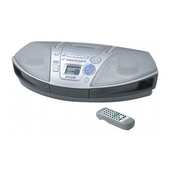
- Page 8 6. Caution for AC Mains Lead 7. Location of Controls...
- Page 9 8. The Remote Control...
- Page 10 9. Self Diagnostic Function 9.1. Setting of self-diagnosis Function 9.1.1. Setting of CD self-diagnosis mode / 1. Remove the cassette from the deck. 2. Switch to CD function. 3. Press the CD/TAPE STOP key of the main set for more than 2 seconds.
- Page 11 shall be checked and confirmed at this stage by the software. Press FF key to proceed the self-diagnosis. The FF operation shall stop automatically after 3 sec. If abnormal operation is detected, the tape shall stop automatically after 1 sec. During the FF operation, the Reel Pulse shall be checked by the software.
- Page 12 Display Symtom or condition Cause and method of correction Code When operating on batteries, power goes off The batteries are depleted. Replace with *U01 immediately after being turned on. batteries. Power cannot be switch on. The power cord (AC) or insert fresh batteries. *U02 Cassette deck does not operate correctly.
- Page 13 Some chassis components maybe have sharp edges. Be careful when diassembling and servicing. 1. This section describes the procedures for checking the operation of the major printed circuit boards and replacing the main components. 2. For assembly after operation checks or replacement, reverse trhe respective procedures.
- Page 14 10.1.1. Checking for the Panel P.C.B. Step 2: Use a screw driver and insert into the hole. Slide the screw driver to the direction shown to open the cassette lid. Step 3: Remove the two screws and lift up the front cabinet.
- Page 15 Step 5: Remove the FFC wire from CS601 and remove the front cabinet together with the Panel P.C.B. 10.1.2. Checking for Main & CD Servo P.C.B. Step 2: Remove the connector CP1450 from the Main P.C.B. Step 4: Take out the mecha chasis according to the direction shown. Step 5: Remove the FFC wire from CS801.
- Page 16 Step 6: Remove the FFC wire from CP802. Step 7: Remove the FFC wire from CS601. Step 8: Remove the wire from CP501 which is mounted on transformer P.C.B. Take out the Main P.C.B. 10.2. Disassembly and Assembly of Traverse Deck Step 1: Press down both catches on both side as shown.
- Page 17 Step 4: Remove the clamp plate and tray in sequence. Step 5: Push the cam gear drive to about 30 anticlockwise. Shift the spring away from the traverse.
- Page 18 Step 6: Press on the catch on both sides one at a time. While pressing, shift the traverse up in the manner of left to right. Step 7: Take out the traverse in a slanting manner. Note: 1. Follow the reverse procedure to replace the CD Traverse Unit and CD Tray.
- Page 19 Note: When replacing the CD Tray, make sure the dented line is at position as shown. 10.3. Main Component Replacement Procedures Step 1: Desolder 2 terminals of the traverse motor. Step 2: Desolder 2 terminals of the spindle motor. Step 3: Remove the flexible cable from CN701. - Removal of the flexible cable.
- Page 20 out the flexible cable in the direction of arrow 2. Step 4: Push the lever in and turn the gear clock wise fully. Step 6: Release the claw and remove the Driver Plate.
- Page 21 Step 7: Slide out the Optical Pick-up Unit from the indent opening. Step 8: Do not touch the lense on the OPU. 11. Schematic Diagram (All schematic diagrams may be modified at any time with the development of new technology.) Notes:...
- Page 22 S601 : FF SWITCH S602 : REW SWITCH S603 : TAPE/CD STOP SWITCH S604 : POWER SWITCH S605 : GEQ SWITCH S606 : VOLUME DECREASE SWITCH S607 : VOLUME INCREASE SWITCH S621 : CD OPEN/CLOSE SWITCH S622 : MEMORY SWITCH S623 : CLOCK/TIMER SWITCH S624 :...
- Page 23 Secondary trouble can be prevented by taking care during repair. - Cover the parts boxes made of plastics with aluminium foil. - Put a conductive mat on the work table. - Ground the soldering iron. - Do not touch the pins of IC, LSI or VLSI with fingers directly. 12.
- Page 24 14. Troubleshooting Guide...
- Page 25 15. Measurements and Adjustments 15.1. Tuner Section...
- Page 26 READ CAREFULLY BEFORE ATTEMPTING ALIGNMENT 1. Set selector switch to AM or TAPE. 2. Set volume level to 40. 3. Output of signal generator should be no higher than necessary to obtain an output reading. - AM-RF ALIGNMENT Signal Generator or Sweep Generator Radio Dial Indicator Remarks...
- Page 27 Test Tape Indicator (Electronic Adjustment Remarks Voltmeter or oscilloscope) QZZCFM Headphone Jack (32 Azimuth Screw 1. Insert a test tape (QZZFCM) and start playback )Fabricate the plug forward direction. (8 kHz, -20 (Shown in Fig. as shown in Fig. 2 2.
- Page 28 Bias voltage for Deck (Standard value): 17.3 ± 1mV (Normal) - BIAS FREQUENCY ADJUSTMENT 1. Set the unit to “TUNER MODE” position. 2. Insert the Normal blank tape (QZZCRA) into DECK and set the unit to “REC” mode (use “ REC / STOP”...
- Page 29 16. Type Illustration of IC’s, Transistors and Diodes 17. Terminal Function Of IC’s - IC701 (AN8885SBE1) Servo Amplifier...
- Page 30 Pin No. Mark Function Tracking signal input 1 Tracking signal input 2 Power supply Focus signal input terminal 1 Focus signal input terminal 2 APC amp input APC amp output RFsumming output RFIN Detector’s input CSBRT Capacitor for OFTR connection Capacitor for HPF amp connection BDO output (“H”...
- Page 31 Mark Function BCLK O N.C. LRCK O N.C. SRDATA O N.C. DVDD1 I Power supply input (for digital circuit) DVSS1 I GND (for digital circuit) O Digital audio interface signal output (Latches data at first transition) MCLK I Microprocessor command clock signal input MDATA I Microprocessor command...
- Page 33 Mark Function O Spindle motor drive signal output (forced mode output) O Spindle motor drive signal output (servo error signal output) KICK O N.C. O Traverse drive output O Focus drive output VREF I D/A (drive) output (TVD,ECS,TRD,FOD,FBAL,TBAL) Reference voltage input FBAL O Focus balance adjustment output...
- Page 34 Mark Function AVSS2 I GND (for analog circuit). O EFM signal output O PLL extraction clock output (fPCK = 4.321 MHz during normal playback) VCOF2 I/O VCO loop filter for 33.8688 MHz conversation terminal for 16.9344 MHz crystal mode, must use other circuit SUBC O Sub-code serial data output SBCK...
- Page 35 Mark Function OUTR O Right channel audio signal output RSEL I RF signal polarity assignment input (at “H” level, RSEL=”H”, at “L” level, RSEL=”L”) IOVOD I 5V supply input PSEL I Test terminal (connected to Gnd) MSEL I SMCK oscillating frequency designation input(“L”: 4.2336MHz, “H”:8.4672MHz) SSEL...
- Page 36 Mark Function O Motor driver (4) reverse - action output O Motor driver (4) forward - action output PVCC2 I Power supply (2) for driver - GND (CH2,CH3.CH4) - Not used - Not used - Not used - Not used I Power supply terminal BIAS I Bias amplifier input...
- Page 37 Mark Function PDET Power supply voltage detect ADL_IN Deck mechanism condition input VREF+ O +5 reference for A/D O No connection SUBQ I CD subcode data input SQCK O CD subcode data clock MBP1 O Micro-P beat proof control output 1 MBP2 O Micro-P beat proof control output 2...
- Page 38 Mark Function CD_RESET O CD RST output RESET_SW I CD limit SW input for the most inner point CD_OPEN O CD open input CD_CLOSE O CD close input PCNT O Power control output REM_STBY I Remote standby AI_JOG1 I AI JOG input 1 AI_JOG2 I AI JOG input 2 EDATA...
- Page 39 otherwise, P=Pico-farads (pF), F=Farads. - Resistance value are in ohms, unless specified otherwise, 1K= 1,000 (OHM). - The marking (RTL) indicates that the Retention Time is limited for this item. After the discontinuation of this assembly in production, the item will continue to be available for a specific period of time. The retention period of availability is dependent on the type of assembly, and in accordance with the laws govening part and product retention.
- Page 40 18.1.2. Deck Mechanism Parts List...
- Page 41 Ref. No. Part No. Part Name & Description Remarks CASSETTE DECK RED0062 HEAD BLOCK UNIT RDG0300 REEL BASE GEAR RDG0301 WINDING RELAY GEAR RDK0026 MAIN GEAR RDV0033-4 WINDING BELT RDV0064 CAPSTAN BELT RMB0312 TRIGGER LEVER SPRING RMB0400 REEL SPRING RMB0403 HEAB PANEL SPRING RMB0404 BRAKE ROD SPRING...
- Page 42 18.2.2. CD Loading Mechanism Parts List...
- Page 43 Ref. No. Part No. Part Name & Description Remarks TRAVERSE DECK RAE0155Z-1V CT100W TRAVERSE RDG0455 TRAVERSE GEAR (A) RDG0456 TRAVERSE GEAR (B) RFKNCT100 TRAVERSE BASE ASS’Y 304-1 RDG0457 LOAD GEAR (A) 304-10 RXQ0632 TRV MOTOR UNIT 304-2 RDG0458 LOAD GEAR (B) 304-3 RDG0459 LOAD GEAR (C)
- Page 44 18.3.2. Cabinet Parts List...
- Page 45 Ref. No. Part No. Part Name & Description Remarks CABINET AND CHASSIS RFKKXES25EBS UPPER CABIENT ASS’Y RKWX0140-Q LCD PANEL RFKJXES22EBS BOTTOM CABINET ASS’Y [M]EB RKSX0036N-H BOTTOM CABINET [M]EG RKSX0036P-H BOTTOM CABINET [M]E REX0980 MAIN TO CD REXX0212 MOTOR WIRE REEX0080 CD FFC RGKX0052C-S FRONT PANEL...
- Page 46 Ref. No. Part No. Part Name & Description Remarks P.C.B. CD SERVO P.C.B. REP2807D MAIN P.C.B./POWER-ON P.C.B./BATTERY P.C.B./SENSOR P.C.B./ REPX0193G POWER P.C.B. PANEL P.C.B. REPX0195A DECK MECHANISM P.C.B. REPX0108E INTEGRATED CIRCUITS C1BA00000331 IC TUNER C1CA00000198 IC PLL IC301 C1BA00000275 IC POWER IC302 S81350HG-Z IC 5V REGULATOR...
- Page 47 Q801 KTC3199GRTA TRANSISTOR...
- Page 48 Ref. No. Part No. Part Name & Description Remarks Q802 KTC3199GRTA TRANSISTOR Q805 RVTDTC143XST TRANSISTOR Q806 RVTDTC143XST TRANSISTOR Q807 RVTDTC143XST TRANSISTOR Q808 B1GCCFGH0002 TRANSISTOR Q809 RVTDTC143XST TRANSISTOR Q1000 RVTDTC143XST TRANSISTOR Q1101 B1DEDQ000004 TRANSISTOR Q1102 KTC3199GRTA TRANSISTOR Q1103 B1DEDQ000004 TRANSISTOR Q1104 B1DEDQ000004 TRANSISTOR Q1201...
- Page 49 Ref. No. Part No. Part Name & Description Remarks D801 B0AACK000004 DIODE D802 B0AACK000004 DIODE D803 B0AACK000004 DIODE D951 MA165TA DIODE D1500 B0BA6R100003 DIODE SWITCHES S601 EVQ21405RJ SW FF S602 EVQ21405RJ SW REW S603 EVQ21405RJ SW TAPE/CD STOP S604 EVQ21405RJ SW POWER S605 EVQ21405RJ...
- Page 50 Ref. No. Part No. Part Name & Description Remarks G0C101KA0029 AXIAL COIL RLQY30S1W FM COIL L501 RLL500050T-Y RF CHOKE COIL L502 RLL500050T-Y RF CHOKE COIL L801 G0C2R2KA0029 COIL L802 G0C2R2KA0029 COIL L811 G0C2R2KA0029 COIL L823 G0C2R2KA0029 COIL L831 G0C2R2KA0029 COIL L1301 RL09B17-T REC BIAS OSC COIL...
- Page 51 Ref. No. Part No. Part Name & Description Remarks JACKS JK301 K2HC103B0049 JK HEAD PHONE JK501 RJJ1SE01-1H JK AC INLET (SW501) WIRES W501 REXX0214 MAIN TO POWER WIRE W502 RWJ0104170SQ POWER TO BATTERY WIR W601 RWJ1110150XX WIRE W602 RWJ4202205KX MAIN TO SP.RIGHT W603 RWJ6902170KX MAIN TO SP.LEFT...
- Page 52 Ref. No. Part No. Part Name & Description Remarks R111 ERDS2TJ103T 10K 1/4W R112 ERDS2TJ822T 8.2K 1/4W R113 ERDS2TJ682T 6.8K 1/4W R115 ERDS2TJ222T 2.2K 1/4W R116 ERDS2TJ221T 220 1/4W R117 ERDS2TJ181T 180 1/4W R118 ERDS2TJ103T 10K 1/4W R119 ERDS2TJ562T 5.6K 1/4W R120 ERDS2TJ681T 680 1/4W...
- Page 53 Ref. No. Part No. Part Name & Description Remarks R320 ERDS2TJ223T 22K 1/4W R321 ERDS2TJ153T 15K 1/4W R322 ERDS2TJ1R5T 1.5 1/4W R323 ERDS2TJ1R5T 1.5 1/4W R324 ERDS2TJ1R5T 1.5 1/4W R325 ERDS2TJ471T 470 1/4W R326 ERDS2TJ471T 470 1/4W R327 ERDS2TJ101T 100 1/4W R328 ERDS2TJ331T 330 1/4W...
- Page 54 Ref. No. Part No. Part Name & Description Remarks R705 ERJ3GEYJ154V 150K 1/16W R706 ERJ3GEYJ102V 1K 1/16W R707 ERJ3GEYJ393V 39K 1/16W R708 ERJ3GEYJ223V 22K 1/16W R709 ERJ3GEYJ473V 47K 1/16W R711 ERJ3GEYJ823V 82K 1/16W R712 ERJ3GEYJ221V 220 1/16W R714 ERJ3GEY0R00V 0 1/16W R715 ERJ3GEYJ102V 1K 1/16W...
- Page 55 Ref. No. Part No. Part Name & Description Remarks R832 ERDS2TJ103T 10K 1/4W R833 ERDS2TJ103T 10K 1/4W R841 ERDS2TJ103T 10K 1/4W R842 ERDS2TJ102T 1K 1/4W R848 ERDS2TJ104T 100K 1/4W R849 ERDS2TJ104T 100K 1/4W R850 ERDS2TJ104T 100K 1/4W R855 ERDS2TJ472T 4.7K 1/4W R856 ERDS2TJ472T 4.7K 1/4W...
- Page 56 Ref. No. Part No. Part Name & Description Remarks R1310 ERDS2TJ102T 1K 1/4W R1311 ERDS2TJ563T 56K 1/4W R1313 ERDS2TJ221T 220 1/4W R1314 ERDS2TJ100T 10 1/4W R1340 ERDS2TJ223T 22K 1/4W R1341 ERDS2TJ471T 470 1/4W R1352 ERDS2TJ104T 100K 1/4W R1353 ERDS2TJ474T 470K 1/4W R1401 ERDS2TJ334T 330K 1/4W...
- Page 57 Ref. No. Part No. Part Name & Description Remarks F1D1H102A012 1000P 50V F1D1H102A012 1000P 50V F1D1H102A012 1000P 50V ECA1CAK101XB 100 16V ECA1CAK101XB 100 16V F1D1C103A004 0.01 16V F1D1H120A015 12P 50V ECBT1C222KR5 2200P 16V ECBT1H180JC5 18P 50V F1D1H101A012 100P 50V ECA1HAK2R2XB 2.2 50V F1D1H102A012 1000P 50V...
- Page 58 Ref. No. Part No. Part Name & Description Remarks C214 ECA1CAK470XB 47 16V C215 ECA1HAK3R3XB 3.3 50V C216 F1D1H333A012 0.033 50V C217 ECA1HAKR33XB 0.33 50V C218 F1D1H102A012 1000P 50V C219 ECA1CAM331XB 330 16V C220 ECFR1C223KR 0.022 16V C221 ECFR1C153KR 0.015 16V C222 F1D1H471A012 470P 50V...
- Page 59 Ref. No. Part No. Part Name & Description Remarks C722 ECUV1H100JCV 10P 50V C723 ECEA1AKA221I 220 10V C724 ECUV1C104KBV 0.1 16V C725 ECJ1VB1H102K 1000P 50V C726 ECJ1VB1H102K 1000P 50V C727 ECA1HAK010XI 1 50V C728 ECA1HAK010XI 1 50V C730 ECUV1E104ZFV 0.1 25V C731 ECA0JAK221XI 220 6.3V...
- Page 60 Ref. No. Part No. Part Name & Description Remarks C852 F1D1H102A012 1000P 50V C853 F1D1H102A012 1000P 50V C854 F1D1H101A012 100P 50V C855 F1D1H101A012 100P 50V C856 F1D1H101A012 100P 50V C865 F1D1H561A012 560P 50V C866 ECA1AAK470XB 47 10V C868 F1D1C103A004 0.01 16V C1001 ECA1CAK470XB 47 16V...
- Page 61 Ref. No. Part No. Part Name & Description Remarks RJ716 ERJ3GEY0R00V 0 1/16W RJ722 ERJ3GEY0R00V 0 1/16W RJ723 ERJ3GEY0R00V 0 1/16W RJ724 ERJ3GEY0R00V 0 1/16W RJ726 ERJ3GEY0R00V 0 1/16W RJ727 ERJ3GEY0R00V 0 1/16W RJ728 ERJ3GEY0R00V 0 1/16W RJ731 ERJ3GEY0R00V 0 1/16W RJ732 ERJ3GEY0R00V 0 1/16W...
- Page 62 Printed in Singapore / M020100001 FLE/C/E/J/S/N...
- Page 63 CD SERVO P.C.B (REP2807D) (RF) TJ701 C727 X701 TJ701 TP19 C725 R714 C716 C726 TP16 C721 C717 C728 R709 TP17 C702 TP26 C722 C744 R712 TP24 C723 C724 TP18 TP35 TP25 TP13 IC701 R721 TP27 TP14 J723 J703 C730 C732 TP11 C711 J726...
- Page 64 SCHEMATIC DIAGRAM -1 CD SERVO CIRCUIT : +B SIGNAL LINE : CD SIGNAL LINE R701 OPTICAL PICKUP CIRCUIT C701 Q701 6.3V33 3.2V 2SA1037AKSTX C703 LASER DIODE Q701 6.3V100 LASER POWER DRIVE CN701 2.7V ((2.3V)) 0.9V ((2V)) C704 R754 LD GND NBOUT C707 C714...
- Page 65 SCHEMATIC DIAGRAM - 2 CD SERVO CIRCUIT : +B SIGNAL LINE : CD SIGNAL LINE D750 MAZ80560ML R717 C727 50V1 C725 1000P R721 C726 1000P R718 C728 50V1 R761 C731 4.7K 6.3V220 CN702 Lch OUT C730 C733 C732 A.GND 6.3V220 C754 Rch OUT 470P...
- Page 66 SCHEMATIC DIAGRAM-6 : PLAYBACK SIGNAL LINE MAIN (DECK) CIRCUIT : +B SIGNAL LINE : +B SIGNAL LINE Q1103, 1104 C1107 50V1 B1DEDQ000004 C1108 R1108 HEAD SELECT 820P 3.9K R1109 (REC: ON) R1103 C1502 3.9K Q1104 16V10 R1110 C1110 C1106 R1112 RECORD/PLAY 470K 820P...
- Page 67 SCHEMATIC DIAGRAM-7 : PLAYBACK SIGNAL LINE MAIN (DECK) CIRCUIT : +B SIGNAL LINE : +B SIGNAL LINE Q1101, 1201 B1DEDQ000004 SWITCH R1204 R1104 Q1201 Q1101 R1002 4.7K Q1000 RVTDTC143XST SWITCH Q1000 Q1102 R1207 Q1202 REC_R Q1102, 1202 R1299 KTC3199GRTA REC_L SWITCH PB_R R1107...
- Page 68 SCHEMATIC DIAGRAM-3 : +B SIGNAL LINE : CD SIGNAL LINE : PLAYBACK SIGNAL LINE MAIN CIRCUIT : MAIN SIGNAL LINE : FM/AM SIGNAL LINE : RECORD SIGNAL LINE L801 G0C2R2KA0029 R803 R802 R801 150K 150K 150K C802 C803 C801 16V10 0.01 L802 G0C2R2KA0029...
- Page 69 Z801 A2ZZ00000034 COM3 SEG26 COM2 SEG27 COM1 SEG28 COM0 SEG29 VLC3 SEG30 VLC2 SEG31 VLC1 CD OPEN_SLOW OSC2 CD CLOSE_SLOW OSC1 IC801 ECLK MN101C38ABB EDATA MICON AI_JOG2 MMOD AI_JOG1 VREF- REM_STBY KEY1 PCNT KEY2 D802 R842 REG1 CD CLOSE_FIRST R841 REG2 CD OPEN_FIRST D803...
- Page 70 C851 00034 1000P C852 1000P CD L AGND CD R CD3.3V 3.3V LDSW/CLDCK C853 CD7.5V 1000P DGND CD7.5V C850 C849 220P 220P PWRGND Q808 CD SERVO CIRCUIT R893 4.7K Q808 MCLK MCLK (CN702) ON B1GCCFGH0002 R892 4.7K MDATA MDATA SCHEMATIC CD OPEN SWITCH DIAGRAM-2 R891 4.7K...
- Page 71 R101 RECR RECR 2.2K RECL RECL (2A) R119 R405 5.6K R104 1.5K DMT_L DMT_L R406 MAIN (DECK) RECH RECH C411 CIRCUIT 16V47 (2B) ON R401 C104 SCHEMATIC 50V1 DIAGRAM-7 C420 VREF- 220P R108 VREF- ADL_IN ADL_IN PHOTO PHOTO PL_H PL_H IC304 IC304 MOTOR_H...
- Page 72 R120 R220 C219 D201 B0BA7R500006 16V330 C119 D101 R215 16V330 B0BA7R500006 2.2K R111 R110 C107 C106 R123 16V10 0.056 Q101 R108 C120 C121 R121 0.022 0.015 4.7K R109 Q401 C108 SW_VCC B1DEDQ000004 R408 100P R122 C122 Q102 4.7K 470P SWITCHING R112 8.2K C123...
- Page 73 C213 Q103, 203 10V2200 2SD1450RSTA SWITCH C211 50V1 R215 2.2K R115 2.2K R302 Q203 Q103 2.7K HEADPHONE C115 C215 50V3.3 50V3.3 JK301 R303 Q318 KTC3199GRTA SWITCH Q318 R301 C304 C301 16V22 25V3300 R342 D313 B0AACK000004 R501 ACST F501 250V T4A H501/ CP501 FH501 FH502...
- Page 74 SCHEMATIC DIAGRAM - 4 : FM/AM SIGNAL LINE : AM SIGNAL LINE MAIN (TUNER) CIRCUIT : FM OSC SIGNAL LINE : +B SIGNAL LINE : AM OSC SIGNAL LINE 0.022 1000P RLV2C045-0 RL02B131-T 330P TELESCOPIC ANTENNA KV1520NT1-2 50V1 100K 100K 100K 3.3K 1000P...
- Page 75 SCHEMATIC DIAGRAM - 5 : FM/AM SIGNAL LINE MAIN (TUNER) CIRCUIT : +B SIGNAL LINE 100P 1000P 330P C1CA00000198 RSXD7M20C01 PLL IC 0.01 1000P 1000P 2.2K 50V2.2 4.7K RLQZPR22KT-Y 2200P 0.01 G0C101KA0029 3.3K Q3, Q4 2SJ498CTA 1000P 1000P 1000P 16V100 1000P 16V100 330P...
- Page 76 MAIN P.C.B ( REPX0193G SPEAKERS R327 R116 R339 R118 J183 C115 D314 C314 R117 D308 IC301 JK301 B C E 2 3 4 5 6 7 8 C315 C114 Q308 D311 J413 R335 Q313 J182 TP23 Q314 R314 Q203 Q305 TP21 FP301 R337...
- Page 77 TELESCOPIC ANTENNA R339 C315 D311 R335 Q314 R337 R336 3 4 5 R338 Q315 R306 D301 C309 Q301 1 2 3 C308 J260 J203 J173 J171 Q1454 J259 J258 J257 J105 J103 J164 J163 J159 C1451 CP1450 R1451 Q318 R553 Q551 R554 R555...
- Page 78 PANEL P.C.B (REPX0195A) S624 TIMER PLAY/REC R624 S630 CLOCK/ S629 R625 TIMER S627 S628 S625 R627 R629 R630 R626 R628 CD REC MODE DECK S626 TAPE S622 TUNER/BAND MEMORY/ CLEAR R605 R623 S603 R622 S602 S605 S601 TAPE/CD REW/ R604 C602 S604 POWER...
- Page 79 POWER-ON P.C.B BATTERY P.C.B REPX0193G REPX0193G 12V (D-TYPE, UM-1, 1.5V X 8 BATTERIES) J551 W801 J552 SENSOR P.C.B W502 REPX0193G J553 J554 SENSOR Z861 C865 C866 W802 J556 J555 6V ( AA-TYPE 1.5V X 4 BATTERIES) POWER P.C.B ( REPX0193G CP501 J501 F501 T4AL...
Need help?
Do you have a question about the RX-ES22E and is the answer not in the manual?
Questions and answers