Advertisement
Quick Links
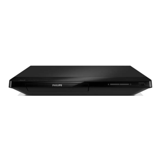
Blu-ray Player
Service
Service Manual
. Location of PCB Boards,Version Variation and Repair Scenario Matrix.....1-2
. Technical Specifications.........................................................1- 3
. Safety Instruction, Warning & Notes........................................1- 4
. DFU Instruction..............................................................................2-1
. Mechanical and Dismantling Instructions....................................3-1
. Software Upgrades .......................................................................
. Trouble Shooting Chart......................................................
. Wiring Diagram..................................................................6-1
. Electrical Diagrams and Print-layouts......................................7-1
. Votages and Waveforms for Connection Pins...........................8-1
. Pin Description & Block Diagrams of ICs..................................9-1
. Set Mechanical Exploded view & Part list...............................10-1
. Revision List.................................................................................11-1
©Copyright 2011 Philips Consumer Electronics B.V. Eindhoven, The Netherlands
All rights reserved. No part of this publication may be reproduced, stored in aretrieval system or
transmitted, in any form or by any means, electronic, mechanical, photocopying, or otherwise
without the prior permission of Philips.
Published by Arya & Sophie - 1304 BU AVM Printed in The Netherlands Subject to modification
Version 1.0
TABLE OF CONTENTS
BDP2100/12/05/F7
Page
4-1
.
5-1
.
CLASS 1
LASER PRODUCT
3141 785 39120
GB
PHILIPS
Advertisement

Related Manuals for Philips BDP2100/12/05/F7


Summary of Contents for Philips BDP2100/12/05/F7
-
Page 1: Table Of Contents
. Set Mechanical Exploded view & Part list.…………………..….…10-1 . Revision List.................11-1 CLASS 1 ©Copyright 2011 Philips Consumer Electronics B.V. Eindhoven, The Netherlands All rights reserved. No part of this publication may be reproduced, stored in aretrieval system or LASER PRODUCT transmitted, in any form or by any means, electronic, mechanical, photocopying, or otherwise without the prior permission of Philips. - Page 2 PCB BOARD LOCATIONS Main Board Loader Power Board Front Board VERSION VARIATIONS Type / Versions BDP2100 Service Policy Board in used MAIN BOARD FRONT BOARD LOADER POWER BOARD C -- Component Lever Repair Tips: * M -- Module Lever Repair X -- Used...
- Page 3 BDP2100/12/05: Specifications HDMI output Sampling frequency: MP3: 32 kHz, 44.1 kHz, 48 kHz WMA: 44.1 kHz, 48 kHz Note Constant bit rate: MP3: 112 kbps - 320 kpbs WMA: 48 kpbs - 192 kpbs Region code Compatibility: Hi-Speed USB (2.0) This player can play discs with the following Class support: USB Mass Storage Class region codes.
- Page 4 BDP2100/F7 Specifications Note Main unit Region code Accessories supplied Playable media File format Video Audio...
-
Page 5: Safety Instruction, Warning & Notes
Safety instruction, Warning & Notes Safety instruction 1. General safety 2.Laser safety Safety regulations require that during a repair: This unit employs a laser. Only qualified service personnel . Connect the unit to the mains via an isolation transformer. may remove the cover, or attempt to service this device . - Page 6 Warning 1.General 2. Laser . All ICs and many other semiconductors are susceptible to . The use of optical instruments with this product, will electrostatic discharges (ESD). Careless handing during increase eye hazard. repair can reduce life drastically. Make sure that, during .
- Page 7 Solder Joint...
- Page 8 - lead free BGA-ICs will be delivered in so-called respected by the workshop during a repair: ‘dry-packaging’ (sealed pack including a silica gel Use only lead-free solder alloy Philips SAC305 with pack) to protect the IC against moisture. After order code 0622 149 00106. If lead-free solder-paste is...
-
Page 9: Dfu Instruction
DFU Instrution Before you connect this Blu-ray disc/ DVD player, read and understand all accompanying instructions. - Page 10 Register your product and get support at www.philips.com/welcome BDP3480 BDP3480 PC & Mac EN User manual VIDEO VIDEO HDMI OUT COAXIAL COAXIAL AUDIO OUT AUDIO OUT AUDIO OUT...
- Page 11 1 HDMI HDMI VIDEO COAXIAL AUDIO LINE OUT HDMI 2 VIDEO+AUDIO LINE OUT HDMI VIDEO COAXIAL AUDIO LINE OUT AUDIO LINE OUT IO LINE VIDEO VIDEO O...
- Page 12 3 COAXIAL HDMI VIDEO COAXIAL AUDIO LINE OUT COAXIAL COAXIA A L 4 AUDIO LINE OUT HDMI VIDEO COAXIAL AUDIO LINE OUT AUDIO LINE OUT...
- Page 13 SOURCE...
- Page 14 BD 3D DVD/VCD/CD DivX Plus HD/MKV MP3 / JPEG...
- Page 15 1 Hookup and play Before you connect this Blu-ray disc/ DVD player, read and understand all accompanying instructions.
- Page 16 Use your Blu- Basic play control ray disc/ DVD player Congratulations on your purchase, and the support that Philips offers (e.g. product software upgrade), register your product at www.philips.com/welcome. During play, press the following buttons to control. Button Action Turn on the player, or switch to standby.
- Page 17 Pause play. Video options Press repeatedly to slow forward frame by frame. Start or resume play. Skip to the previous or next Fast backward or forward. Press repeatedly to change the search speed. Press once, and then press to slow forward. AUDIO Select an audio language or Access more options during video play.
- Page 18 2-10 [2D to 3D]: Convert instantly a 2D video Audio options to be viewed in 3D effect. [Picture settings] color setting. Note Available video options depend on the video source. Press repeatedly to cycle through the following options. Repeat the current track. Repeat all the tracks on the disc or folder.
- Page 19 2-11 » PIP options [1]/[2] depend on the [Cyrillic] Bulgarian, Belorussian, English, video contents. Macedonian, Moldavian, Russian, » The secondary video window is Serbian, and Ukrainian displayed. [Greek] Greek [Baltic] Northern Europe Select [2nd audio language] or [2nd Subtitle Language], and press OK. Note BD-Live on Blu-ray device, or an online video store, connect this player to a...
- Page 20 2-12 Connect this player to a computer Note network and the Internet, through wired (Ethernet) or wireless connection. BD-Live services vary from discs and countries. When you use BD-Live, data on the disc and this player For wired connection, connect a are accessed by the content provider network cable (not supplied) to the Use a USB storage device with at least 1GB of free...
- Page 21 : an online subscription service DLNA, and networking principles. If necessary, read documentation accompanying network components. streaming movies & TV episodes over the Philips is not responsible for lost, damaged, or corrupt Internet data. [YouTube]: a video-sharing service [Facebook]: a social networking service...
- Page 22 Connect this player to a home network control to control EasyLink compliant devices (see "Set up a network"). that are connected through HDMI. Philips does Connect your smartphone to the same not guarantee 100% interoperability with all home network (see the user manual of the HDMI CEC devices.
-
Page 23: Mechanical And Dismantling Instructions
Mechanical and Dismantling Instructions Dismantling Instruction Detailed information please refer to the model set. The following guidelines show how to dismantle the player. Step1: Open the top cover. Remove 2 screws on the back panel,pull back the top cover and then open it. (Figure 1) Figure 1 Step:2Remove the front panel. - Page 24 Mechanical and Dismantling Instructions Dismantling Instruction Detailed information please refer to the model set. Step3: Dismantle the power board and main board.Disconnect connectors(XP7,XP5,XP10),remove 1 screw on power board and 2 screws on the back panel.(Figure 3) Step4: Dismantle the loader.Remove 2 screws beside the loader,then pull up the loader.(FIgure 3) XP10 CN501 Figure 3...
-
Page 25: Software Upgrades
Software Upgrade Preparation to Software Upgrade 1. Procedure for software upgrade a) Upgrade from USB: 1) Go to www.philips.com/support to check if the latest software version is available for this player. 2) Build UPG_ALL file in USB 3) Copy the upgrade file to USB UPG_ALL folder. 4) Then insert USB ,start up DUT enter into HOME screen ,select Setup >>Advance>> software update >>USB. 5) When upgrade file detected, select "Yes" to upgrade, select "No" to cancel. 6) Once you start upgrade, please don’t power off the DUT, after ... - Page 26 3. Factory Reset Steps Press"Home" button on remote control‐‐‐>Press"0""3""5""8"‐‐‐> Select Restore‐‐‐>Press"OK" on remote control ...
-
Page 27: Trouble Shooting Chart
Trouble shooting chart No display on LED, and buttons do not work LED light or buttons do not work Check every supply Fix the open circuit or short circuit voltage on PSU, main which may exist on PCBs and board and front board is cables normal Check whether every pin of... - Page 28 Trouble shooting chart No audio output ( only for BDP2130 ) No audio output Check if the voltage Fix the open circuit or short on R52 and CE204 is circuit which may exist on PCBs normal Fix the RCA socket Check if the RCA socket is OK Check Fix the bad component or...
- Page 29 Trouble shooting chart Can not control by remote control Remote control does not work Check whether the remote Replace the batteries of remote control works well. control, or fix the remote control. Check whether every pin of board connects well main Fix XP1 or XP3 board, especially the 3...
- Page 30 Trouble shooting chart Can’t read disc or can’t open the disk door Can’t read disc or can’t open the disk door Check the connection of 4pin cable to the Check whether load main board or replace the loader motor motor runs well Check whether 45pin and 8pin cable from main board Fix the connection 45pin cable or...
- Page 31 Trouble shooting chart No video display No Video display Check weather the HDMI Connect the HDMI cable to the screen cable has connect to the screen Check HDMI Replace the HDMI JACK JACK is broken Replace the main board...
- Page 32 Trouble shooting chart Can not connect to network by LAN socket Can not connect to network Check weather twisted pair to Connect twisted pair Internet connect to Internet Check if the LAN socket Fix or replace and U12 is broken socket or U12 Check if the soldering and Solder or fix the abnormal...
- Page 33 Trouble shooting chart Can not connect to network by wifi Can not connect to network Check whether USB401 Fix it on main board connects wifi model well to Check if wifi circuit is OK, Fix the circuit or especially the 4 PIN in replace wifi model USB401...
- Page 34 Wiring and Block Diagram for BDP2100: NETWORK HDMI COAXIAL 01U00RJ45-403 01UHDMIIF-101 01USPDIFT-102 RESET NFLASH(256MB) 3.3V 01U0RESET-302 01UNANDFL-101 LOADER MT8551 OSC(27MHz30ppm) A CH DDR3 ASA L9830+IM422 1.5V 01UCRYSTA-502 (128MB/256MB) (ASA L9830+SANYO415 RF SIGNAL MT8560 and OTHER or SANYO416) 45PIN FFC B CH DDR3 3.3V (128MB) 1.2V...
- Page 35 Front Board Circuit Diagram: OPEN/CLOSE OPEN/CLOSE KEY1 KEY1 4PIN/2.0mm 4PIN/2.0mm USB_VCC OPEN/CLOSE R305 R305 KEY2 KEY2 USBM STANBY/ON STANBY/ON connector USBP GND1 STANBY/ON R303 R303 C313 C313 C312 C312 100pF/50V/NP0 100pF/50V/NP0 100pF/50V/NP0 100pF/50V/NP0 6PIN/2.0mm 6PIN/2.0mm OPEN/CLOSE STANBY/ON IROUT IRM_8.3mm IRM_8.3mm R328 R328 2.2K...
- Page 36 Power Board Circuit Diagram:Connector CY502 CY502 1000pF/250VAC 1000pF/250VAC L502 L502 C501 C501 R515 R515 R514 R514 R503 R503 R502 R502 1500pF/1KV 1500pF/1KV 150K 150K 150K 150K D503 D503 D501 D501 R501 R501 T501 T501 LF501 LF501 CE501 CE501 CE502 CE502 30mH 30mH CY501...
- Page 37 Power Board Circuit Diagram:Power Supply DuPont pin 14PIN/2.0mm 14PIN/2.0mm +12V +12V +12V +12V +12V IROUT IROUT IROUT IROUT IROUT USBP USBP USBP USBP USBP USBM USBM USBM USBM USBM USB_VCC USB_VCC USB_VCC USB_VCC USB_VCC VSTB VSTB VSTB VSTB VSTB VSCK VSCK VSCK VSCK...
- Page 38 Front Board Print-layout(bottom side):...
- Page 39 Power Board Print-layout(bottom side):...
- Page 40 Voltages for per connection pin XP3‐‐‐From Main Board Connect to Front Board Pin No Pin Assin Remarks 1 12V +12V 2 GND 3 IR_IN 4 VCC +5V 5 GND 6 USBP1 HIGH SPEED SIGNAL 7 USBM1 8 USB_VCC1 +5V ...
- Page 41 FUNCTIONAL BLOCK DIAGRAM FOR MANI IC MT8551 NAND DDR3 256/384MB Audio 7.1 CH 2 CH MT8551 S/PDIF Motor Driver HDMI HD+SD Decode Component 810MHz ARM11 Ethernet CVBS 400MHz AudioDSPx3 HDMI 1.4 Ethernet...
- Page 42 PIN ASSIGNMENT...
- Page 43 PIN DESCRIPTION Symbol Type Description Digital power/ground DVCC12_K Power 1.2 V digital power...
- Page 44 Symbol Type Description DGND12_K Ground Digital ground AA19 AB13 AC18...
- Page 45 Symbol Type Description DVCC33_IO Power 3.3 V digital IO power DVCC33_IO_S Power 3.3 V digital IO power for Stand-By Module DDRVCCIO Power 1.5 V digital IO power XTAL/PLL AVDD33_MEM AA21 Power 3.3 V Analog Power for MEMPLL AVSS33_MEM AB19 Ground Analog Ground for MEMPLL AA22 TN_MEMPLL...
- Page 46 Symbol Type Description Audio PWM DAC interface AVDD33_DAC Power 3.3V Analog Power AVSS33_DAC Ground Analog Ground Multiple function: (1) Audio output bit clock (2) Audio PWM output (3) GPIO Multiple function: (1) Audio output master clock (2) Audio PWM output (3) GPIO Audio interface Multiple function:...
- Page 47 Symbol Type Description Multiple function: (1) Audio output serial data 1 (2) Audio output master clock (3) Micophone input master clock (4) Video out DE signal AOSDATA1 (5) External Interrupt 1 (6) 3th RS232 TX (7) Slave I2C clock (8) PWM control signal output (9) Ethernet Activity LED (10) GPIO Multiple function:...
- Page 48 Symbol Type Description Multiple function: SPDIF (1) SPDIF digital audio output (2) GPIO Analog Video Out Interface AVDD33_VDA Power 3.3V Analog Power AVDD33_VDA Power 3.3V Analog Power AVSS33_VDAC Ground Analog Ground AVSS33_VDAC Ground Analog Ground VDACB_OUT Analog DAC output VDACG_OUT Analog DAC output VDACR_OUT...
- Page 49 Symbol Type Description Multiple function: (1) Video out 16-bit 422 mode: C0 (2) External Interrupt 4 (3) 3th RS232 RX VOUTD0 (4) Ethernet Link LED (5) NAND Flash Data input/output bit 4 (6) Secure Disk interface data bit 1 (7) GPIO Multiple function: (1) Video out 16-bit 422 mode: C1 (2) Slave I2C clock...
- Page 50 9-10 Symbol Type Description Multiple function: (1) Video out 16-bit 422 mode: C8 (2) Microphone input master clcok (3) 2nd RS232 TX VOUTD8 (4) Slave I2C clock (5) PWM control signal output (6) Ethernet Activity LED (7) NAND Flash Data input/output bit 1 (8) GPIO Multiple function: (1) Video out 16-bit 422 mode: C9...
- Page 51 9-11 Symbol Type Description Multiple function: (1) Video out 16-bit 422 mode: Y3 (2) SPDIF input bit clock (3) 2nd RS232 RX VOUTD13 I/O, 5V (4) Slave I2C data (5) External Interrupt 1 (6) Ethernet Duplex LED (7) NAND Flash command latch enable (8) GPIO Multiple function: (1) Video out 16-bit 422 mode: Y4...
- Page 52 9-12 Symbol Type Description CLK_P Analog HDMI TX clock differential pair (P) NAND Flash Interface Multiple function NFALE (1) NAND Flash address latch enable (2) GPO Multiple function NFCEN (1) NAND Flash chip enable (2) GPO Multiple function (1) NAND Flash 2 chip enable (2) 2nd RS232 TX (3) External Interrupt 2...
- Page 53 9-13 Symbol Type Description Multiple function NFD7 (1) NAND Flash Data input/output bit7 (2) GPIO Multiple function NFRBN (1) NAND Flash ready/busy (2) GPIO Multiple function (1) NAND Flash 2 ready/busy (2) 2nd RS232 RX (3) External Interrupt 1 NFRBN2 (4) 3th RS232 RX (5) Slave I2C data (6) PWM control signal output...
- Page 54 9-14 Symbol Type Description AE24 RBA1 Memory bank address bit 1 AD24 RBA2 Memory bank address bit 2 AC22 RCAS_ Memory column address strobe AE23 RCKE Memory clock enable RCLK0 Memory clock 0 positive RCLK0_ Memory clock 0 negative RCS_ Memory chip select RDQ0 Memory data bit 0...
- Page 55 9-15 Symbol Type Description RRAS_ Memory row address strobe RVREF0 Memory VREF AE25 RWE_ Memory write enable AC25 RRESET Memory reset DRAM Channel B AC10 RA0_B Memory address bit 0 RA1_B Memory address bit 1 RA2_B Memory address bit 2 AB10 RA3_B Memory address bit 3...
- Page 56 9-16 Symbol Type Description AE13 RDQ3_B Memory data bit 3 AD21 RDQ4_B Memory data bit 4 AC21 RDQ5_B Memory data bit 5 AD20 RDQ6_B Memory data bit 6 AC20 RDQ7_B Memory data bit 7 AC15 RDQ8_B Memory data bit 8 AC16 RDQ9_B Memory data bit 9...
- Page 57 9-17 Symbol Type Description Multiple function (1) Serial interface control line GPIO0 I/O, 5V (2) Slave I2C clock (3) External Interrupt 3 (4) GPIO Multiple function (1) Serial interface data line GPIO1 I/O, 5V (2) Slave I2C data (3) External Interrupt 3 (4) GPIO Multiple function (1) Video output DE signal...
- Page 58 9-18 Symbol Type Description Multiple function (1) Microphone input bit clock (2) 3th RS232 TX (3) External Interrupt 2 GPIO6 I/O, 5V (4) Slvae I2C clock (5) PWM control signal output (6) Ethernet Speed LED (7) GPIO Multiple function (1) Microphone input master clock (2) 3th RS232 RX (3) External Interrupt 4 GPIO7...
- Page 59 9-19 Symbol Type Description Reserved for debug-only Uart pins UATXD I/O, 5V (1) 1 RS232 TX (2) T8032 RS232 TX Multiple function (1) VFD clock VCLK I/O, 5V (2) GPIO (3) Slave I2C data (4) Serial interface data line Multiple function (1) VFD data VDATA I/O, 5V...
- Page 60 9-20 Symbol Type Description AVDD33_COM Power PLL/BG 3.3V analog power AVSS33_LD Ground Line driver analog ground AVSS33_PLL Ground PLL/BG analog ground AVDD12_REC Power ADC analog power AVSS12_REC Ground ADC analog ground TXVP_0 Analog Ethernet TD+ TXVP_1 Analog Ethernet RD+ TXVN_0 Analog Ethernet TD- REXT...
- Page 61 9-21 Symbol Type Description 3.3V LVTTL High frequency modulation mode selection signal output, or I/O, LDD serial interface command enable. The pin is spike-free at 5V-tolerance, power-on stage. Slow slew, FECMOD 2, 4, 6, 8mA PDR, 75K pull- down (0V) Analog Disk motor control output.
- Page 62 9-22 Symbol Type Description 3.3V LVTTL LDD serial interface data. The pin is spike-free at power-on I/O, stage. The pin is not allowed to pull-up in circuit layout. 5V-tolerance, Alternate function: FEGIO0 2,4,6,8 mA 1. Internal monitored signal output PDR, 2.
- Page 63 9-23 Symbol Type Description Read gain switch 6. The pin is not allowed to pull-up in circuit layout. Alternate function : Analog FEGIO6 1. SIDM Output 2. LCD serial interface command enable. 3. Internal monitored signal output 4. General IO. 3.3V LVTTL General IO.
- Page 64 9-24 Symbol Type Description 3.3V LVTTL High frequency modulation enable signal output, or LDD serial I/O, interface CLK or I2C SCL. The pin is spike-free at power-on 5V-tolerance, stage. Slow slew, FEOSCEN 2, 4, 6, 8mA PDR, 75K pull-up (3,3V) RFIN Differential Input of AC Coupling RF SUM Signal (Negative) Analog Input...
- Page 65 9-25 Symbol Type Description Analog Output Voltage 3 of Laser Diode Control in APC VWDC3O Output...
- Page 66 10-1 10-1 Exploded View for BDP2100/12/05:...
- Page 67 10-2 10-2 Exploded View for BDP2100/F7:...
-
Page 68: Revision List
1 1 - 1 Revision List Version 1.0 Initial Release for BDP2100/12/05 Version 1.1 Initial Release for BDP2100/F7...
Need help?
Do you have a question about the BDP2100/12/05/F7 and is the answer not in the manual?
Questions and answers