Table of Contents
Advertisement
Quick Links
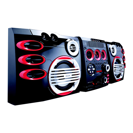
Mini System
Service
Service
Service
Service
Service
Service Manual
©
Copyright 2003 Philips Consumer Electronics B.V. Eindhoven, The Netherlands
All rights reserved. No part of this publication may be reproduced, stored in a retrieval system or
transmitted, in any form or by any means, electronic, mechanical, photocopying, or otherwise
without the prior permission of Philips.
Published by BB 0316 Service Audio
Version 1.1
TABLE OF CONTENTS
Location of pc boards & Version variations ................ 1-2
Technical Specifications ............................................. 1-3
Measurement setup .................................................... 1-4
Service Aids, Safety Instruction, etc. .......................... 1-5
Disassembly Instructions & Service positions .............. 2
Service Test Programs .................................................. 3
Set Block diagram ...................................................... 4-1
Set Wiring diagram ..................................................... 4-2
Front Control Board ....................................................... 5
Front Display Board ....................................................... 6
ECO6 Tuner Board : Systems Non-Cenelec ............. 7A
Systems Cenelec ..................... 7B
AF11 Board .................................................................... 8
P2002 110/135W Module .............................................. 9
5DTC Module (MP3 Version) ...................................... 10
Set Mechanical Exploded view & parts list ................. 11
Revision List ................................................................ 12
Printed in The Netherlands
Subject to modification
FW-M567/
Page
CLASS 1
LASER PRODUCT
GB
21/22
COMPACT
DIGITAL AUDIO
3139 785 30331
Advertisement
Chapters
Table of Contents

Related Manuals for Philips FW-M567/21


Summary of Contents for Philips FW-M567/21
- Page 1 LASER PRODUCT © Copyright 2003 Philips Consumer Electronics B.V. Eindhoven, The Netherlands All rights reserved. No part of this publication may be reproduced, stored in a retrieval system or transmitted, in any form or by any means, electronic, mechanical, photocopying, or otherwise without the prior permission of Philips.
- Page 2 LOCATION OF PRINTED CIRCUIT BOARDS MAINS SOCKET BOARD VIDEO OUT CINCH BOARD ECO POWER BOARD USB PC LINK BOARD L/R AMP. & SUPPLY BOARD USB LED BOARD IR EYE BOARD GAME PORT BOARD HEADPHONE BOARD VERSION VARIATIONS: Type /Versions: FW-M567 Features &...
- Page 3 SPECIFICATIONS GENERAL: Mains voltage : 110-127V/220-240V Switchable for /21/21M Input sensitivity Aux in (at 1kHz) : 640mV ± 2dB 120V for /37 Game Port (at 1kHz) : 310mV ± 2dB 220V for /33 220-230V for /22/34 USB (at 1kHz) : 830mV at 600 ohm 230-240V for /30 Output sensitivity Mains frequency...
- Page 4 MEASUREMENT SETUP Tuner FM Bandpass LF Voltmeter 250Hz-15kHz e.g. PM2534 e.g. 7122 707 48001 RF Generator e.g. PM5326 S/N and distortion meter e.g. Sound Technology ST1700B Use a bandpass filter to eliminate hum (50Hz, 100Hz) and disturbance from the pilottone (19kHz, 38kHz). Tuner AM (MW,LW) Bandpass LF Voltmeter...
- Page 5 SERVICE AIDS Service Tools: ESD Equipment: Universal Torx driver holder ........4822 395 91019 Anti-static table mat - large 1200x650x1.25mm ... 4822 466 10953 Torx bit T10 150mm ..........4822 395 50456 Anti-static table mat - small 600x650x1.25mm ..4822 466 10958 Torx driver set T6 - T20 .........
- Page 6 WAARSCHUWING WARNING Alle IC’s en vele andere halfgeleiders zijn All ICs and many other semi-conductors are gevoelig voor electrostatische ontladingen susceptible to electrostatic discharges (ESD). (ESD). Careless handling during repair can reduce life Onzorgvuldig behandelen tijdens reparatie kan drastically. de levensduur drastisch doen verminderen. When repairing, make sure that you are Zorg ervoor dat u tijdens reparatie via een connected with the same potential as the mass...
- Page 7 DISMANTLING INSTRUCTIONS Dismantling of the 5DTC Module Detaching the Front Panel assembly from the Bottom/Rear assembly 1) Loosen 4 screws to remove the Cover Top (pos 255) by 3) To loosen the Panel Front Display (pos 120), you have to 1) Remove 2 screws B (pos 226) as shown in Figure 5 from 2) Release the fixation of the AF Board (pos1102-A) to sliding it out towards the rear before lifting up.
- Page 8 DISMANTLING INSTRUCTIONS Dismantling of the Front Control Board and Front Display Board Dismantling of the Front Control Board and Front Display Board 1) The Knob Volume Rotary (pos 164) can be remove by 3) Loosen 4 screws D (see Figure 11) to remove the Bracket 11) Loosen 3 screws P (see Figure 14) to remove the Game 12) Loosen 2 screws Q (see Figure 15) to remove the USB pulling it out in the direction as shown in Figure 8.
- Page 9 DISMANTLING INSTRUCTIONS Dismantling of the Rear Panel assembly Dismantling of the Rear Panel assembly 1) Loosen 3 screws S and 2 catches C4 (see Figure 16) to 5) Loosen 4 screws W (see Figure 16) and 2 catches C3 remove the Tuner Board assembly. (see Figure 7) to remove the Panel Rear (pos 256) by sliding it out towards the rear (see Figure 19).
- Page 10 DISMANTLING INSTRUCTIONS Service position A Service position B Service position C...
- Page 11 SERVICE TEST PROGRAM To start service test program ™ hold & AUX depressed while plugging in the mains cord S refers to Service Mode Display shows the V refers to Version ROM version "S-Vyy" yy refers to Software version number of the uProcessor (Main menu) (counting up from 01 to 99) QUARTZ...
- Page 12 SERVICE TEST PROGRAM To start service test program ™ hold & AUX depressed while plugging in the mains cord S refers to Service Mode Display shows the V refers to Version ROM version "S-Vyy" yy refers to Software version number of the uProcessor (Main menu) (counting up from 01 to 99) 5DTC CONTROL &...
- Page 13 SET BLOCK DIAGRAM 75 ohm COAX1 (FROM 5DTC) Vpp 0.5V -VKK NOTE : -CMOS GAME -CMOS REG. MAIN SIGNAL PATH PORT MEASUREMENTS ARE IN AUX MODE : GAME 310mV LEVELS AT MAX VOL XX mV YY dBA S/N AT 500mW Game LOW_PW_SPLY ZZ dB...
- Page 14 SET WIRING DIAGRAM VU Meter Housing Left 8401 Hot Melt HR 2p/100/2p OE (37131) HR 03p/80/03p OE (37251) 1811 Video Cinch GM_RIGHT 2p EH-S Game Port HR 2P/400/2P OE Front Control 5DTC Key GND_A VIDEO OUT (37201) ( 1107-G ) CVBS (1102-B) 1803...
- Page 15 HEADPHONE BOARD - COMPONENT HEADPHONE BOARD - CHIP LAYOUT LAYOUT This assembly drawing shows a summary of all possible versions. For components This assembly drawing shows a summary of all possible versions. For components used in a specific version see schematic diagram and respective parts list. used in a specific version see schematic diagram and respective parts list.
- Page 16 CONTROL BOARD - COMPONENT LAYOUT This assembly drawing shows a summary of all possible versions. For components used in a specific version see schematic diagram and respective parts list. 3139 113 3513 pt4 dd wk0310...
- Page 17 CONTROL BOARD - CHIP LAYOUT This assembly drawing shows a summary of all possible versions. For components used in a specific version see schematic diagram and respective parts list. 3139 113 3513 pt4 dd wk0310...
- Page 18 CONTROL BOARD - CIRCUIT DIAGRAM 1600 H1 3698 E12 1602 A1 3699 E11 1603 F12 3701 F11 CONTROL 1604 B8 3702 G12 1650 F2 3703 G12 +12V_A_B +5V6 1651 E6 3704 G12 1652 E2 3705 G11 7620 # 2640 1602 2612 1653 E3 3706 H11...
- Page 19 ECO POWER BOARD - COMPONENT ECO POWER BOARD - CHIP LAYOUT GAME PORT BOARD - COMPONENT GAME PORT BOARD - CHIP LAYOUT LAYOUT LAYOUT This assembly drawing shows a summary of all possible versions. This assembly drawing shows a summary of all possible versions. This assembly drawing shows a summary of all possible versions.
- Page 20 VU METER (LEFT) BOARD - COMPONENT LAYOUT VU METER (LEFT) BOARD - CIRCUIT DIAGRAM 1810 C1 2811 D3 2814 D3 3813 D3 3816 B3 3819 B2 3822 A3 6812 A3 6815 D3 7812 B3 1811 D4 2812 C2 3811 C2 3814 D3 3817 B2 3820 B3...
- Page 21 VU METER (RIGHT) BOARD - COMPONENT LAYOUT VU METER (RIGHT) BOARD - CIRCUIT DIAGRAM 1830 C1 2831 D3 2834 D3 3833 D3 3836 B3 3839 B2 3842 A3 6830 A3 6835 D3 7832 B3 1831 D4 2832 C2 3831 C2 3834 D3 3837 B2 3840 B2...
- Page 22 IR EYE BOARD - COMPONENT LAYOUT IR EYE BOARD - CHIP LAYOUT USB LED BOARD - COMPONENT LAYOUT USB LED BOARD - CHIP LAYOUT This assembly drawing shows a summary of all possible versions. For components This assembly drawing shows a summary of all possible versions. For components This assembly drawing shows a summary of all This assembly drawing shows a summary of all used in a specific version see schematic diagram and respective parts list.
- Page 23 ELECTRICAL PARTS LIST - FRONT CONTROL BOARD ELECTRICAL PARTS LIST - FRONT CONTROL BOARD MISCELLANEOUS 1600 4822 265 11208 Flex Connector 10P 2635 2020 552 94427 100pF 5% 50V 3668 4822 117 12968 820R 5% 0,62W 3834 4822 117 12902 8k2 1% 0,063W 1602 4822 265 11535...
- Page 24 5-10 5-10 ELECTRICAL PARTS LIST - FRONT CONTROL BOARD DIODES 6881 9322 167 73676 LED VS LTL-4221NLC-KA TRANSISTORS & INTEGRATED CIRCUITS 7601 4822 209 15449 74HC4094D 7602 5322 130 60159 BC847B 7603 5322 130 60159 BC847B 7604 5322 130 60159 BC847B 7605 5322 130 60159...
- Page 25 FTD DISPLAY PIN CONNECTION FRONT DISPLAY BOARD TABLE OF CONTENTS FTD Display Pin Connection ........... 6-1 Display part - Component Layout ........6-2 ( 2G - 9G ) Display part - Chip Layout ..........6-3 Display part - Circuit Diagram ......... 6-4 5DTC Key part - Layout &...
- Page 26 DISPLAY BOARD - COMPONENT LAYOUT This assembly drawing shows a summary of all possible versions. For components used in a specific version see schematic diagram and respective parts list. 3139 113 3514 pt4 dd wk0310...
- Page 27 DISPLAY BOARD - CHIP LAYOUT This assembly drawing shows a summary of all possible versions. For components used in a specific version see schematic diagram and respective parts list. 3139 113 3514 pt4 dd wk0310...
- Page 28 DISPLAY BOARD - CIRCUIT DIAGRAM 1400 G21 1406 G1 2505 A7 2512 I2 2520 H12 2526 I17 2532 H8 2541 D17 2547 B20 2553 E19 2559 G19 2566 I7 2572 F9 2579 B9 2585 E20 3401 F10 3407 A14 3413 H18 3419 F13 3425 E14 3431 E14...
- Page 29 5DTC KEY BOARD - COMPONENT LAYOUT ELECTRICAL PARTS LIST - FRONT DISPLAY BOARD MISCELLANEOUS 1400 4822 265 11531 Flex Connector 9P 2547 4822 126 13883 220pF 5% 50V 1401 4822 265 11545 Flex Connector 19P 2548 2020 552 94427 100pF 5% 50V This assembly drawing shows a summary of all possible versions.
- Page 30 ELECTRICAL PARTS LIST - FRONT DISPLAY BOARD ELECTRICAL PARTS LIST - FRONT DISPLAY BOARD RESISTORS 3409 4822 051 30472 4k7 5% 0,062W 3463 4822 051 30102 1k 5% 0,062W 3535 4822 051 20229 22R 5% 0,1W 4407 4822 051 30008 0R Jumper 0603 3410 4822 051 20229...
- Page 31 7A-1 7A-1 BLOCK DIAGRAM TUNER BOARD ECO 6 Systems Vcc1 buffer ampl. Stab Stab Discriminator FM-RF FM-IF 1 FM-IF 2 (MPX) Vcc2 1101 Loop (1102) LF filter 10,7 MHz 10,7 MHz 10,7 MHz 1120 left left Stereo right right Det. Decoder Frontend Mixer...
- Page 32 7A-2 7A-2 1101 A1 1102 B1 1103 F2 1120 E14 1130 A2 TUNER BOARD ECO6 1131 B2 / SYSTEMS NON CENELEC 1132 G13 2101 B3 VERSION PROGRAMMING COMPONENTS 2102 B1 1101 2103 C7 2105 2104 B3 AM-IF1 1130 2105 A2 100n 5111 450kHz...
- Page 33 7A-3 7A-3 1101 A6 1120 A4 1132 A5 2128 C4 2138 C2 3142 D2 5110 B3 5114 A2 5123 D5 7112 C1 9104 B5 9107 D4 TUNER ADJUSTMENT TABLE ( ECO6 FM/MW- and FM/MW/LW - versions with AM-frame aerial ) 1102 B6 1130 B5 2106 C5...
- Page 34 7A-4 7A-4 Electrical Partslist ECO6 SYSTEMS NON CENELEC MISCELLANEOUS RESISTORS ––––––––––––––––––––––––––––––––––––––––––––––––––––– ––––––––––––––––––––––––––––––––––––––––––––––––––––– 1101 2422 015 19376 SOCKET 2P CLICKFIT 3143 © 4822 051 20223 22kΩ 0,1W USA only RDS only 1102 4822 267 10283 SOCKET COAX, IEC 75Ω 3144 © 4822 051 10102 1kΩ...
- Page 35 7B-1 7B-1 BLOCK DIAGRAM ECO6 Tuner Board SYSTEMS CENELEC version: TABLE OF CONTENTS Blockdiagram ..............7B-1 Schematic Diagram ............7B-2 Component Layout............7B-3 Adjustment table .............7B-3 Electrical Partslist ............7B-4...
- Page 36 7B-2 7B-2 1101 A2 5121 E11 1102 B1 5122 H5 1103 E2 5123 G5 1110 B2 6105-1 E4 VERSION PROGRAMMING COMPONENTS 1120 E14 6105-2 G6 TUNER BOARD ECO6 1130 A2 6106 D4 / SYSTEMS-CENELEC 1131 C2 6107 G13 VERSION AM-IF1 1132 F13 6120 C13 6120...
- Page 37 7B-3 7B-3 1101 B5 1110 B4 1131 C5 2107 B3 2133 C1 2162 A4 5102 C4 5110 A2 5114 A2 5121 B2 7104 C4 9101 A2 9104 B1 9107 B4 9110 A4 TUNER ADJUSTMENT TABLE ( ECO6 Cenelec FM/MW - and FM/MW/LW - versions with AM-frame aerial ) 1102 B5 1120 A4 1132 A4...
- Page 38 7B-4 7B-4 Electrical Partslist ECO6 SYSTEMS CENELEC MISCELLANEOUS RESISTORS DIODES ––––––––––––––––––––––––––––––––––––––––––––––––––––– ––––––––––––––––––––––––––––––––––––––––––––––––––––– ––––––––––––––––––––––––––––––––––––––––––––––––––––– 1101 2422 015 19376 SOCKET CLICKFIT 2P 3128 © 4822 117 11449 2,2kΩ 0,1W 6105 © 4822 130 83075 HN1V02H USA only LW only 1102 4822 267 10283 SOCKET COAX, IEC 75Ω...
-
Page 39: Table Of Contents
BRIEF INTRODUCTION OF THE AF11 BOARD The AF11 Board consists of the following features : a. TDA7468D IC TDA7468D IC (7501) which includes functions such as source selection, loudness control, dynamic bass control, treble control, volume control and muting function. Sound features such as ALC, DBB, DSC and IS are controllable via I C Bus from the microprocessor. -
Page 40: Af11 Board - Component Layout
AF11 BOARD - COMPONENT LAYOUT This assembly drawing shows a summary of all possible versions. For components used in a specific version see schematic diagram and respective parts list. 3139 113 3507 pt4 dd wk0310... -
Page 41: Af11 Board - Component & Chip Layout (Mapping)
AF11 BOARD - COMPONENT LAYOUT (MAPPING) AF11 BOARD - CHIP LAYOUT (MAPPING) -
Page 42: Af11 Board - Chip Layout
AF11 BOARD - CHIP LAYOUT This assembly drawing shows a summary of all possible versions. For components used in a specific version see schematic diagram and respective parts list. 3139 113 3507 pt4 dd wk0310... -
Page 43: Af11 Board - Circuit Diagram (Part 1)
AF11 BOARD - CIRCUIT DIAGRAM (PART 1) 1501 F1 3546 G8 1502 E3 3547 C9 1503 F1 3548 F8 1504 I1 3549 C9 3521 2521 1505 E4 3550 G9 TU_Left 1506 B1 3591 A10 100n 1510 F1 3592 H9 1531 C1 3593 A11 4813 1532 C2... -
Page 44: Af11 Board - Circuit Diagram (Part 2)
AF11 BOARD - CIRCUIT DIAGRAM (PART 2) 1100 F6 1201 C1 1202 E1 1203 C1 1204 E1 3412 1205 C1 1206 C1 4909 1401 A9 1402 D9 4910 4911 1401 1405 1405 A9 4.5V 1520 E6 3802 1522 A6 +5V_CD 3804 3808 1523 D6... -
Page 45: Af11 Board - Circuit Diagram (Part 3)
AF11 BOARD - CIRCUIT DIAGRAM (PART 3) 1102 H3 3671 I7 1103 H3 3672 H7 1602 F8 3673 I7 1603 E7 3674 H7 VC_OUT_LEFT 1604 A11 3675 I6 MUTE_SW_FR 2212 A10 3676 H6 3721 3722 3723 2213 A12 3677 I5 470R 2214 G5 3678 H5... - Page 46 VIDEO OUT CINCH BOARD - VIDEO OUT CINCH BOARD - CHIP ELECTRICAL PARTS LIST - AF11 BOARD COMPONENT LAYOUT LAYOUT MISCELLANEOUS 1206 4822 267 11039 Flex Connector 11P 2542 4822 124 41407 0,47uF 20% 63V 1401 4822 265 11553 Flex Connector 19P 2543 4822 126 14549 33nF 16V...
- Page 47 ELECTRICAL PARTS LIST - AF11 BOARD ELECTRICAL PARTS LIST - AF11 BOARD CAPACITORS 2928 4822 126 14043 1uF +80/-20% 16V 3534 4822 051 30273 27k 5% 0,062W 3658 4822 051 30102 1k 5% 0,062W 4146 4822 051 30008 0R Jumper 0603 2929 4822 126 14043 1uF +80/-20% 16V...
- Page 48 8-10 8-10 ELECTRICAL PARTS LIST - AF11 BOARD RESISTORS 4920 4822 051 30008 0R Jumper 0603 COILS & FILTERS 5522 4822 526 10704 FXD IND BEAD 100MHz 50R 5621 4822 156 21721 Coil 2,2uH 10% DIODES 6201 4822 130 30621 1N4148 6202 4822 130 30862...
-
Page 49: Electrical Parts List
MAINS SOCKET BOARD - COMPONENT LAYOUT This assembly drawing shows a summary of all possible versions. For components used in a specific version see schematic diagram and respective parts list. P2002 110/135W MODULE 3139 113 3482 pt2 dd wk0310 MAINS SOCKET BOARD - CIRCUIT DIAGRAM TABLE OF CONTENTS 1901 B1 5901 A2... - Page 50 MAINS BOARD - COMPONENT LAYOUT This assembly drawing shows a summary of all possible versions. For components used in a specific version see schematic diagram and respective parts list. 3139 113 3482 pt2 dd wk0310...
- Page 51 MAINS BOARD - CIRCUIT DIAGRAM 1902 A3 1912 A10 1923 A6 2902 D3 2912 F3 2924 A8 2929 B9 2934 B8 2945 D7 2953 D10 3903 E2 3912 F3 3923 B8 3953 D9 5905 B3 6903 D3 6908 D4 6916 F4 6923 C6 6928 C7 7902 E4...
- Page 52 LEFT/RIGHT AMPLIFIER & SUPPLY BOARD - COMPONENT VIEW This assembly drawing shows a summary of all possible versions. For components used in a specific version see schematic diagram and respective parts list. 3139 113 3472 pt1 dd wk0151...
- Page 53 LEFT/RIGHT AMPLIFIER & SUPPLY BOARD - CIRCUIT DIAGRAM (PART 1) 1250 A1 7242 B4 1251 A1 7250 A2 1252 F1 7251 B2 1259 A9 7252 B3 6250 1260 A9 7253 B3 3257 EH-B EH-B 1261 A9 7254 C1 1250 1251 1262 C9 7255 E1 BZX79-C15...
- Page 54 LEFT/RIGHT AMPLIFIER & SUPPLY BOARD - CIRCUIT DIAGRAM (PART 2) 1321-A C10 2322 F1 2331 B4 2340 A3 2352 A7 2364 C9 3320 C1 3327 D2 3334 A1 3342 A4 3349 F8 3356 C7 3363 C7 3370 A8 3377 F9 3393 C3 6322 E1 7320 C1...
- Page 55 LEFT/RIGHT AMPLIFIER & SUPPLY BOARD - CIRCUIT DIAGRAM (PART 3) ELECTRICAL PARTS LIST - MAINS BOARD MISCELLANEOUS 7326 A1 1925 4822 071 52502 Fuse RAD LT 2,5A 250V 5903 3103 308 30610 Transformer Standby 1926 4822 071 51602 Fuse RAD LT 1,6A 250V 5905 4822 280 10382 Relay 1P 9V 10/80A SDT-SS...
- Page 56 ELECTRICAL PARTS LIST - LEFT/RIGHT AMPLIFIER & SUPPLY BOARD ELECTRICAL PARTS LIST - LEFT/RIGHT AMPLIFIER & SUPPLY BOARD MISCELLANEOUS 0028 3139 114 73910 Holder STK PWR2002 150W 3253 4822 116 83883 470R 5% 0,5W 3343 4822 116 52291 56k 5% 0,5W 6263 4822 130 30621 1N4148...
- Page 57 10-1 5DTC Module (MP3 version) Layout stage .4 TABLE OF CONTENTS Service hints ................10-2 Location of Printed Circuit Boards ..........10-5 Wiring..................10-6 Emergency opening ..............10-7 Location of switches..............10-8 Blockdiagram ................10-9 CD B OARD Circuit Diagram ..............10-10 Component Layout side A .............10-11 Component Layout side B .............10-12 ONTROL OARD...
-
Page 58: Service Hints
10-2 Service Hints In case of symptom „skipping tracks“ perform 3. MEASURE THE EYE-PATTERN SIGNAL following actions: EYE-PATTERN SIGNAL – JITTER MEASUREMENT 1. VERIFY THE COMPLAINT Measure the signal direct on resistor 3898 using an oscilloscope (see also chapter 10-9). PLAYABILITY CHECK EYE-PATTERN Use CDDA SBC 444A: . - Page 59 10-3 Service Hints 4. MEASURE THE LASER CURRENT 6. MEASURE THE OFFSETS OF THE CD10 CD DRIVE – LASER CURRENT MEASUREMENT SIGNAL PROCESSOR – OFFSET MEASUREMENT The laser current can be measured as a voltage drop on Each ADC input of the CD10 may have an offset too. resistor 3820.
- Page 60 10-4 WARNING CHARGED CAPACITORS ON THE SERVO BOARD MAY DAMAGE THE CD DRIVE ELECTRONICS WHEN CONNECTING A NEW CDM MECHANISM. THAT´S WHY, BESIDES THE SAFETY MEASURES LIKE • SWITCH OFF POWER SUPPLY • ESD PROTECTION ADDITIONAL ACTIONS MUST BE TAKEN BY THE REPAIR TECHNICIAN. The CD drive forms a compact building block with the CD Board.
-
Page 61: Location Of Printed Circuit Boards
10-5 Location of Printed Circuit Boards CD Board MP3 Board Motor Board Control Board 5DTC Location of PCBs 2002 08 29... -
Page 62: Wiring
10-6 Wiring Diagram 5DTC Module MP3 Board Control Board 8021 Motor Board 8052 8051 1820 1825 to / from AF Board dig.out (optional) 1800 8001 CD Board 5DTC Wiring Diagram 2002 08 30 The FFC-Cables are available as sparepart. 8001 3103 308 93090 FFC CABLE 16Pin 80mm BD Connection from CD Board to CD Drive... -
Page 63: Emergency Opening
10-7 Emergency opening of the trays The trays of the 5DTC are mechanically Release snap as shown in picture 5 and pull tray out. locked. To open tray 1, 2 and 3 move lever (pos 29) backwards To remove a CD from Play Position perform following (e.g. -
Page 64: Location Of Switches
10-8 Location of switches... -
Page 65: Blockdiagram
10-9 10-9 BLOCK DIAGRAM 5DTC MP3 Version CD MECHANISM CD MAINBOARD 5,17,21,52,57 +3,3V Vref DISC 7802 1824 7887 7800 MM1469PH Vref TURNTABLE FOCB+ FOCUS CD LEFT MOTOR MOTOR Active low pass FOCB- Analog Audio Filter LM358 Vref RADB+ RADIAL CD RIGHT MOTOR RADB- SCLI... - Page 66 10-10 10-10 3912 6,1V 220R 5DTC CD BOARD 3807 3801 R2 (CD10) 7810-B 2826 3925 3873 2,4V LM358DT 3865 2851 100R LEFT LEFT CHANNEL 3926 3874 180R 2,4V 100R 3802 3808 R1 (CD10) to / from MP3 Board Active Low Pass 3803 3809 D4 (CD10)
-
Page 67: Circuit Diagram
10-11 10-11 APPING FOR APPING FOR OMPONENT AYOUT IRCUIT IAGRAM 1800 D3 3851 C5 1800 3827 1810 E5 3852 B3 1810 3828 1823 D7 3853 B6 1820 3829 1824 A5 3854 B2 1823 3831 5DTC CD Board Side A 2811 B6 3857 C1 1824 3832... - Page 68 10-12 10-12 1800 D5 1810 E3 1820 C1 1823 D1 1824 A3 1825 A4 2812 C5 2814 E4 5DTC CD Board Side B 2815 E4 2816 D4 2817 C5 2818 D4 2821 E3 2822 E3 2823 E2 2825 E2 2830 B2 2831 B4 2832 C3 2836 A6...
- Page 69 10-13 10-13 5DTC CONTROL BOARD Mapping APPING FOR IRCUIT IAGRAM 1800 3832 1802 1801 3833 1800 2810 3804 3811 3824 3833 3841 3854 3862 7805-B D3 1802 3834 1801 2811 3805 3815 3826 3834 3842 3855 3863 7806 2800 3835 3826 3863 1802...
- Page 70 10-14 10-14 MP3 B OARD IRCUIT IAGRAM MP3-CD-2002 2451 B5 2452 B2 2453 B4 2454 B7 only for FLASH version 2455 C2 2456 C12 2457 D9 2450 3465 2458 C10 100n 2459 D2 100R +3.3V +core +3.3V +3.3V 2460 E13 7458 AD16 2461 D12...
- Page 71 10-15 10-15 MP3 B OARD OMPONENT AYOUT 1460 A3 3449 C3 3460 C2 3482 B2 3492 A3 6450 C2 1451 B5 2457 A2 2469 B4 3469 C4 3479 A2 4450 A4 2456 A4 3452 B2 3461 B5 3483 B2 3493 B2 7450 B4 1455 A4 2461 D4...
- Page 72 10-16 10-16 Exploded view 5DTC mechanic - for orientation only...
-
Page 73: Mp3 Board
10-17 ELECTRICAL PARTSLIST 5DTC MODULE MP3CD Version CD Board –––––––––––––––––––––––––––––––––––––––––––––––––––––––––––––––––––––––––––––––––––––––––––––––––––––––––––––––––– MECHANICAL PARTS CAPACITORS ––––––––––––––––––––––––––––––––––––––––––––––––––––– ––––––––––––––––––––––––––––––––––––––––––––––––––––– 3103 308 54710 5DTC Module (mechanic w/o electronic) 2869 © 3198 017 34730 47nF 3103 309 05390 CD DRIVE DA12T3 2870 © 4822 126 13883 220pF 4822 529 10387 Rubber damper CD DRIVE, FRONT... - Page 74 10-18 ELECTRICAL PARTSLIST 5DTC MODULE MP3CD Version CD Board –––––––––––––––––––––––––––––––––––––––––––––––––––––––––––––––––––––––––––––––––––––––––––––––––––––––––––––––––– RESISTORS RESISTORS ––––––––––––––––––––––––––––––––––––––––––––––––––––– ––––––––––––––––––––––––––––––––––––––––––––––––––––– 3846 © 4822 051 30102 1kΩ 0,06W 3925 © 4822 051 30101 100Ω 0,06W 3847 © 4822 117 12968 820Ω 0,06W 3926 © 4822 051 30101 100Ω...
- Page 75 10-19 ELECTRICAL PARTSLIST 5DTC MODULE MP3CD Version Control Board –––––––––––––––––––––––––––––––––––––––––––––––––––––––––––––––––––––––––––––––––––––––––––––––––––––––––––––––––– MECHANICAL PARTS RESISTORS ––––––––––––––––––––––––––––––––––––––––––––––––––––– ––––––––––––––––––––––––––––––––––––––––––––––––––––– 3103 308 54710 5DTC Module (mechanic w/o electronic) 3855 © 4822 117 12706 10kΩ 0,06W 3856 © 4822 117 12706 10kΩ 0,06W MISCELLANEOUS 3857 © 4822 117 12706 10kΩ...
- Page 76 10-20 ELECTRICAL PARTSLIST 5DTC MODULE MP3CD Version MP3 Board –––––––––––––––––––––––––––––––––––––––––––––––––––––––––––––––––––––––––––––––––––––––––––––––––––––––––––––––––– MISCELLANEOUS RESISTORS ––––––––––––––––––––––––––––––––––––––––––––––––––––– ––––––––––––––––––––––––––––––––––––––––––––––––––––– 1451 2422 025 17303 FFC-CONNECTOR 19P,side entry 3484 © 4822 117 12971 15Ω 0,06W 3486 © 4822 051 30101 100Ω 0,06W CAPACITORS 3488 © 4822 117 13632 100kΩ...
- Page 77 11-1 11-1 SET MECHANICAL EXPLODED VIEW {106} [168] [167] {142} {141} {140} {143} FOR SET WITH WOOX VERSION ONLY NOT FOR ALL VERSION HOLES NOT IN ALL VERSION SHAPE VARY WITH/WITHOUT WOOX VERSION SHAPE VARY WITH/WITHOUT USB VERSION FOR FW-C7XX/M7XX ONLY { XXX } ITEM NO.
- Page 78 11-2 11-2 MECHANICAL & ACCESSORIES PARTS LIST - MAIN UNIT SCREW LISTS - MAIN UNIT 0101 3139 118 19641 Cabinet Front 0173 3139 114 78201 Cover Game Port 8410 3139 111 02501 FFC Foil 05P/180/05P AD Fold D3 x 12 0102 3139 257 50911 Panel Front 5DTC...
- Page 79 Version 1.0 (3139 785 30330) Initial Release (FW-M567/22) Version 1.1 (3139 785 30331) Introduction of FW-M567/21 Page 5-9 to 5-10 : Front Control Board - Electrical parts list adapted Page 6-5 to 6-6 : Front Display Board - Electrical parts list adapted...
Need help?
Do you have a question about the FW-M567/21 and is the answer not in the manual?
Questions and answers