LG VX8350 Service Manual
Dual band cdma (pcs/cellular/w/gps) cdma mobile phone
Hide thumbs
Also See for VX8350:
- User manual (110 pages) ,
- Quick start manual (9 pages) ,
- Specifications (2 pages)
Table of Contents
Advertisement
Quick Links
Features of VX8350
1. Wave Type
● CELLULAR : G7W
● PCS: G7W
2. Frequency Scope
Transmit Frequency (MHz)
CELLULAR
824.82 ~ 848.19
3. Rated Output Power : CELLULAR = 0.25W
4. Output Conversion Method : This is possible by correcting the key board channel.
5. Voltage and Current Value of Termination Part Amplifier (Catalogue included)
MODE
CELLULAR
PCS
6. Functions of Major Semi-Conductors
Classification
MSM6500
Memory MCP
(HYG0SEG0AF1P-6S0E)
RFR6500
RFT6150
7. Frequency Stability
● CELLULAR : ±0.5PPM
● PCS : ±0.1PPM
Copyright © 2007 LG Electronics. Inc. All right reserved.
Only for training and service purposes
PCS
1850~1910
PCS = 0.25W
Part Name
Voltage
AWT6307R
4.2V
AWT6308R
4.2V
Terminal operation control and digital signal processing
Flash Memory (512Mbit) + SDRAM (512Mbit)
Storing of terminal operation program
Converts Rx RF signal to baseband signal
Converts baseband signal to Tx RF signal
Receive Frequency (MHz)
CELLULAR
869.82~893.19
Current
Power
400mA
0.25W
400mA
0.25W
Function
PCS
GPS
1930~1990
1575.42
LGE Internal Use Only
Advertisement
Table of Contents

Related Manuals for LG VX8350


Summary of Contents for LG VX8350
- Page 1 Converts Rx RF signal to baseband signal RFT6150 Converts baseband signal to Tx RF signal 7. Frequency Stability ● CELLULAR : ±0.5PPM ● PCS : ±0.1PPM Copyright © 2007 LG Electronics. Inc. All right reserved. LGE Internal Use Only Only for training and service purposes...
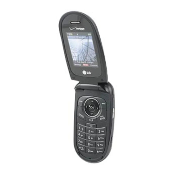
- Page 2 VX8350 Internal Use Only CDMA Mobile Subscriber Unit VX8350 SERVICE MANUAL SERVICE MANUAL DUAL BAND CDMA [PCS/Cellular/w/GPS] CDMA MOBILE PHONE Copyright © 2007 LG Electronics. Inc. All right reserved. LGE Internal Use Only Only for training and service purposes...
-
Page 3: Table Of Contents
CHAPTER 5. Safety------------------------------------------------------------------------115 CHAPTER 6. Glossary--------------------------------------------------------------------118 APPENDIX------------------------------------------------------------------------------------130 1.Assembly and Disassembly diagram-------------------------------------------------------------131 2.Block and Circuit diagram----------------------------------------------------------------------------134 3.Part List-----------------------------------------------------------------------------------------------------148 4.Component Layout--------------------------------------------------------------------------------------159 5.BGA Pin Map----------------------------------------------------------------------------------------------170 Copyright © 2007 LG Electronics. Inc. All right reserved. LGE Internal Use Only Only for training and service purposes... -
Page 4: General Introduction
Cellular uses 800MHz and PCS uses 1.9GHz. The VX8350 support GPS Mode, we usually call it tri-band phone. Also, VX8350 works on Advanced Mobile Phone Service (S-GPS). We call it dual- mode phone. If one of the Cellular, PCS base stations is located nearby, Call fail rate of triple-mode phone is less than dual-mode phone or single-mode phone. -
Page 5: Chapter 1. System Introduction
At this time, the spectrums of other signals that have different codes are not recovered into its original state, and appears as the self-interference of the system. Copyright © 2007 LG Electronics. Inc. All right reserved. LGE Internal Use Only... -
Page 6: Features And Advantages Of Cdma Mobile Phone
1.25msec (800 times per second). By doing so, the gain tolerance and the different radio propagation loss on the forward/backward link are complemented. Copyright © 2007 LG Electronics. Inc. All right reserved. LGE Internal Use Only... - Page 7 That is, each mobile station signal generates interference in relation to the signals of all the other mobile stations. Copyright © 2007 LG Electronics. Inc. All right reserved. LGE Internal Use Only...
- Page 8 Copyright © 2007 LG Electronics. Inc. All right reserved. LGE Internal Use Only...
-
Page 9: Structure And Functions Of Dual-Band Cdma Mobile Phone
Transmit signals obtained pass through the duplexer filter and then, are sent out to the cell site via the antenna. Copyright © 2007 LG Electronics. Inc. All right reserved. LGE Internal Use Only... -
Page 10: Specification
About 450 Hours (SCI=2) Standby Time About 450 Hours (SCI=2) CELLULAR 310 Minutes (-92dBm input) Talk time 310 Minutes (-92dBm input) Copyright © 2007 LG Electronics. Inc. All right reserved. LGE Internal Use Only Only for training and service purposes... - Page 11 Single Tone : -30dBm at 900 kHz (CELLULAR), -30dBm at 1.25MHz(PCS) Two Tone : -43dBm at 900 kHz & 1700kHz(CELLULAR), -43dBm at 1.25 MHz & 2.05 MHz (PCS) Copyright © 2007 LG Electronics. Inc. All right reserved. LGE Internal Use Only...
- Page 12 1851.25 1871.25 1891.25 1852.50 1872.50 1892.50 1853.75 1873.75 1893.75 1855.00 1875.00 1895.00 1856.25 1876.25 1896.25 1857.50 1877.50 1897.50 1858.75 1878.75 1898.75 Copyright © 2007 LG Electronics. Inc. All right reserved. LGE Internal Use Only Only for training and service purposes...
- Page 13 1973.75 1935.00 1955.00 1975.00 1936.25 1956.25 1976.25 1937.50 1957.50 1977.50 1938.75 1958.75 1978.75 1940.00 1960.00 1000 1980.00 1941.25 1961.25 1025 1981.25 Copyright © 2007 LG Electronics. Inc. All right reserved. LGE Internal Use Only Only for training and service purposes...
- Page 14 1.4.5.4 Bluetooth mode : 2400 MHz ~ 2483.5 MHz 1.4.6 AC Adaptor : See Appendix 1.4.7 Cigar Lighter Charger : See Appendix Copyright © 2007 LG Electronics. Inc. All right reserved. LGE Internal Use Only Only for training and service purposes...
-
Page 15: Installation
Install the microphone either by clipping I onto the sunvisor (driver’s side) or by attaching it to door post (driver’s side), using a velcro adhesive tape (not included). 1.5.3.5 Cable Connections Copyright © 2007 LG Electronics. Inc. All right reserved. LGE Internal Use Only Only for training and service purposes... - Page 16 1.5.3.5.2 Antenna Cable Connection Connect the antenna coupler cable connector from the cradle to the external antenna connector. ( Antenna is not included.) Copyright © 2007 LG Electronics. Inc. All right reserved. LGE Internal Use Only Only for training and service purposes...
-
Page 17: Chpater 2. Nam Input Method
You can see the MEID/ESN number. Press softkey “OK” (Message key) to edit more NAM1 items. Press softkey “Exit” (Contacts) to exit Service Programming. Copyright © 2007 LG Electronics. Inc. All right reserved. LGE Internal Use Only Only for training and service purposes... - Page 18 You can edit the NAM1 Home SID. Press softkey “OK” (Message key) to edit more NAM1 items. Press softkey “Back” (Contacts) to edit previous NAM1 items. Copyright © 2007 LG Electronics. Inc. All right reserved. LGE Internal Use Only Only for training and service purposes...
- Page 19 You can edit Service Code. Press softkey “OK” (Message key) to edit more NAM1 items. Press softkey “Back” (Contacts) to edit previous NAM1 items. Copyright © 2007 LG Electronics. Inc. All right reserved. LGE Internal Use Only Only for training and service purposes...
- Page 20 You can edit NAM1 True IMSI MCC. Press softkey “OK” (Message key) to edit more NAM1 items. Press softkey “Back” (Contacts) to edit previous NAM1 items. Copyright © 2007 LG Electronics. Inc. All right reserved. LGE Internal Use Only Only for training and service purposes...
- Page 21 You can edit NAM1 Home SID/NID pair. Press softkey “OK” (Message key) to edit more NAM1 items. Press softkey “Back” (Contacts) to edit previous NAM1 items. Copyright © 2007 LG Electronics. Inc. All right reserved. LGE Internal Use Only Only for training and service purposes...
- Page 22 You can edit NAM1 CDMA Primary Channel B. Press softkey “OK” (Message key) to edit more NAM1 items. Press softkey “Back” (Contacts) to edit previous NAM1 items. Copyright © 2007 LG Electronics. Inc. All right reserved. LGE Internal Use Only Only for training and service purposes...
- Page 23 Press softkey “OK” (Message key) to edit more NAM1 items. Press softkey “Back” (Contacts) to edit previous NAM1 items. Press Left, Right, Up, Down key to toggle Yes/No. Copyright © 2007 LG Electronics. Inc. All right reserved. LGE Internal Use Only Only for training and service purposes...
- Page 24 You can edit NAM1 Access Overload Class. Press softkey “OK” (Message key) to edit more NAM1 items. Press softkey “Back” (Contacts) to edit previous NAM1 items. Copyright © 2007 LG Electronics. Inc. All right reserved. LGE Internal Use Only Only for training and service purposes...
- Page 25 You can edit Slot Cycle Index. Press softkey “OK” (Message key) to save Slot Cycle Index. Press softkey “Back” (Contacts) to edit previous items. Copyright © 2007 LG Electronics. Inc. All right reserved. LGE Internal Use Only Only for training and service purposes...
- Page 26 VX8350 28) Powering Down Restart. Copyright © 2007 LG Electronics. Inc. All right reserved. LGE Internal Use Only Only for training and service purposes...
-
Page 27: Chapter 3. Circuit Description
After that, the RF signal is amplified by the Power Amp in order to have enough power for radiation. Finally, the RF signal is sent out to the cell site via the antenna after going through the duplexer. Copyright © 2007 LG Electronics. Inc. All right reserved. LGE Internal Use Only... - Page 28 VX8350 [Figure 1-1] RF Block Diagram of VX8350 Copyright © 2007 LG Electronics. Inc. All right reserved. LGE Internal Use Only Only for training and service purposes...
- Page 29 It’s main function is to limit the bandwidth of spectrum reaching the LNA and mixer, attenuate receiver spurious response and suppress local oscillator energy. As a result frequency sensitivity and selectivity of mobile phone increase. The specification of VX8350 duplexer described below ; PCS duplexer...
- Page 30 The characteristics of Low Noise Amplifier (LNA) are low noise figure, high gain, high intercept point and high reverse isolation. The frequency selectivity characteristic of mobile phone is mostly determined by LNA. The specification of VX8350 GPS LNA is described below Parameter...
- Page 31 Intercept Point (IIP3) requirements of IS-98D and J-STD-018 specifications for Sensitivity, Two-Tone Inter- modulation, and Single-tone Desensitization. Operation modes and band selection are specially controlled from the Mobile Station Modem MSM6500. The specification of VX8350 Mixers is described below: Parameter Low gain High gain...
- Page 32 R and C filter in order to generate the reference frequency of 19.2 MHz and input it into the frequency synthesizer. Frequency stability depending on temperature is ±2.0 ppm. Copyright © 2007 LG Electronics. Inc. All right reserved. LGE Internal Use Only...
-
Page 33: Digital/Voice Processing Part
The power supply part is made up of circuits for generating various types of power, used for the digital/voice processing part. Copyright © 2007 LG Electronics. Inc. All right reserved. LGE Internal Use Only Only for training and service purposes... - Page 34 Then, the errors of data received from Viterbi decoder are detected and corrected. They are voice-decoded at the Vocoder in order to output digital voice data. Copyright © 2007 LG Electronics. Inc. All right reserved. LGE Internal Use Only...
- Page 35 VX8350 [Figure 2-2] Block Diagram of Digital/Voice Processing Part Copyright © 2007 LG Electronics. Inc. All right reserved. LGE Internal Use Only Only for training and service purposes...
- Page 36 MSM6500. It is also supplied stable +2.8V_LCD by Out6 in U401 for fine view angle and LCD reflects to improve the display efficiency. 3 LEDs is used to display LCD backlight. Copyright © 2007 LG Electronics. Inc. All right reserved. LGE Internal Use Only...
-
Page 37: Chapter 4. Trouble Shooting
1. Check DC Power Supply circuit 4. Check RF Signal path 2. Check VCTCXO 5. Check Rx I/Q data Redownload S/W, Cal Copyright © 2007 LG Electronics. Inc. All right reserved. LGE Internal Use Only Only for training and service purposes... - Page 38 VX8350 4.1.1.1 Checking DC Power supply circuit (PMIC) Test Point Test Point C427 C422 Circuit Diagram Circuit Diagram Copyright © 2007 LG Electronics. Inc. All right reserved. LGE Internal Use Only Only for training and service purposes...
- Page 39 VX8350 Checking Flow Checking Flow Start Check C427(TP2) +2.9V_RX0 is OK? Check C422(TP1) +2.6V_MSMP2 is OK? Copyright © 2007 LG Electronics. Inc. All right reserved. LGE Internal Use Only Only for training and service purposes...
- Page 40 VX8350 4.1.1.2 Checking VCTCXO circuit Test Point Test Point C140 R106 Circuit Diagram Circuit Diagram Copyright © 2007 LG Electronics. Inc. All right reserved. LGE Internal Use Only Only for training and service purposes...
- Page 41 VX8350 Checking Flow Checking Flow Waveform Waveform Figure 4.1.1 (a) Figure 4.1.1 (b) Copyright © 2007 LG Electronics. Inc. All right reserved. LGE Internal Use Only Only for training and service purposes...
- Page 42 VX8350 4.1.1.3 Checking Control signal Test Point Test Point U106 pin49(SBST0) pin50(SBDT0) pin51(SBCK0) Circuit Diagram Circuit Diagram Copyright © 2007 LG Electronics. Inc. All right reserved. LGE Internal Use Only Only for training and service purposes...
- Page 43 VX8350 Checking Flow Checking Flow Waveform Waveform Figure 4.1.1 (c) Figure 4.1.1 (d) Copyright © 2007 LG Electronics. Inc. All right reserved. LGE Internal Use Only Only for training and service purposes...
- Page 44 F105 Pin5 DP100. Pin3 U109,C188, C102,L103 L111, C116 L112, L118 Circuit Diagram Circuit Diagram PCS Tx DCN Tx PCS Rx DCN Rx Copyright © 2007 LG Electronics. Inc. All right reserved. LGE Internal Use Only Only for training and service purposes...
- Page 45 VX8350 Checking Flow Checking Flow Copyright © 2007 LG Electronics. Inc. All right reserved. LGE Internal Use Only Only for training and service purposes...
- Page 46 VX8350 Waveform Waveform U100 pin4 Figure 4.1.1 (e) F105 pin5 Figure 4.1.1 (f) DP100 pin3 Figure 4.1.1 (g) Copyright © 2007 LG Electronics. Inc. All right reserved. LGE Internal Use Only Only for training and service purposes...
- Page 47 4.1.1.5 Checking Rx I/Q data Test Point Test Point U106 Pin7 (RX0_QM) Pin8 (RX0_QP) Pin9 (RX0_IM) Pin10 (RX0_IP) Circuit Diagram Circuit Diagram Copyright © 2007 LG Electronics. Inc. All right reserved. LGE Internal Use Only Only for training and service purposes...
- Page 48 VX8350 Checking Flow Checking Flow Waveform Waveform RX0_QP RX0_IP RX0_Q RX0_IM RX_Q_ RX_Q_ Figure 4.1.1(h) Figure 4.1.1(i) Copyright © 2007 LG Electronics. Inc. All right reserved. LGE Internal Use Only Only for training and service purposes...
-
Page 49: Pcs
1. Check DC Power Supply circuit 4. Check RF Signal path 2. Check VCTCXO 5. Check Rx I/Q data Redownload S/W, Cal Copyright © 2007 LG Electronics. Inc. All right reserved. LGE Internal Use Only Only for training and service purposes... - Page 50 VX8350 4.1.2.1 Checking DC Power supply circuit (PMIC) Test Point Test Point C427 C422 Circuit Diagram Circuit Diagram Copyright © 2007 LG Electronics. Inc. All right reserved. LGE Internal Use Only Only for training and service purposes...
- Page 51 VX8350 Checking Flow Checking Flow Start Check C427(TP2) +2.9V_RX0 is OK? Check C422(TP1) +2.6V_MSMP2 is OK? Copyright © 2007 LG Electronics. Inc. All right reserved. LGE Internal Use Only Only for training and service purposes...
- Page 52 VX8350 4.1.2.2 Checking VCTCXO circuit Test Point Test Point C140 R106 Circuit Diagram Circuit Diagram Copyright © 2007 LG Electronics. Inc. All right reserved. LGE Internal Use Only Only for training and service purposes...
- Page 53 VX8350 Checking Flow Checking Flow Waveform Waveform Figure 4.1.2 (a) Figure 4.1.2 (b) Copyright © 2007 LG Electronics. Inc. All right reserved. LGE Internal Use Only Only for training and service purposes...
- Page 54 VX8350 4.1.2.3 Checking Control signal Test Point Test Point U106 pin49(SBST0) pin50(SBDT0) pin51(SBCK0) Circuit Diagram Circuit Diagram Copyright © 2007 LG Electronics. Inc. All right reserved. LGE Internal Use Only Only for training and service purposes...
- Page 55 VX8350 Checking Flow Checking Flow Waveform Waveform Figure 4.1.2 (c) Figure 4.1.2 (d) Copyright © 2007 LG Electronics. Inc. All right reserved. LGE Internal Use Only Only for training and service purposes...
- Page 56 F105 Pin7 U101,C187, L137,L105 DP101. Pin2 L124, C117 L113, L119 Circuit Diagram Circuit Diagram PCS Tx DCN Tx PCS Rx DCN Rx Copyright © 2007 LG Electronics. Inc. All right reserved. LGE Internal Use Only Only for training and service purposes...
- Page 57 VX8350 Checking Flow Checking Flow Copyright © 2007 LG Electronics. Inc. All right reserved. LGE Internal Use Only Only for training and service purposes...
- Page 58 VX8350 Waveform Waveform U100 Pin 4 Figure 4.1.2(e) F105 Pin 7 Figure 4.1.2(f) DP101 Pin 2 Figure 4.1.2(g) Copyright © 2007 LG Electronics. Inc. All right reserved. LGE Internal Use Only Only for training and service purposes...
- Page 59 4.1.2.5 Checking Rx I/Q data Test Point Test Point U106 Pin7 (RX0_QM) Pin8 (RX0_QP) Pin9 (RX0_IM) Pin10 (RX0_IP) Circuit Diagram Circuit Diagram Copyright © 2007 LG Electronics. Inc. All right reserved. LGE Internal Use Only Only for training and service purposes...
- Page 60 VX8350 Checking Flow Checking Flow Waveform Waveform RX0_QP RX0_IP RX0_Q RX0_IM RX_Q_ RX_Q_ Figure 4.1.2(h) Figure 4.1.2(i) Copyright © 2007 LG Electronics. Inc. All right reserved. LGE Internal Use Only Only for training and service purposes...
-
Page 61: Tx Part Trouble
1. Check DC Power Supply circuit 7. Check Triplexer 2. Check VCTCXO 8. Check Mobile Switch 3. Check RFT6150 Redownload S/W, Cal Copyright © 2007 LG Electronics. Inc. All right reserved. LGE Internal Use Only Only for training and service purposes... - Page 62 VX8350 4.2.1.1 Checking DC Power supply circuit (PMIC) Test Point Test Point C422 C424 Circuit Diagram Circuit Diagram Copyright © 2007 LG Electronics. Inc. All right reserved. LGE Internal Use Only Only for training and service purposes...
- Page 63 VX8350 Checking Flow Checking Flow Copyright © 2007 LG Electronics. Inc. All right reserved. LGE Internal Use Only Only for training and service purposes...
- Page 64 VX8350 4.2.1.2 Checking VCTCXO circuit Test Point Test Point C140 R106 Circuit Diagram Circuit Diagram Copyright © 2007 LG Electronics. Inc. All right reserved. LGE Internal Use Only Only for training and service purposes...
- Page 65 4.2.1 (b)) Replace X100 and then check R106, C140 Is it similar? Waveform Waveform Figure 4.2.1 (a) Figure 4.2.1 (b) Copyright © 2007 LG Electronics. Inc. All right reserved. LGE Internal Use Only Only for training and service purposes...
- Page 66 TX_QM PIN 28 U107 PIN 29 PIN 30 TX_IP PIN 1, 2, 3, 4 TX_IM TX_ON,SBCK0,SBDT0, SBST0 Circuit Diagram Circuit Diagram Copyright © 2007 LG Electronics. Inc. All right reserved. LGE Internal Use Only Only for training and service purposes...
- Page 67 Check pin2, 3, 4 at U107(TP5) Check SBI signal line & MSM Referring to Figure 4.2.1(f). Is it similar? Replace U107 Copyright © 2007 LG Electronics. Inc. All right reserved. LGE Internal Use Only Only for training and service purposes...
- Page 68 VX8350 Waveform Waveform Figure 4.2.1(c) Figure 4.2.1(e) RX_I_P RX_Q_P RX_Q_N RX_I_N Figure 4.2.1(d) Figure 4.2.1(f) Copyright © 2007 LG Electronics. Inc. All right reserved. LGE Internal Use Only Only for training and service purposes...
- Page 69 RF_OUT F104 RF_IN Checking Flow Waveform Checking Flow Waveform RF_IN fed up with CW signal RF_IN Figure 4.2.1(g) RF_OUT Figure 4.2.1(h) Copyright © 2007 LG Electronics. Inc. All right reserved. LGE Internal Use Only Only for training and service purposes...
- Page 70 VX8350 4.2.1.5 Check DCN PAM circuit Test Point Test Point RFOUT VMODE VBATT RFIN Circuit Diagram Circuit Diagram Copyright © 2007 LG Electronics. Inc. All right reserved. LGE Internal Use Only Only for training and service purposes...
- Page 71 Checking Flow Checking Flow Waveform Waveform RF_IN fed up with CW signal in low gain mode of PAM RF_IN RF_OUT Figure 4.2.1(i) Copyright © 2007 LG Electronics. Inc. All right reserved. LGE Internal Use Only Only for training and service purposes...
- Page 72 Circuit Diagram Test Point Circuit Diagram ANT_PORT DP100 TX_PORT Checking Flow Waveform Checking Flow Waveform Tx Port ANT Port Figure 4.2.1(j) Copyright © 2007 LG Electronics. Inc. All right reserved. LGE Internal Use Only Only for training and service purposes...
- Page 73 Test Point Circuit Diagram Ant Port F105 DCN Port Checking Flow Waveform Checking Flow Waveform DCN Port ANT Port Figure 4.2.1(k) Copyright © 2007 LG Electronics. Inc. All right reserved. LGE Internal Use Only Only for training and service purposes...
- Page 74 Circuit Diagram Test Point Circuit Diagram RF OUT RF IN Checking Flow Waveform Checking Flow Waveform RF IN RF OUT Figure 4.2.1(l) Copyright © 2007 LG Electronics. Inc. All right reserved. LGE Internal Use Only Only for training and service purposes...
-
Page 75: Pcs
1. Check DC Power Supply circuit 7. Check Triplexer 2. Check VCTCXO 8. Check Mobile Switch 3. Check RFT6150 Redownload S/W, Cal Copyright © 2007 LG Electronics. Inc. All right reserved. LGE Internal Use Only Only for training and service purposes... - Page 76 VX8350 4.2.2.1 Checking DC Power supply circuit (PMIC) Test Point Test Point C422 C424 Circuit Diagram Circuit Diagram Copyright © 2007 LG Electronics. Inc. All right reserved. LGE Internal Use Only Only for training and service purposes...
- Page 77 VX8350 Checking Flow Checking Flow Copyright © 2007 LG Electronics. Inc. All right reserved. LGE Internal Use Only Only for training and service purposes...
- Page 78 VX8350 4.2.2.2 Checking VCTCXO circuit Test Point Test Point C140 R106 Circuit Diagram Circuit Diagram Copyright © 2007 LG Electronics. Inc. All right reserved. LGE Internal Use Only Only for training and service purposes...
- Page 79 VX8350 Checking Flow Checking Flow Waveform Waveform Figure 4.2.2 (a) Figure 4.2.2 (b) Copyright © 2007 LG Electronics. Inc. All right reserved. LGE Internal Use Only Only for training and service purposes...
- Page 80 TX_QM PIN 28 U107 PIN 29 PIN 30 TX_IP PIN 1, 2, 3, 4 TX_IM TX_ON,SBCK0,SBDT0, SBST0 Circuit Diagram Circuit Diagram Copyright © 2007 LG Electronics. Inc. All right reserved. LGE Internal Use Only Only for training and service purposes...
- Page 81 Check pin2, 3, 4 at U107(TP5) Check SBI signal line & MSM Referring to Figure 4.2.2(f). Is it similar? Replace U107 Copyright © 2007 LG Electronics. Inc. All right reserved. LGE Internal Use Only Only for training and service purposes...
- Page 82 VX8350 Waveform Waveform Figure 4.2.2(c) Figure 4.2.2(e) RX_I_P RX_Q_P RX_Q_N RX_I_N Figure 4.2.2(d) Figure 4.2.2(f) Copyright © 2007 LG Electronics. Inc. All right reserved. LGE Internal Use Only Only for training and service purposes...
- Page 83 RF_OUT F103 RF_IN Checking Flow Waveform Checking Flow Waveform RF_IN fed up with CW signal RF_IN Figure 4.2.2(g) RF_OUT Figure 4.2.2(h) Copyright © 2007 LG Electronics. Inc. All right reserved. LGE Internal Use Only Only for training and service purposes...
- Page 84 VX8350 4.2.2.5 Check PCS PAM circuit Test Point Test Point RFOUT VMODE VBATT RFIN Circuit Diagram Circuit Diagram Copyright © 2007 LG Electronics. Inc. All right reserved. LGE Internal Use Only Only for training and service purposes...
- Page 85 Checking Flow Checking Flow Waveform Waveform RF_IN fed up with CW signal in low gain mode of PAM RF_OUT Figure 4.2.2(i) Copyright © 2007 LG Electronics. Inc. All right reserved. LGE Internal Use Only Only for training and service purposes...
- Page 86 Circuit Diagram Test Point Circuit Diagram ANT_PORT DP101 TX_PORT Checking Flow Waveform Checking Flow Waveform Tx Port ANT Port Figure 4.2.2(j) Copyright © 2007 LG Electronics. Inc. All right reserved. LGE Internal Use Only Only for training and service purposes...
- Page 87 Test Point Circuit Diagram Ant Port F105 PCS Port Checking Flow Waveform Checking Flow Waveform PCS Port ANT Port Figure 4.2.2(k) Copyright © 2007 LG Electronics. Inc. All right reserved. LGE Internal Use Only Only for training and service purposes...
- Page 88 Circuit Diagram Test Point Circuit Diagram RF OUT RF IN Checking Flow Waveform Checking Flow Waveform RF IN RF OUT Figure 4.2.2.9 Copyright © 2007 LG Electronics. Inc. All right reserved. LGE Internal Use Only Only for training and service purposes...
-
Page 89: Logic Part Trouble
Circuit Diagram L402 +1.4V_MSMC L403 +1.8V_MSMP1 +2.6V_MSMP2 +2.6V_MSMA U401 +2.9V_RXO +2.85V_TCXO Test point Test point +2.9V_RXO +2.85V_TCXO U401 +2.6V_MSMA +2.6V_MSMP2 +1.8V_MSMP1 +1.4V_MSMC Copyright © 2007 LG Electronics. Inc. All right reserved. LGE Internal Use Only Only for training and service purposes... - Page 90 VX8350 Checking Flow Checking Flow Copyright © 2007 LG Electronics. Inc. All right reserved. LGE Internal Use Only Only for training and service purposes...
- Page 91 4.3.1.2 Charging Trouble Circuit Diagram Circuit Diagram Battery Vcc D601 C420 C611 C410 Test point Test point U600 D601 Q600 Pin4 CON600 Copyright © 2007 LG Electronics. Inc. All right reserved. LGE Internal Use Only Only for training and service purposes...
- Page 92 Check the Battery contact pin [ CON600 ] Is the battery charged The battery may have the problem Change the battery and try again. Charging will operate properly Copyright © 2007 LG Electronics. Inc. All right reserved. LGE Internal Use Only Only for training and service purposes...
-
Page 93: Lcd
F606 F604 C428 2.8V LCD C604 Test point Test point F605 F606 F208 F207 Test point F602 F603 F604 C604 2.8V Copyright © 2007 LG Electronics. Inc. All right reserved. LGE Internal Use Only Only for training and service purposes... - Page 94 The soldering status of Replace CON603 CON603 is OK? Change the FPCB Is main FPCB good? LCD will be worked properly. Copyright © 2007 LG Electronics. Inc. All right reserved. LGE Internal Use Only Only for training and service purposes...
-
Page 95: Camera
Power 8-bit CAM_DATA line Vsync ,Hsync , SDA , Test point Test point R610(Pclk) R611(Mclk) F607 _24Mhz _19.2Mhz Camera data line Copyright © 2007 LG Electronics. Inc. All right reserved. LGE Internal Use Only Only for training and service purposes... - Page 96 VX8350 Test point Test point C439_ IOVDD R421_ AVDD R422_ DVDD Copyright © 2007 LG Electronics. Inc. All right reserved. LGE Internal Use Only Only for training and service purposes...
- Page 97 F607 looks good? Replace FPCB Check the FPCB Replace camera module & FPCB & Check the R610(24Mhz) R611 Camera will work properly Copyright © 2007 LG Electronics. Inc. All right reserved. LGE Internal Use Only Only for training and service purposes...
-
Page 98: Audio
Circuit Diagram C429 C425 VR401 VR400 VR402 C400 U400 VR403 Test points Test points VR400 VR401 C400 C425 VR402 U400 C429 VR403 Copyright © 2007 LG Electronics. Inc. All right reserved. LGE Internal Use Only Only for training and service purposes... - Page 99 Check the Soldering VR400,VR401,VR402, VR403 U400 of U400 Re-solder U400 Check the state Of contact of speaker Speaker will work properly Copyright © 2007 LG Electronics. Inc. All right reserved. LGE Internal Use Only Only for training and service purposes...
- Page 100 VX8350 4.3.4.2 Receiver Trouble Circuit Diagram Circuit Diagram C429 C401 L400 U400 L401 Test points Test points L401 L400 U400 C429 Copyright © 2007 LG Electronics. Inc. All right reserved. LGE Internal Use Only Only for training and service purposes...
- Page 101 Check the Soldering L400, L401 U400 of U400 Re-solder U400 Check the state Of contact of receiver Receiver will work properly Copyright © 2007 LG Electronics. Inc. All right reserved. LGE Internal Use Only Only for training and service purposes...
- Page 102 VX8350 4.3.4.3 MIC Trouble Circuit Diagram Circuit Diagram R203 C208 U201 C210 Copyright © 2007 LG Electronics. Inc. All right reserved. LGE Internal Use Only Only for training and service purposes...
- Page 103 VX8350 Test points Test points MIC network MSM6500 C210 C208 R203 U201 Copyright © 2007 LG Electronics. Inc. All right reserved. LGE Internal Use Only Only for training and service purposes...
- Page 104 Check the soldering of Re-solder C208,C210 C208, C210 Check the soldering Replace MIC network of MIC network MIC will work properly Copyright © 2007 LG Electronics. Inc. All right reserved. LGE Internal Use Only Only for training and service purposes...
- Page 105 VX8350 4.3.4.4 Headset Trouble Circuit Diagram Circuit Diagram PMIC(U401) 내부 Inverter R308 U401 CON301 C405 C406 Copyright © 2007 LG Electronics. Inc. All right reserved. LGE Internal Use Only Only for training and service purposes...
- Page 106 VX8350 Test points Test points PIN3 PIN2 CON301 PIN1 U401 PIN1 PIN5 PIN4 R308 C405 C406 Copyright © 2007 LG Electronics. Inc. All right reserved. LGE Internal Use Only Only for training and service purposes...
- Page 107 Headset sending Can you hear your voice Path problem from the headset? The headset will work properly Copyright © 2007 LG Electronics. Inc. All right reserved. LGE Internal Use Only Only for training and service purposes...
- Page 108 Check the Soldering of is 1.65~2.1V? R308 Re-solder R308 Check the soldering of Replace U401 U401 Level of Download S/W EAR_JACK_SENSE/ Copyright © 2007 LG Electronics. Inc. All right reserved. LGE Internal Use Only Only for training and service purposes...
- Page 109 Level of pin4 of CON301 Re-solder R308 is 1.65~2.1V? Download S/W Does it work? Change main board Does it work well? Copyright © 2007 LG Electronics. Inc. All right reserved. LGE Internal Use Only Only for training and service purposes...
-
Page 110: Backlight
R514 Main Keypad LED Enable Q500 LED Switching Tr. Test point Test point LED500 ~ LED515 R514 Main Keypad LED Enable Q600 LED Switching Tr. Copyright © 2007 LG Electronics. Inc. All right reserved. LGE Internal Use Only Only for training and service purposes... - Page 111 VX8350 Checking Flow Checking Flow Copyright © 2007 LG Electronics. Inc. All right reserved. LGE Internal Use Only Only for training and service purposes...
-
Page 112: Vibrator
4.3.6.1 Operating Vibrator Circuit Diagram Circuit Diagram U401 PMIC +3.0V_Motor CON603 B’d to B’d +3.0V_Motor Test point Test point C412 +3.0V_Motor C605 +3.0V_Motor Copyright © 2007 LG Electronics. Inc. All right reserved. LGE Internal Use Only Only for training and service purposes... - Page 113 Setting: “ON” at the motor test of “test mode” Start Is the Operating voltage of MOTOR about 3.0V Re-solder U401[PMIC] Motor will work properly Copyright © 2007 LG Electronics. Inc. All right reserved. LGE Internal Use Only Only for training and service purposes...
-
Page 114: Bluetooth Part Trouble
Circuit Diagram 4.4.2 Bluetooth Block Test Point Test Point C304 U302 Pin 14 U302 Pin 10 U302 U302 Pin 9 BT_CLK Copyright © 2007 LG Electronics. Inc. All right reserved. LGE Internal Use Only Only for training and service purposes... - Page 115 The Problem may be RF Part Similar to bellow Graph 1.2? Refer to RX Troubleshoot Replace U302 Graph 1.1 Graph 1.2 Copyright © 2007 LG Electronics. Inc. All right reserved. LGE Internal Use Only Only for training and service purposes...
-
Page 116: Chapter 5. Safety
Use only the supplied or approved antenna. Non-approved antennas, modifications, or attachments, could impair call quality, damage the phone, and violate FCC regulations. Copyright © 2007 LG Electronics. Inc. All right reserved. LGE Internal Use Only Only for training and service purposes... - Page 117 Copyright © 2007 LG Electronics. Inc. All right reserved. LGE Internal Use Only Only for training and service purposes...
- Page 118 Rule of Thumb: Using common sense at all times when handling, installing or using the phone. Any questions should be directed to you nearest Service Center or authorized service technician or electrician. Copyright © 2007 LG Electronics. Inc. All right reserved. LGE Internal Use Only...
-
Page 119: Chapter 6. Glossary
A-key. A secret, 64-bit pattern stored in the mobile station. It is used to generate update the mobile station’s Shared Secret Data. The A-key is used in the mobile station authentication process. Copyright © 2007 LG Electronics. Inc. All right reserved. LGE Internal Use Only... - Page 120 CDMA Channel. The set of channels transmitted between the base station within a given CDMA frequency assignment. See also Forward CDMA Channel and Reverse CDMA Channel. Copyright © 2007 LG Electronics. Inc. All right reserved. LGE Internal Use Only Only for training and service purposes...
- Page 121 Dim-and-Burst. A frame in which primary traffic is multiplexed with either secondary traffic or signaling traffic. Copyright © 2007 LG Electronics. Inc. All right reserved. LGE Internal Use Only...
- Page 122 Paging Channels, and up to 63 Traffic Channels, as long as the total number of channels, including the Pilot Channel, is no greater than 64. Copyright © 2007 LG Electronics. Inc. All right reserved. LGE Internal Use Only Only for training and service purposes...
- Page 123 Layer 3. Layer 3 provides the control of the Cellular telephone systems. Signaling messages originate and terminate at layer 3. See also Layering and Layer 2. Copyright © 2007 LG Electronics. Inc. All right reserved. LGE Internal Use Only Only for training and service purposes...
- Page 124 Mobile Switching Center (MSC). A configuration of equipment that provides Cellular radiotelephone service. Also called the Mobile Telephone Switching Office (MTSO) Copyright © 2007 LG Electronics. Inc. All right reserved. LGE Internal Use Only Only for training and service purposes...
- Page 125 Optional Field. A field defined within a message structure that is optionally to the message recipient. Order. A type of message that contains control codes for either the mobile station or the base station. Copyright © 2007 LG Electronics. Inc. All right reserved. LGE Internal Use Only...
- Page 126 Pilot PN Sequence Offset Index. The PN offset in units of 64 PN chips of a pilot, relative to the zero offset pilot PN sequence. Copyright © 2007 LG Electronics. Inc. All right reserved. LGE Internal Use Only Only for training and service purposes...
- Page 127 Request. A layer 3 message generated by either the mobile station or the base station to retrieve information, ask for service, or command an action. Copyright © 2007 LG Electronics. Inc. All right reserved. LGE Internal Use Only Only for training and service purposes...
- Page 128 Slotted Mode. An operation mode of the mobile station in which the mobile station monitors only selected slots on the Paging Channel when in the Mobile Station Idle State. Copyright © 2007 LG Electronics. Inc. All right reserved. LGE Internal Use Only...
- Page 129 Time Reference. A reference established by the mobile station that is synchronous with the earliest arriving multipath component used for demodulation. Copyright © 2007 LG Electronics. Inc. All right reserved. LGE Internal Use Only Only for training and service purposes...
- Page 130 Zone-Based Registration. An autonomous registration method in which the mobile station registers whenever it enters a zone that is not in the mobile station’s zone list. ㎲. Microsecond Copyright © 2007 LG Electronics. Inc. All right reserved. LGE Internal Use Only Only for training and service purposes...
-
Page 131: Appendix
VX8350 Appendix Appendix Assembly and Disassembly diagram Block and Circuit diagram Part List Component Layout BGA Pin Map Copyright © 2007 LG Electronics. Inc. All right reserved. LGE Internal Use Only Only for training and service purposes... -
Page 132: Assembly And Disassembly Diagram
1. Assembly and Disassembly Diagram... - Page 133 Internal Use Only...
- Page 134 Internal Use Only...
-
Page 135: Block And Circuit Diagram
2. Block and Circuit Diagram... - Page 136 Secondary Path Pre-LNA Rx1_Q MIDI Directly connected to F100,B7840 Video U108 MPEG-4 ALM1106-TR1 H.263, H.264 Graphics Diversity Rx OpenGL® ES 3D, 2D LO Gen GPS VCO Camera &Dist RFR6500 PLL1 VX8350 RF Part Processing Loop Filter Block Diagram for GPS...
- Page 137 2XComparator 262K Separate LDO Separate LDO 9*LDO 9*LDO RFR6500 Charger Charger 5V(600mA) 5V(600mA) RFT6150 Internal Use Only 1 2 3 1 2 3 4 5 6 4 5 6 7 8 9 7 8 9 VX8350 Logic Part Block Diagram...
- Page 138 Internal Use Only VX8350 Circuit Diagram (Main/fpcb) 1.VX8350 Main PCB (Rev1.0) 2.VX8350 sub_fpcb (Rev1.0) 3.VX8350 mod_fpcb (Rev1.2) 4.VX8350 cam_key (Rev1.0) 5.VX8350 vol_key (Rev1.0)
- Page 139 ANT100 ANT101 U105 AAT4280IJS-3-TI +2.85V_TX +2.85V_TX IN_1 +2.6V_MSMP2 R127 Internal Use Only R111 IN_2 +VPWR R104 +2.85V_TX TX_ON ON/OFF IN_3 C143 IN_5 L100 IN_4 10u-10V U102 LMV228TLX-NOPB C103 100p C191 PCS Tx RF SAW HDET_IN +2.85V_TX RFIN/EN F103 R103 B9014 1.2k B1 GND HDET_ADC...
- Page 140 [MIC NETWORK] SDRAM_CLK C216 C218 C205 Internal Use Only 100p 100p R203 MIC_BIAS U201 2.2k MIC1P OBE-415L42-RC3310LX 100n C219 C208 +1.4V_MSMC VR202 ICVL0505101V150FR C222 C225 100n +1.8V_MSMP1 C223 C227 C224 MIC1N C228 +1.8V_MSMP2_NAND C210 C206 VR200 R211 100p ICVL0505101V150FR 2.2k C211 100n SBST0...
- Page 141 Internal Use Only [HYNIX MCP] (512Mbit NAND FLASH + 512Mbit SDRAM) TP300 A[0] D1[0] A[1] D1[1] A[2] D1[2] A[3] D1[3] A[4] D1[4] A[5] D1[5] A[6] D1[6] A[7] D1[7] A[8] D1[8] A[9] D1[9] A[10] DQ10 D1[10] A[11] D1[11] DQ11 A[12] DQ12 D1[12] D2[0] I/O0...
- Page 142 Internal Use Only [PMIC] L402 [SPK CON.] MIPF2016D2R2 +1.4V_MSMC +VPWR R404 U402 130k +V_CHAR SIDEKEY_4PIN_MAIN C420 C434 2.2u 4.7u C432 1608 SPK_L_N 1608 R405 150p C419 100k SPK_L_P 100n C410 SPK_R_P SPK_R_N L403 MIPF2016D2R2 +1.8V_MSMP2_NAND R413 +1.8V_MSMP1 R406 150k C435 2.2u C433 TP401...
- Page 143 Internal Use Only [MAIN KEY] <KEY MATRIX> SW501 SW507 SW512 SW517 KYPD[9] SOFT1 SOFT2 LEFT RIGHT R521 KEY07 KEY05 KEY03 KEY01 VR511 ICVL0505101V150FR SW502 SW508 SW513 SW518 KEY09 SOFT1 SOFT2 LEFT RIGHT KYPD[11] R522 DOWN KEY11 DOWN VR512 ICVL0505101V150FR SW503 SW509 SW514 SW519...
- Page 144 Internal Use Only CON601 [18PIN RECEPTACLE] HSEJ-18S04-25R [BATTERY CONTACT] GND1 EAR_MIC+ JACK_TYPE R612 EAR_L D601 +2.6V_MSMP2 PSD12-LF U600 EAR_R NTHS5441T1G USB_D+ USC0/USB_D+ USB_D- USC1/USB_D- JACK_SENSE/ JACK_DETECT CON600 L600 HSBC-4P-58 VBAT1 NTS104B BATT ID R603 VBAT2 +2.8V_LCD +VPWR LT_DET REMOTE_ON/OFF 5.6k C612 R606 TEMP...
- Page 145 Internal Use Only [LCD MODULE CON.] [CAM MODULE 24PIN CON.] CON100 GB042-40P-H10-E3000 F101 ICVE10054E250R201FR VSYNC_OUT SLCD_CS/ WE2/ MLCD_CS/ LCD_RESET/ OUT1 CAMIF_DATA[7] LCD_RS D2[0] OUT2 CAMIF_DATA[6] D2[9] D2[1] OUT3 CAMIF_DATA[5] D2[10] D2[2] CAMIF_DATA[4] OUT4 CON102 D2[11] D2[3] 14-5602-024-000-829H+ F102 ICVE10054E250R201FR D2[12] D2[4] F100 D2[13]...
- Page 146 Internal Use Only [RCV & MOTOR PAD] RCV+ RCV- +3.0V_MOTOR VR100 VR101 ICVL0505101V150FR ICVL0505101V150FR [MOD Conn.] [MOD KEY & B/L] CON1 SIDEKEY_7PIN_FPCB_TOP +3.0V_MOTOR SW100 R101 MOD_ADC MOD_KEY_BL_EN MOD_ADC +2.8V_LCD SW102 [REW] +2.8V_LCD R102 4.3k VR108 RCV- [PLAY] SW106 ICVL0505101V150FR R103 RCV+ [FF] CON2...
- Page 147 Internal Use Only UP KEY DOWN KEY REC KEY SW100 SW101 SW102 CON102 SIDEKEY_6PIN_FPCB_TOP DOWN CON103 SIDEKEY_6PIN_FPCB_BOT...
- Page 148 Internal Use Only <KEY MATRIX> @refer SIDEKEY_4PIN_FPCB_TOP @refer @refer SIDEKEY_4PIN_FPCB_BOT...
-
Page 149: Part List
3. Part List... - Page 150 Internal Use Only Main PCB Component List Ref No. Part No. Value Part Name Part Decription MLAZ00 LABEL MLAZ0038301 PID Label 4 Array LG-VX6000 PCB ASSY, MAIN, SMT SAFC00 BOTTOM SAFC0087001 ANT300 ANTENNA,GSM,FIXED SNGF0016101 , dBd, ,bluetooth chip antenna ACS2450HBACU5 C100 CAP,CHIP,MAKER...
- Page 151 Internal Use Only Ref No. Part Decription Part No. Value Part Name C153 CAP,CERAMIC,CHIP ECCH0000155 10 nF,16V,K,X7R,HD,1005,R/TP MCH153CN103KK C154 CAP,CERAMIC,CHIP ECCH0002001 100000 pF,6.3V ,K ,B ,HD ,1005 ,R/TP C1005JB0J104KT C155 CAP,CERAMIC,CHIP ECCH0002001 100000 pF,6.3V ,K ,B ,HD ,1005 ,R/TP C1005JB0J104KT C156 CAP,CHIP,MAKER ECZH0000830...
- Page 152 Internal Use Only Ref No. Part Decription Part No. Value Part Name C227 CAP,CHIP,MAKER ECZH0001215 1 uF,10V ,K ,X5R ,TC ,1005 ,R/TP C1005X5R1A105KT C228 CAP,CERAMIC,CHIP ECCH0000155 10 nF,16V,K,X7R,HD,1005,R/TP MCH153CN103KK C229 CAP,CERAMIC,CHIP ECCH0000155 10 nF,16V,K,X7R,HD,1005,R/TP MCH153CN103KK C232 CAP,CERAMIC,CHIP ECCH0000161 33 nF,16V,K,X7R,HD,1005,R/TP MCH153CN333KK C233 CAP,CERAMIC,CHIP...
- Page 153 Internal Use Only Ref No. Part Decription Part No. Value Part Name C436 CAP,CERAMIC,CHIP ECCH0000143 1 nF,50V,K,X7R,HD,1005,R/TP MCH155CN102KK C437 CAP,CERAMIC,CHIP ECCH0000143 1 nF,50V,K,X7R,HD,1005,R/TP MCH155CN102KK C438 CAP,CHIP,MAKER ECZH0003202 1 uF,6.3V ,Z ,Y5V ,HD ,1005 ,R/TP GRM36Y5V105Z6.3PT C439 CAP,CHIP,MAKER ECZH0001511 2.2 uF,10V ,Z ,Y5V ,HD ,1608 ,R/TP C1608Y5V1A225ZT C441 CAP,CERAMIC,CHIP...
- Page 154 Internal Use Only Ref No. Part Decription Part No. Value Part Name L127 INDUCTOR,CHIP ELCH0010401 2.2 uH,M ,1005 ,R/TP , LK10052R2K-T L128 INDUCTOR,CHIP ELCH0004718 5.6 nH,S ,1005 ,R/TP , 1005GC2T5N6S00 L130 INDUCTOR,CHIP ELCH0004704 4.7 nH,S ,1005 ,R/TP , 1005GC2T4N7S00 L132 INDUCTOR,CHIP ELCH0004709 3.3 nH,S ,1005 ,R/TP ,...
- Page 155 Internal Use Only Ref No. Part Decription Part No. Value Part Name R215 RES,CHIP,MAKER ERHZ0000433 180 Kohm,1/16W ,J ,1005 ,R/TP MCR01MZSJ184 R216 RES,CHIP,MAKER ERHZ0000281 39.2 Kohm,1/16W ,F ,1005 ,R/TP MCR01MZSF3922 R217 RES,CHIP,MAKER ERHZ0000243 2200 ohm,1/16W ,F ,1005 ,R/TP MCR01MZSF2201 R218 RES,CHIP,MAKER ERHZ0000243 2200 ohm,1/16W ,F ,1005 ,R/TP...
- Page 156 Internal Use Only Ref No. Part Decription Part No. Value Part Name BGACSP ,409 PIN,R/TP ,MSM6500 90nm process, U200 EUSY0170903 CDMA EVDO MSM6500 90NM U202 EUSY0077301 SC70-6 ,6 PIN,R/TP ,SPDT Analog switch NLAST4599DFT2G FBGA ,149 PIN,ETC ,FULLY 1.8V 512M(64Mx8) U300 EUSY0331001 NAND+512M(32Mx16) SDRAM , ,IC,MCP HYG0SEG0AF1P-6SH0E...
- Page 157 Internal Use Only Ref No. Part Decription Part No. Value Part Name CONNECTOR, 64 PIN, mm,STRAIGHT , , ,; , ,0.40MM ,STRAIGHT , CON603 BOARD TO BOARD ENBY0042101 FEMALE ,SMD ,P/TR , , AXT564124 F600 FILTER,EMI/POWER SFEY0011701 SMD ,SMD ,18 V,4ch. EMI_ESD Filter (10 Ohm,7.5pF) ICVE10184E070R100FR F601 FILTER,EMI/POWER...
- Page 158 Internal Use Only Ref No. Part Decription Part No. Value Part Name R610 RES,CHIP,MAKER ERHZ0000464 330 ohm,1/16W ,J ,1005 ,R/TP MCR01MZSJ331 R611 RES,CHIP,MAKER ERHZ0000201 100 ohm,1/16W ,F ,1005 ,R/TP MCR01MZSF1000 R613 RES,CHIP ERHY0003301 100 ohm,1/16W ,J ,1005 ,R/TP MCR01MZSJ101 R614 RES,CHIP ERHY0003301 100 ohm,1/16W ,J ,1005 ,R/TP...
- Page 159 Internal Use Only FPCB Component List Ref No. Part Decription Part No. Value Part Name PCB ASSY,FLEXIBLE, SACE00 SACE0052601 SACE0052601 PCB ASSY,FLEXIBLE, SACD00 SMT TOP SACD0042901 SNOWWHITE ,1608 ,R/TP , ,; ,[empty] ,2.85~3.25 , LED100 DIODE,LED,CHIP EDLH0012902 5mA , , ,65mW ,[empty] ,[empty] ,2P LESWS14IG SNOWWHITE ,1608 ,R/TP , ,;...
-
Page 160: Component Layout
4. Components Layout... - Page 161 ANT300 CON300 X100 VCTCXO U302 Q601 U401 PMIC F103 U104 DCN PAM U100 CDMA RF U402 F104 BT ANTENNA SD CARD SOCKET ERF3003E BT MODULE MOD_KEY_BL_EN TR MAX8676 PCS TX SAW FILTER DCN TX SAW FILTER AWT6307R MOBILE S/W acs2450HBACU5 No Power on LBRQ-2B43A KRX102E...
- Page 162 CON603 60PIN -BOARD TO BOARD CONNECTOR AXT564124 Can't display LCD U602 Can't operate Camera ANALOG SWITCH U201 PI5A4594ACEX MICROPHONE R515 LED514 LED515 R529 R512 VR509 LED512 VR501 R516 C503 C502 U602 VR504 VR507 VR510 C402 L401 C407 VR611 L400 R503 R518 R502 R524...
- Page 163 Internal Use Only CON101 R101 C100 SPCY0098801 C104 VX8350 C101 F_SUB_REV1.0 R100 LGIT...
- Page 164 Internal Use Only cam3 CON100 F102 F101 cam4...
- Page 165 Internal Use Only...
- Page 166 Internal Use Only SPCY0102003 VX8350_F_MOD LGIT Rev1.2 SW100 SW106 LED101 SW102 U103 U102 U103 U100 U101...
- Page 167 Internal Use Only...
- Page 168 Internal Use Only VX8350 CAM_REV1.0 SPKY 0047501...
- Page 169 CON103 Internal Use Only...
- Page 170 CON102 Internal Use Only VX8350 F_VOL REV1.0 SPKY 0047701...
-
Page 171: Bga Pin Map
5. BGA Pin Map... - Page 172 Internal Use Only 1. U200 MSM6500_90NM(EUSY0170903) USED Not USED AF AE AD AC AB AA Y BOTTOM VIEW PIN #A1 Corner...
- Page 173 Internal Use Only 2. U300 MCP(EUSY0331001) PIN #A1 Corner USED Not USED TOP VIEW...
- Page 174 Internal Use Only 3. U400 Audio Amp(EUSY0194501) USED Not USED PIN #A1 Corner TOP VIEW...
Need help?
Do you have a question about the VX8350 and is the answer not in the manual?
Questions and answers