Vertex Standard VX-900 Service Manual
Uhf band
Hide thumbs
Also See for VX-900:
- Service manual (66 pages) ,
- Brochure & specs (4 pages) ,
- Operating manual (22 pages)
Table of Contents
Advertisement
Quick Links
VX-900
VHF Band
Service Manual
©2002 VERTEX STANDARD CO., LTD. Printed in Japan.
A
1
4
7
Operating Manual Reprint ......................................................................................................................................... 2
Set (Menu) Mode Functions ..................................................................................................................................... 10
Cloning........................................................................................................................................................................ 12
Specifications ............................................................................................................................................................. 13
Exploded View & Miscellaneous Parts ................................................................................................................... 14
Block Diagram ............................................................................................................................................................ 15
Circuit Description .................................................................................................................................................... 17
Alignment ................................................................................................................................................................... 20
Test Adapter Schematic ............................................................................................................................................ 25
Board Units (Schematics, Layouts & Parts)
MAIN Unit .............................................................................................................................................................. 27
VR Unit ................................................................................................................................................................... 55
SW Unit ................................................................................................................................................................... 56
Dummy Unit ........................................................................................................................................................... 57
Optional Board Units (Schematics, Layouts & Parts)
F2D-8 2-Tone Decode Unit .................................................................................................................................... 58
VTP-50 VX-Trunk Unit .......................................................................................................................................... 60
FVP-25 Encryption / DTMF Pager Unit ................................................................................................................ 62
F5D-14 5-Tone Unit ................................................................................................................................................ 64
B
C
D
2
3
5
6
8
9
0
#
VERTEX STANDARD CO., LTD.
4-8-8 Nakameguro, Meguro-Ku, Tokyo 153-8644, Japan
VERTEX STANDARD
US Headquarters
10900 Walker Street, Cypress, CA 90630, U.S.A.
International Division
8350 N.W. 52nd Terrace, Suite 201, Miami, FL 33166, U.S.A.
YAESU EUROPE B.V.
P.O. Box 75525, 1118 ZN Schiphol, The Netherlands
YAESU UK LTD.
Unit 12, Sun Valley Business Park, Winnall Close
Winchester, Hampshire, SO23 0LB, U.K.
VERTEX STANDARD HK LTD.
Unit 5, 20/F., Seaview Centre, 139-141 Hoi Bun Road,
Kwun Tong, Kowloon, Hong Kong
Introduction
This manual describes the circuit theory, program-
ming procedures, and alignment procedures for the
VX-900 VHF Portable Transceiver.
Much of the operating flexibility of the VX-900 is
derived from its versatile "Soft Key" front panel keys.
These keys may be configured for a number of op-
erating functions, as described in this manual.
Following the discussion of transceiver operation,
details regarding programming software, align-
ment, and maintenance will follow.
Contents
1
Advertisement
Table of Contents

Subscribe to Our Youtube Channel
Related Manuals for Vertex Standard VX-900


Summary of Contents for Vertex Standard VX-900
-
Page 1: Table Of Contents
This manual describes the circuit theory, program- ming procedures, and alignment procedures for the VX-900 VHF Portable Transceiver. Much of the operating flexibility of the VX-900 is derived from its versatile "Soft Key" front panel keys. These keys may be configured for a number of op- erating functions, as described in this manual. -
Page 2: Operating Manual Reprint
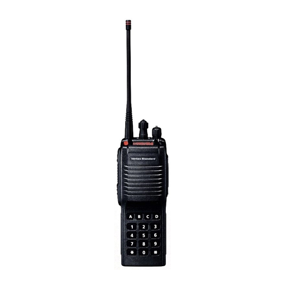
Operating Manual Reprint & C ONTROLS ONNECTORS CH ( Channel ) Selector LED Indicator Steady Green: Signaling off Blinking Green: Busy Channel (or SQL off) Steady Red: Transmission in Progress Antenna Jack Blinking Red: Battery voltage is low TOP SEL Key VOL/PWR Knob TOGGLE Switch LCD ( Liquid Crystal Display ) - Page 3 “Click.” the basic operation of the VX-900. Operation Quick Start Tilt the Belt Clip r Turn the top panel’s VOL/ PWR knob clockwise to turn on the radio on.
- Page 4 Operating Manual Reprint TOR button twice) to r Switch the top panel’s quiet the noise and re- TOGGLE switch to the sume normal (quiet) [A], [B] or [Center] posi- monitoring. tion to activate one of the pre-programmed func- tions which may have been enabled at the time of programming by the dealer.
- Page 5 PERATION Soft key and TOGGLE switch Functions TOGGLE switch ( Position ) The VX-900 includes the [ TOP SEL ] , [ SIDE SEL ] , Functions [ MONITOR ] , and [ LAMP ] keys, and the TOGGLE center...
- Page 6 Operating Manual Reprint DVANCED PERATION Description of Operating Functions High/Low Power Press the assigned Soft key or switch the Toggle Channel Scan switch to the assigned position to set the radio’s trans- The Scanning feature is used to monitor multiple sig- mitter to the “Low Power”...
- Page 7 PERATION possible to talk to the other station. Channel Group Selection The VX-900 is capable of separating its 512 memory Remember that disabling the encryption will mean that channels into any of 20 Groups. There is no limit as to your transmissions are no longer secure.
- Page 8 "OUT OF Emergency SERVICE" will scroll on the LCD. If you subse- The VX-900 includes an “Emergency” feature which quently move back into range, as soon as the other may be useful if you have someone monitoring on the station transmits, your beeper will sound, and "IN...
- Page 9 3-wire Earpiece, Mic, Palm PTT Switch VHF Antenna, 134 ~ 174 MHz (Untuned) Availability of accessories may vary; some accessories are supplied standard per local requirements, others may be unavailable in some regions. Check with your VERTEX STANDARD Dealer for changes to the this list.
-
Page 10: Set (Menu) Mode Functions
After selecting this Menu item, press the [TOP SEL] The VX-900 Soft Keys include the [TOP SEL], [SIDE or [SIDE SEL] key to select the Scan List in which SEL], [MON], and [LAMP] Keys, plus the [A], [B], you wish to scan ("LIST DLR: Dealer List"... - Page 11 Set (Menu) Mode Functions [SIDE SEL] key to select "P" (PTT Lock), "D" (Dial- No.11 ENCR (Encryption) Knob-Lock), "K" (Keypad Lock), or various combi- On channels where scrambling is used, an incorrect nations of these. Rotate the CH selector knob to save setting of (or failure in) the encryption system at one the new setting, then press the PTT switch to exit end of the communication path will make it impos-...
-
Page 12: Cloning
(“LOADING” will appear on the LCD). ceiver to be transferred to another VX-900. Here is 6. Press the PTT switch on the Source transceiver; the procedure for Cloning one radio’s data to an- “SENDING”... -
Page 13: Specifications
Specifications ENERAL Number of Channels: 512 channels Frequency Range: 134 - 160 MHz (A), 148 - 174 MHz (C) Channel Spacing: 12.5 / 20 / 25 kHz PLL Steps: 5 / 6.25 kHz Power Supply Voltage: 7.4 VDC ± 20 % Battery Life (5-5-90 duty): w/ FNB-V68LI (1800 mAh): 13 hrs. -
Page 14: Exploded View & Miscellaneous Parts
Exploded View & Miscellaneous Parts RA0297600 EXT CAP RA029850B FRONT CASE ASS'Y (16KEY) RA0215400 À SHEET RA0297300 Ç HOOK Ç RA0306900 (x2 pcs) COIL SPRING RA030720A KNOB RA029860B RA0297500 FRONT CASE ASS'Y (KEYLESS) RUBBER KNOB RA0317300 RA030770B LIGHT SHEET B M4090153 KNOB RA0297000... -
Page 15: Block Diagram
Block Diagram... - Page 16 Block Diagram Note:...
-
Page 17: Circuit Description
Circuit Description ters XF1001 and XF1002 (MDF0029, ±5.5 kHz BW) Overview to strip away all undesired mixer products. The VX-900 is a VHF FM hand-held transceiver de- signed to operate in the frequency range of 134 to IF Amplifier 174 MHz. - Page 18 Circuit Description The resulting DC squelch control voltage is passed If a CDCSS code is enabled for transmission, the code to pin 19 of the microprocessor Q1040. If no carrier is generated by Q1021 and delivered to D1049 is received, this signal causes pin 6 of Q1055 (HVC350) for CDCSS modulation.
- Page 19 Circuit Description Transmit Inhibit eighth multiple of the channel step size (5, 6.25 or When the Transmit PLL is unlocked, pin 18 of PLL 7.5 kHz). The input signal from pins 5 and 8 of the chip Q1045 goes to logic "low." The resulting DC PLL IC is divided down to 40 or 50 kHz and com- "unlock"...
-
Page 20: Alignment
Introduction ment is not covered under the warranty policy. While The VX-900 is carefully aligned at the factory for most steps do not require all of the equipment listed, the specified performance across the frequency the interactions of some adjustments may require range specified for each version. - Page 21 When connecting the CT-71 plug into the MIC/ The alignment tool consists of an executable file SP jack of the VX-900, you must remove the “SVC39.exe” and an accompanying configuration plastic cap and its mounting screws prior to file “SVC39.cfg”...
- Page 22 Alignment portant that you follow the basic alignment sequence • Press the [p] or [q] key, as needed, to set the precisely, so that the displayed data and the data power output to 5 Watts, as indicated on the ex- loaded into the transceiver are identical.
- Page 23 Alignment • Use the [t] or [u] key to select the "MID" fre- (1) Common RX : - [0] T quency channel in the alignment range. IGHT OISE QUELCH This parameter is used to align the "Tight Noise • Disable any subaudible tone signaling on this Squelch"...
- Page 24 Alignment • Press the [p] or [q] key, as needed, to set the Channels The following parameters may be adjusted individu- deviation to the desired value (typically 3.9~4.2 ally for each channel. For example, minor variations kHz, or 2.0~2.3 kHz for "narrow band" channels). in the power output across the operating band may •...
-
Page 25: Test Adapter Schematic
N.C. Yellow (Pin 7: Clone) Note! Because of the bridge audio amplifier circuit used in the VX-900, it is necessry to construct and use a simple audio load test adapter as shown in the schematic diagram above, when con- ducting receiver alignment steps. - Page 26 Note:...
-
Page 27: Main Unit
Main Unit Circuit Diagram 4.7V (0V) 2.7V 2.5V 1.0V -1dBµ (0V) (0V) (0V) -11dBµ +6dBµ 3.0V 0.6V (0V) (0V) -5dBµ (0.9V) -8dBµ WIDE: 3.2V 4.2V NARROW: 0V 3.8V (4.2V) 2.8V 5.0V (3.0V) 0.9V PO 5W: 3.9V 3.0V (2.6V) 7.4V (5.0V) 4.2V 0.8V 4.3V... - Page 28 Main Unit Note:...
- Page 29 Main Unit Parts Layout Side A UMZ2N (Z2) PDTC114TE TDA2822D NJM2902V CPH6102 (AB) UMG2N (G2) PDTC144EE (26) TK71635SCL (L35) XN1501 (5R) (Q1008, 1036) (Q1007) (Q1006, 1048, 1053, 1054) (Q1012,1049) (Q1013, 1017, 1068) (Q1035) (Q1011) (Q1015, 1016) (Q1034) LC87F72C8A UN911F (60) DA221 (K) S-80735SN-DZ (DZ) S-93C56AMFN...
- Page 30 Main Unit Side B XP1501 (5R) UMG2N (G2) TK71650SCL (L50) UN911F (60) PDTC114TE CPH6102 (AB) 2SD1767 (DC) PF0314-04 M62364FP (Q1003) (Q1004) (Q1005) (Q1009, 1018) (Q1014) (Q1023, 1028) (Q1002) (Q1010) (Q1019) AK2345 (Q1021) 2SC4617 (BR) TA31136FN SA7025DK RB715F (3D) DA221 (K) GN2011-Q (4W) PDTC144EE (26) (Q1030, 1043, 1044)
- Page 31 Main Unit (Lot. 6~) Circuit Diagram 4.7V (0V) 1.0V 2.7V 2.5V -1dBµ (0V) (0V) (0V) -11dBµ +6dBµ 3.0V 0.6V (0V) (0V) -5dBµ (0.9V) -8dBµ WIDE: 3.2V 4.2V NARROW: 0V 3.8V (4.2V) 2.8V 5.0V (3.0V) 0.9V PO 5W: 3.9V 3.0V (2.6V) 7.4V (5.0V) 4.2V...
- Page 32 Main Unit (Lot. 6~) Note:...
- Page 33 Main Unit (Lot. 6~) Parts Layout Side A UMZ2N (Z2) PDTC114TE TDA2822D NJM2902V CPH6102 (AB) UMG2N (G2) PDTC144EE (26) TK71635SCL (L35) XN1501 (5R) (Q1007) (Q1008, 1036) (Q1006, 1048, 1053, 1054) (Q1011) (Q1012,1049) (Q1013, 1017, 1068) (Q1035) (Q1015, 1016) (Q1034) LC87F72C8A UN911F (60) DA221 (K) S-80735SN-DZ (DZ)
- Page 34 Main Unit (Lot. 6~) Side B XP1501 (5R) UMG2N (G2) TK71650SCL (L50) UN911F (60) PDTC114TE CPH6102 (AB) 2SD1767 (DC) PF0314-04 M62364FP (Q1003) (Q1005) (Q1009, 1018) (Q1002) (Q1004) (Q1014) (Q1019) (Q1023, 1028) (Q1010) AK2345 (Q1021) 2SC4617 (BR) TA31136FN SA7025DK DA221 (K) PDTC144EE (26) RB715F (3D) GN2011-Q (4W)
- Page 35 Main Unit (Lot. 10~) Circuit Diagram 4.7V (0V) 1.0V 2.7V 2.5V -1dBµ (0V) (0V) (0V) -11dBµ +6dBµ 3.0V 0.6V (0V) (0V) -5dBµ (0.9V) -8dBµ WIDE: 3.2V 4.2V NARROW: 0V 3.8V (4.2V) 2.8V 5.0V (3.0V) 0.9V PO 5W: 3.9V 3.0V (2.6V) 7.4V (5.0V) 4.2V...
- Page 36 Main Unit (Lot. 10~) Note:...
- Page 37 Main Unit (Lot. 10~) Parts Layout Side A UMZ2N (Z2) PDTC114TE TDA2822D NJM2902V CPH6102 (AB) UMG2N (G2) PDTC144EE (26) TK71635SCL (L35) XN1501 (5R) (Q1007) (Q1008, 1036) (Q1006, 1048, 1053, 1054) (Q1011) (Q1012,1049) (Q1013, 1017, 1068) (Q1035) (Q1015, 1016) (Q1034) LC87F72C8A UN911F (60) DA221 (K) S-80735SN-DZ (DZ)
- Page 38 Main Unit (Lot. 10~) Side B XP1501 (5R) UMG2N (G2) TK71650SCL (L50) UN911F (60) PDTC114TE CPH6102 (AB) 2SD1767 (DC) PF0314-04 M62364FP (Q1003) (Q1005) (Q1009, 1018) (Q1002) (Q1004) (Q1014) (Q1019) (Q1023, 1028) (Q1010) AK2345 (Q1021) 2SC4617 (BR) TA31136FN SA7025DK DA221 (K) PDTC144EE (26) RB715F (3D) GN2011-Q (4W)
- Page 39 Main Unit Parts List REF. DESCRIPTION VALUE TOL. MFR’S DESIG VXSTD P/N VERS. LOT. SIDE LAY ADR *** MAIN-UNIT *** PCB with Components (W/ VR-UNIT) CP6966001 VERSION C PCB with Components (W/ VR-UNIT) CP6966003 VERSION A Printed Circuit Board FR006530D Printed Circuit Board FR006530E Printed Circuit Board...
- Page 40 Main Unit REF. DESCRIPTION VALUE TOL. MFR’S DESIG VXSTD P/N VERS. LOT. SIDE LAY ADR C 1041 CHIP CAP. 15pF GRM36CH150J50PT K22178216 VERSION A C 1041 CHIP CAP. 18pF GRM36CH180J50PT K22178218 VERSION C C 1042 CHIP CAP. GRM36CH060D50PT K22178208 C 1042 CHIP CAP. GRM36CH060D50PT K22178208 C 1043 CHIP CAP.
- Page 41 Main Unit REF. DESCRIPTION VALUE TOL. MFR’S DESIG VXSTD P/N VERS. LOT. SIDE LAY ADR C 1086 CHIP CAP. 0.1uF GRM36B104K10PT K22108802 C 1087 CHIP CAP. 0.0047uF GRM36B472K25PT K22148830 C 1088 CHIP CAP. 0.1uF GRM36B104K10PT K22108802 C 1089 CHIP CAP. 0.001uF GRM36B102K50PT K22178809...
- Page 42 Main Unit REF. DESCRIPTION VALUE TOL. MFR’S DESIG VXSTD P/N VERS. LOT. SIDE LAY ADR C 1144 CHIP CAP. 18pF GRM36CH180J50PT K22178218 C 1145 CHIP CAP. 0.01uF GRM36B103K16PT K22128804 C 1146 CHIP CAP. GRM36CK020C50PT K22178204 C 1147 CHIP CAP. GRM36CK010C50PT K22178202 C 1148 CHIP CAP.
- Page 43 Main Unit REF. DESCRIPTION VALUE TOL. MFR’S DESIG VXSTD P/N VERS. LOT. SIDE LAY ADR C 1201 CHIP CAP. 0.1uF GRM36B104K10PT K22108802 C 1202 CHIP CAP. 0.001uF GRM36B102K50PT K22178809 C 1203 CHIP CAP. 15pF GRM36CH150J50PT K22178216 C 1204 CHIP CAP. 15pF GRM36CH150J50PT K22178216...
- Page 44 Main Unit REF. DESCRIPTION VALUE TOL. MFR’S DESIG VXSTD P/N VERS. LOT. SIDE LAY ADR C 1260 CHIP CAP. 0.01uF GRM36B103K16PT K22128804 C 1261 CHIP CAP. 0.01uF GRM36B103K16PT K22128804 C 1262 CHIP CAP. 0.1uF GRM36B104K10PT K22108802 C 1263 CHIP CAP. 0.1uF GRM36B104K10PT K22108802...
- Page 45 Main Unit REF. DESCRIPTION VALUE TOL. MFR’S DESIG VXSTD P/N VERS. LOT. SIDE LAY ADR CF1002 CERAMIC FILTER PBFC450R9DR H3900528 D 1001 DIODE MA2S111-(TX) G2070614 D 1002 DIODE MA2S111-(TX) G2070614 D 1003 DIODE MA2S111-(TX) G2070614 D 1004 DIODE HSU277TRF G2070118 D 1006 DIODE PTZ TE25 15A G2070692...
- Page 46 Main Unit REF. DESCRIPTION VALUE TOL. MFR’S DESIG VXSTD P/N VERS. LOT. SIDE LAY ADR D 1061 LED LNJ808K8SRA G2070790 D 1062 DIODE DA221 TL G2070178 D 1063 DIODE MA2S111-(TX) G2070614 DS1001 LCD TA00171 G6090144 F 1001 CHIP FUSE 3.15A KAB-2402-322NA31 Q0000087 J 1001...
- Page 47 Main Unit REF. DESCRIPTION VALUE TOL. MFR’S DESIG VXSTD P/N VERS. LOT. SIDE LAY ADR Q 1003 TRANSISTOR XP1501-(TX) G3070143 Q 1004 TRANSISTOR UMG2N TR G3070088 Q 1005 IC TK71650SCL G1093136 Q 1006 TRANSISTOR PDTC114TE G3070238 Q 1007 TRANSISTOR UMZ2N TR G3070117 Q 1008 TRANSISTOR CPH6102-TL...
- Page 48 Main Unit REF. DESCRIPTION VALUE TOL. MFR’S DESIG VXSTD P/N VERS. LOT. SIDE LAY ADR R 1002 CHIP RES. 1/16W RMC1/16S 102JTH J24189025 R 1003 CHIP RES. 1/16W RMC1/16S 102JTH J24189025 R 1004 CHIP RES. 1/16W RMC1/16S 102JTH J24189025 R 1005 CHIP RES. 1/16W RMC1/16S 103JTH J24189037...
- Page 49 Main Unit REF. DESCRIPTION VALUE TOL. MFR’S DESIG VXSTD P/N VERS. LOT. SIDE LAY ADR R 1064 CHIP RES. 150k 1/16W RMC1/16S 154JTH J24189051 R 1065 CHIP RES. 1/16W RMC1/16S 123JTH J24189038 R 1066 CHIP RES. 100k 1/16W RMC1/16S 104JTH J24189049 R 1067 CHIP RES.
- Page 50 Main Unit REF. DESCRIPTION VALUE TOL. MFR’S DESIG VXSTD P/N VERS. LOT. SIDE LAY ADR R 1125 CHIP RES. 1/16W RMC1/16S 681JTH J24189023 R 1126 CHIP RES. 2.2k 1/16W RMC1/16S 222JTH J24189029 R 1127 CHIP RES. 1/16W RMC1/16S 101JTH J24189013 R 1128 CHIP RES.
- Page 51 Main Unit REF. DESCRIPTION VALUE TOL. MFR’S DESIG VXSTD P/N VERS. LOT. SIDE LAY ADR R 1184 CHIP RES. 4.7k 1/16W RMC1/16S 472JTH J24189033 R 1185 CHIP RES. 1/16W RMC1/16S 103JTH J24189037 R 1186 CHIP RES. 330k 1/16W RMC1/16S 334JTH J24189055 R 1187 CHIP RES.
- Page 52 Main Unit REF. DESCRIPTION VALUE TOL. MFR’S DESIG VXSTD P/N VERS. LOT. SIDE LAY ADR R 1245 CHIP RES. 1/16W RMC1/16S 102JTH J24189025 R 1246 CHIP RES. 1/16W RMC1/16S 102JTH J24189025 R 1247 CHIP RES. 1/16W RMC1/16S 102JTH J24189025 R 1248 CHIP RES. 1/16W RMC1/16S 102JTH J24189025...
- Page 53 Main Unit REF. DESCRIPTION VALUE TOL. MFR’S DESIG VXSTD P/N VERS. LOT. SIDE LAY ADR R 1305 CHIP RES. 1/16W RMC1/16S 393JTH J24189044 R 1305 CHIP RES. 1/16W RMC1/16S 473JTH J24189045 VERSION A R 1305 CHIP RES. 1/16W RMC1/16S 393JTH J24189044 VERSION C R 1306 CHIP RES.
- Page 54 Main Unit REF. DESCRIPTION VALUE TOL. MFR’S DESIG VXSTD P/N VERS. LOT. SIDE LAY ADR XF1002 XTAL FILTER HDF0029 22.05MHZ H1102336 XF1002 XTAL FILTER HDF0029 22.05MHZ H1102336 HOLDER PLATE (TGL) RA0207700 MIC HOLDER RUBBER RA0140200 SHIELD CASE VCO RA0208100 MIC HOLDER RUBBER RA0207800 HOLDER PLATE (PM)
-
Page 55: Vr Unit
VR Unit Circuit Diagram Parts Layout BRPY1211F (D5002) Side A Side B Parts List REF. DESCRIPTION VALUE TOL. MFR’S DESIG VXSTD P/N VERS. LOT. SIDE LAY ADR *** VR-UNIT *** PCB with Components CB1439001 Printed Circuit Board FR006580E D 5001 LED FA1111C-TR G2070836 D 5001 LED... -
Page 56: Sw Unit
SW Unit Circuit Diagram Parts Layout Side A Side B Parts List REF. DESCRIPTION VALUE TOL. MFR’S DESIG VXSTD P/N VERS. LOT. SIDE LAY ADR *** SW-UNIT *** PCB with Components CB1437001 Printed Circuit Board FR006570B S 3001 TACT SWITCH SOP-114HST R66-5374 N5090107 S 3002 TACT SWITCH... -
Page 57: Dummy Unit
Dummy Unit Circuit Diagram Parts Layout Component Side Parts List REF. DESCRIPTION VALUE TOL. MFR’S DESIG VXSTD P/N VERS. LOT. SIDE LAY ADR *** DUMMY-UNIT *** PCB with Components CB1438001 Printed Circuit Board FR002510C C 4001 CHIP CAP. 0.0018uF GRM39B182M50PT K22174812 C 4002 CHIP CAP. -
Page 58: F2D-8 2-Tone Decode Unit
F2D-8 2-Tone Decode Unit Circuit Diagram Parts Layout Side A Side B TC7S04FU (E5) TA75S01F (SA) DTC124TU (05) HD64F3334YTF16 (Q1003) (Q1004) (Q1005) (Q1001) - Page 59 F2D-8 2-Tone Decode Unit Parts List REF. DESCRIPTION VALUE TOL. MFR’S DESIG VXSTD P/N VERS. LOT. SIDE LAY ADR *** F2D-8 *** Printed Circuit Board FR002530C C 1001 CHIP TA.CAP. 4.7uF 6.3V TEMSVA0J475M-8R K78080017 C 1002 CHIP CAP. 0.001uF GRM39B102K50PT K22174821 C 1003 CHIP CAP.
-
Page 60: Vtp-50 Vx-Trunk Unit
VTP-50 VX-Trunk Unit Circuit Diagram Parts Layout Side B Side A NJM2904V TA75S01F (SA) BR93LC56FV MC68HSC705C8A502 (Q1001) (Q1002) (Q1003) (Q1004) - Page 61 VTP-50 VX-Trunk Unit Parts List REF. DESCRIPTION VALUE TOL. MFR’S DESIG VXSTD P/N VERS. LOT. SIDE LAY ADR *** VTP-50 *** Printed Circuit Board FR002540C C 1002 CHIP CAP. 0.001uF GRM39B102K50PT K22174821 C 1003 CHIP CAP. 0.01uF GRM39B103M25PT K22144802 C 1003 CHIP CAP. 0.01uF GRM39B103K25PT K22144803...
-
Page 62: Fvp-25 Encryption / Dtmf Pager Unit
FVP-25 Encryption / DTMF Pager Unit Circuit Diagram Parts Layout Side A Side B M64026FP LC73881 DTC144EU (26) (Q1001) (Q1002) (Q1003) - Page 63 FVP-25 Encryption / DTMF Pager Unit Parts List REF. DESCRIPTION VALUE TOL. MFR’S DESIG VXSTD P/N VERS. LOT. SIDE LAY ADR *** FVP-25 *** Printed Circuit Board FR005010F C 1001 CHIP CAP. 0.1uF GRM39B104K16PT K22124805 C 1002 CHIP CAP. 0.01uF GRM39B103M25PT K22144802 C 1003 CHIP CAP.
-
Page 64: F5D-14 5-Tone Unit
F5D-14 5-Tone Unit Circuit Diagram Parts Layout Side A Side B TK71650SC (L50) DTC114TE (04) PIC17LC44-08/PQ 2SC4617 (BR) MD09 BR93LC66FV (Q1001) (Q1002) (Q1003) (Q1004) (Q1005) (Q1006) - Page 65 F5D-14 5-Tone Unit Parts List REF. DESCRIPTION VALUE TOL. MFR’S DESIG VXSTD P/N VERS. LOT. SIDE LAY ADR *** F5D-14 *** Printed Circuit Board FR006510B Printed Circuit Board FR006510D C 1001 CHIP CAP. 0.1uF GRM36B104K10PT K22108802 C 1002 CHIP CAP. 0.0018uF GRM36B182K50PT K22178812...
- Page 66 No portion of this manual may be © Copyright 2002 reproduced without the permission of VERTEX STANDARD CO., LTD. VERTEX STANDARD CO., LTD. All rights reserved Printed in Japan.
Need help?
Do you have a question about the VX-900 and is the answer not in the manual?
Questions and answers