Advertisement
One Technology Way • P.O. Box 9106 • Norwood, MA 02062-9106, U.S.A. • Tel: 781.329.4700 • Fax: 781.461.3113 •
Evaluation Board for the ADA4432-1, Video Filter Amplifier
FEATURES
Fully assembled and tested
Enables quick customer evaluation
Edge-mounted SMA connector provisions
Easy connection to test equipment and other circuits
GENERAL DESCRIPTION
The
ADA4432-1BCP-EBZ
evaluation board makes it easy for
designers to quickly observe the performance of the
video filter LFCSP package in a real-world application. The
ADA4432-1BCP-EBZ
uses the same printed circuit board (PCB)
as the
ADA4433-1BCP-EBZ,
its configuration is optimized for the ADA4432-1.
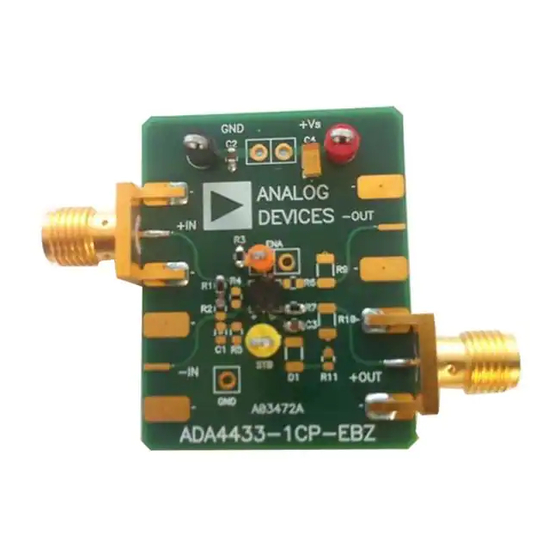
Input signals are applied through the SMA jack (+IN), and
output signals are taken from the SMA jack (+OUT). Power is
applied through the red +VS test point. Ground the black GND
test point. The
ADA4432-1
operates on a single-supply voltage
ranging from 2.7 V to 3.6 V and draws approximately 7 mA.
The evaluation board is configured with an input termination
resistor (R1) of 75 Ω. Choose this resistor to provide the correct
termination or load for the input signal source. For example,
some video encoders use current mode video digital-to-analog
NOTES
1. THE EVALUATION BOARD SILKSCREEN PART NUMBER LABELING ON
YOUR BOARD MAY BE DIFFERENT FROM WHAT IS SHOWN HERE.
Figure 1.
ADA4432-1BCP-EBZ
PLEASE SEE THE LAST PAGE FOR AN IMPORTANT
WARNING AND LEGAL TERMS AND CONDITIONS.
Offered in 8-Lead LFCSP
ADA4432-1
and it is marked as such; however,
EVALUATION BOARD, PRIMARY SIDE AND SECONDARY SIDE
Evaluation Board, Primary Side
Evaluation Board User Guide
converter (DAC) outputs that require a 300 Ω load resistance.
In this case, replace R1 with a 300 Ω resistor.
The
ADA4432-1BCP-EBZ
a back terminated 150 Ω load. A series back-termination resistor
of 75 Ω is installed on the output at R7. If the input impedance
of the load is different from 75 Ω, then R7 can be changed to
match the actual load impedance.
The
ADA4432-1
the orange ENA test point at the top left of the evaluation board.
On the evaluation board, this pin is pulled up to +VS through
the 4.99 kΩ resistor (R3).
In normal operation, the short-to-battery output flag (STB) is held
at a logic low. During a short-to-battery fault condition (where
a voltage ranging from 5 V to 18 V is applied to either or both
outputs), the STB output voltage is driven to a logic high state.
The STB yellow test point (lower left side of the evaluation board)
can be used to monitor the short-to-battery output flag function.
Figure 1 and Figure 2 show the evaluation board primary side
and secondary side, respectively. Figure 3 shows the evaluation
board schematic. The PCB layout pattern for the primary side
and secondary side are shown in Figure 4 and Figure 5.
Figure 2.
ADA4432-1BCP-EBZ
Rev. 0 | Page 1 of 4
evaluation board is configured to drive
can be powered down (disabled) by grounding
Evaluation Board, Secondary Side
UG-462
www.analog.com
Advertisement
Table of Contents

Subscribe to Our Youtube Channel
Related Manuals for Analog Devices ADA4432-1BCP-EBZ


Summary of Contents for Analog Devices ADA4432-1BCP-EBZ
- Page 1 (DAC) outputs that require a 300 Ω load resistance. In this case, replace R1 with a 300 Ω resistor. Fully assembled and tested ADA4432-1BCP-EBZ evaluation board is configured to drive Enables quick customer evaluation a back terminated 150 Ω load. A series back-termination resistor Edge-mounted SMA connector provisions of 75 Ω...
- Page 2 UG-462 Evaluation Board User Guide TABLE OF CONTENTS Features ....................1 Evaluation Board Schematic and Artwork ........3 General Description ................. 1 Ordering Information ...............4 Evaluation Board, Primary Side and Secondary Side ....1 Bill of Materials ................4 Revision History ................2 REVISION HISTORY 8/12—Revision 0: Initial Version Rev.
- Page 3 ADA4432-1 NC STB +OUT 75Ω +OUT 0.1µF 0.1µF 10µF 333Ω Figure 3. ADA4432-1BCP-EBZ Evaluation Board Circuit Schematic Figure 4. ADA4432-1BCP-EBZ Board Layout Pattern, Primary Side Figure 5. ADA4432-1BCP-EBZ Board Layout Pattern, Secondary Side Rev. 0 | Page 3 of 4...
- Page 4 By using the evaluation board discussed herein (together with any tools, components documentation or support materials, the “Evaluation Board”), you are agreeing to be bound by the terms and conditions set forth below (“Agreement”) unless you have purchased the Evaluation Board, in which case the Analog Devices Standard Terms and Conditions of Sale shall govern. Do not use the Evaluation Board until you have read and agreed to the Agreement.
Need help?
Do you have a question about the ADA4432-1BCP-EBZ and is the answer not in the manual?
Questions and answers