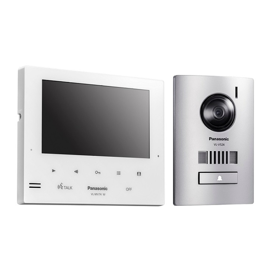
Panasonic VL-SV75 Series Service Manual

Panasonic VL-SV75 Series Service Manual

Video intercom system
Table of Contents

Advertisement

Video Intercom System
VL-SV75AZ
Model No.
VL-MV75AZ
VL-MV75AZA
VL-MV75BXA
VL-V524LCE
VL-PS241
© Panasonic Corporation 2019
Unauthorized copying and distribution is a violation of law.
Order No.KMA1911121CE

Advertisement

Table of Contents
loading

Summary of Contents for Panasonic VL-SV75 Series

  • Page 1 Order No.KMA1911121CE Video Intercom System VL-SV75AZ Model No. VL-MV75AZ VL-MV75AZA VL-MV75BXA VL-V524LCE VL-PS241 © Panasonic Corporation 2019 Unauthorized copying and distribution is a violation of law.
  • Page 3: Table Of Contents

    Table of Contents Page Page 1. Safety Precautions............5 8.1.1. Main Monitor Station............20 1.1. For Service Technicians............5 9. Troubleshooting Guide..........21 1.2. Insulation Resistance Test (by Insulation resistance 9.1. Operation Check of the Door Station........ 21 tester).....................5 9.2. Operation Check of the Main Monitor Station....25 1.3.
  • Page 4 10.2.4. How to Remove the Mic Board and Speaker [No.4]..49 13.2.1. Main Board..............72 10.2.5. Installation of the lead wires..........51 13.2.2. MIC Board..............73 10.2.6. Item to be checked after completion of assembly 13.3. Power Supply Unit.............74 (camera lens angle adjustment)..........51 13.3.1.
  • Page 5: Safety Precautions

    1 Safety Precautions 1. Before servicing, unplug the power cord to prevent an electrical shock. 2. When replacing parts, use only manufacturer’s recommended components for safety. 3. Check the condition of power cord. Replace if wear or damage is evident. 4. After servicing, be sure to restore the lead dress, insulation barriers, insulation papers, shields, etc. 5.
  • Page 6: Warning

    2 Warning 2.1 Battery Caution Risk of explosion if battery is replace by an incorrect type. Dispose of used batteries according to the instructions. 2.2 About Lead Free Solder (PbF: Pb free) Note: In the information below, Pb, the symbol for lead in the periodic table of elements, will refer to standard solder or solder that contains lead.
  • Page 7: Discarding Of P.c. Board

    2.3 Discarding of P.C. Board When discarding P. C. Board, delete all personal information such as telephone directory, caller list and recorded images or scrap P. C. Board. 2.4 Note For Repairing 1. Before carrying out repair, inform the user that there is a possibility of the user data inside the equipment becoming lost. 2.
  • Page 8: Specifications

    3 Specifications Design and specifications are subject to change without notice. 3.1 Main monitor station (VL-MV75) Power source: Power supply unit (VL-PS241) 24 V DC, 0.5 A Power consumption: Standby: 1.9 W During operation: 12.7 W Dimensions (mm): VL-MV75-S VL-MV75-W : approx. 158 x 201 x 25 (excluding protruding sections) (height x width x depth) VL-MV75-M : approx.
  • Page 9: Technical Descriptions

    4 Technical Descriptions 4.1 Block Diagram The block diagram of Video intercom system is shown in Fig 4.1. Image signal root: The image data is converted into NTSC signal by Camera unit, and the NTSC signal is modulated into FM signal. FM signal is sent to the Monitor station through the interphone cable with ASK signal which modulated from command signal and voice signal.
  • Page 10 Call Signal from Door station: When the call button is pressed in Stand-by mode, the short between lines causes the DC voltage of the interphone cable to go down. The monitor station detects this voltage reduction and then rings. Then LCD of the Monitor station is turned ON. Fig.
  • Page 11: Ic Operation

    4.2 IC Operation 4.2.1 Monitor Station Section 4.2.1.1 Main Monitor station Diagram - 11 -...
  • Page 12 4.2.1.2 Main Board 4.2.1.2.1 External Interface Part Regulator for 5V (IC671) Regulator for Power 5V (IC910) Input voltage: +12V Input voltage: +12V Output voltage: +5V Output voltage: +5V Package: 5pin SOT-25A. Package: 8pin SOP-8 Outline of Operation: It generate from +12V to +5V (FM Outline of Operation: It generate from +12V to +5V.
  • Page 13 4.2.1.2.2 Audio Part EEPROM(IC401) Sub CPU (IC405) Operating Power Supply : +3.3V Operating Power Supply : +3.3V Package: SOP-J8 Operating Power Supply : +4V (SP AMP) Memory capacity: 64kbit Operating Power Supply : +3.2V (RF) Outline of Operation: Storing the parameter of IC405. Operating Power Supply : +1.8V (Core) Package: 206pin 1MSRAM (IC404)
  • Page 14 4.2.1.3 Power Board 4.2.1.3.1 Power Supply Part Regulator for Power 12V (IC1) Input voltage: +24V Output voltage: +12V Package: 6pin SOT-23-6W Outline of Operation: It generate from +24V to +12V. 4.2.1.4 KEY Board 4.2.1.4.1 Key Part Regulator for Power 3.3V (IC1001) Input voltage: +5V Output voltage: +3.3V Package: 5pin SOT-89-5 Outline of Operation: It generate from +5V to +3.3V.
  • Page 15: Door Station Section

    4.2.2 Door Station Section 4.2.2.1 Door station Diagram - 15 -...
  • Page 16 4.2.2.2 Main Board Call Button (SW301) Outline of Operation : When a visitor presses the Call Button, a chime tone will ring at the monitor station. FM Signal Modulator (IC200) Operating Power Supply : +5V (+5V : 2, 9pin) Package : 24pin SOP Outline of Operation : The frequency modulation of the video signal taken in from Camera Unit is carried out.
  • Page 17: Location Of Controls And Components

    5 Location of Controls and Components Refer to the Operating Instructions. Note: You can download and refer to the Operating Instructions (Instruction book) on TSN Server. - 17 -...
  • Page 18: Installation Instructions

    6 Installation Instructions Refer to the Operating Instructions. Note: You can download and refer to the Operating Instructions (Instruction book) on TSN Server. - 18 -...
  • Page 19: Operating Instructions

    7 Operating Instructions Refer to the Operating Instructions. Note: You can download and refer to the Operating Instructions (Instruction book) on TSN Server. - 19 -...
  • Page 20: Service Mode

    8 Service Mode 8.1 Things to do after replacing IC If repairing FLASH Memory, EEPROM, it is necessary to initialize and adjustment. The set doesn't operate if it is not executed. 8.1.1 Main Monitor Station Preparation 1. Serial JIG cable: PQZZ1CD300E 2. PC in which "Tera Term (Ver. 4.78 later)" (communication software) is installed 3.
  • Page 21: Troubleshooting Guide

    9 Troubleshooting Guide 9.1 Operation Check of the Door Station START Advance preparation: Connect the Door Station to nondefective Main Monitor Station. Call from the Door Station. Does the ringtone Is the image displayed? sound from the Main Monitor Station? Is it possible to respond from Is it possible to respond from the main monitor station? the main monitor station?
  • Page 22 START Does the LED on the button of the Is the wiring correct Door Station light in standby mode? between the Main Monitor Station and (Is the voltage between terminals of the Door Station? the Door Station about 4~5V?) Rewire the Main Monitor Station and the Door Station correctly.
  • Page 23 No image can be seen by the call from the Door Station. (The ringer tone and the talking are OK.) Is the FM signal at pin3 of IC200 on the Main Board of the Door Station OK? (Refer to Fig.1) Check Signal Flow of the Image Signal (Door Station) Main Board Measuring conditions (FM signal):...
  • Page 24 If the front side of When lighting operation is door station is made dark, carried out with the Monitor Station, does lighting turn on does lighting turn on? automatically? Are there any missing /faulty parts around LED200 and LED201? Replace the Main board. Replace the fault parts.
  • Page 25: Operation Check Of The Main Monitor Station

    9.2 Operation Check of the Main Monitor Station START Advance preparation: Connect the Main Monitor Station to non-defective Door Station and Extension Monitor. *Make sure the power is ON by pressing the talk key, etc. Is the unit powered ON? Go to "Defect of the Main Monitor Station power supply "(*1). Register a normal Extension Monitor with the Main Monitor Station.
  • Page 26: Defect Of The Communication Between The Main Monitor Station And The Extension Monitor

    9.2.1 Defect of the Communication Between the Main Monitor Station and the Extension Monitor START Advance preparation: Connect a non-defective Door Station and the Extension Monitor to the Main Monitor Station. Communicate between the Extension Monitor and the Door Station. Can the video/voice communication be made? Are all parts on Talk Signal Path (Transmitting)
  • Page 27: Defect Of The Extension Monitor Video Recording

    9.2.2 Defect of the Extension Monitor Video Recording START Advance preparation: Connect a non-defective Door Station and the Extension Monitor to the Main Monitor Station. Communicate between the Door Station and the Extension Monitor. Is it possible to record / play an image of the door station? Are all parts on Recording Image Operation...
  • Page 28: Defect Of The Main Monitor Station Power Supply

    9.2.3 Defect of the Main Monitor Station Power Supply 9.2.3.1 Defect of the Power supply unit START Are the AC cable connected to Is the unit powerd ON? Rewire the AC cable correctly. power unit properly? Replace with a non-defective power supply unit. Is the unit powerd ON? Go to "Defect of the power supply unit".(See below) Is the wiring of...
  • Page 29 9.2.3.2 Defect of the Power board unit Defect of the Power board unit Is the voltage of C1 Replace fuse(F1)on Power Board Is the unit powered (Power board) about of the Main Monitor Station. ON ? 24V? Check around LF1 Is the voltage of C3 Replace the Is the unit powered L1,L2,D1,D2,D3,D4...
  • Page 30 9.2.3.3 Defect of the Main board unit Detect of the Main unit power supply Check around Q31, Is the voltage of Replace the D31,R32,R31 and Is the unit powered C903 about 22V? fault parts. C34 of Main Board. ON ? Is the voltage of C904 Replace fuse(F900) on Main Board of Is the unit powered (Main Board) about...
  • Page 31 (from previous page) Check around IC930, L930,R931,R932,R933, Is the voltage of Replace the Is the unit powered C930,C932,C933,C934, CL930(Main Board) about fault parts. ON ? C935 and C937 4V?(12V→4V) of Main Board. Check around IC920, Is the voltage of L920,R921,R922,R923, Replace the Is the unit powered CL920(Main Board) about...
  • Page 32 (from previous page) Is the voltage of Check around Q230, Replace the Is the unit powered CL230(Main Board) about R230,R231, fault parts. ON ? 3.3V for LCD? of Main Board. Check around L230, Is the voltage of IC230,R256,C238,D232, Replace the Is the unit powered CL231(Main Board) about R237,R238,C241,C243...
  • Page 33: Defect Of The Main Monitor Station Video Recording

    9.2.4 Defect of the Main Monitor Station Video Recording START Advance preparation: Connect a non-defective Door Station to the Main Monitor Station. Communicate between the Door Station and the Main Monitor Station. Is it possible to record / play an image of the door station? Are all parts on Image Signal Path of...
  • Page 34: Defect Of The Communication Between The Main Monitor Station And The Door Station

    9.2.5 Defect of the Communication Between the Main Monitor Station and the Door Station START Advance preparation: Connect a non-defective Door Station to the Main Monitor Station. Communicate between the Main Monitor Station and the Door Station. Can the video/voice communication be made? Are all parts on Talk Signal Path (Transmitting) Replace the fault parts.
  • Page 35: Defect Of The Communication Between The Extension Monitor Station And The Door Station

    9.2.6 Defect of the Communication Between the Extension Monitor Station and the Door Station START Advance preparation: Connect a non-defective Door Station and Extension Monitor Station to the Main Monitor Station. Communicate between the Extension Monitor Station and the Door Station. Can the video/voice communication be made? Are all parts on...
  • Page 36: Defect Of The Key Board Unit

    9.2.7 Defect of the Key board unit START Confirm that the CL 910 of the main board becomes 5 V. Is the voltage of Is the cable connected to Connect the cables correctly. CL1001 about 5V? CN 701 and CN 1001? Is the voltage of Check around IC1001, Replace the...
  • Page 37: Signal Route

    9.3 Signal Route This chapter provides the testing procedures required for the P.C.B. parts. A signal route to be tested is determined depending upon purposes. The signal mainly flowing on this route is analog. You can trace the signal with an oscilloscope. The signal flow on each route is shown in the Check Sheet here.
  • Page 38 - 38 -...
  • Page 39 - 39 -...
  • Page 40 - 40 -...
  • Page 41 - 41 -...
  • Page 42 - 42 -...
  • Page 43: Disassembly And Assembly Instructions

    10 Disassembly and Assembly Instructions 10.1 Main Monitor Station 10.1.1 How to Remove the DC cable [No.1] Remove 2 screws (a). Remove the DC cable cover. Keep pressing the terminal by Screwdriver's head and pull out the wires of the DC cable as shown in Fig.1 10.1.2 How to Remove the Cabinet Cover [No.2] ■...
  • Page 44: How To Remove The Main Board, Speaker And Lcd [No.3]

    10.1.3 How to Remove the Main Board, Speaker and LCD [No.3] ■ Procedure No.1→No.2→No.3 Remove connector (Fig.2). Remove the solder of wires (Fig.3, Fig.4). Remove 2 screws (c). Remove the Main board with LCD holder from Cabinet body. Unhook the 4 tabs of the LCD holder. Remove the Flat cable from Main board as shown in Fig.5.
  • Page 45: How To Remove The Power Board, Key Board [No.4]

    10.1.4 How to Remove the Power board, Key board [No.4] ■ Procedure No.1→No.2→No.3→No.4 Remove 3 screws (d). Remove Power board from Cabinet body. Remove PCB holder from Cabinet body. Remove Key board from Cabinet body. - 45 -...
  • Page 46: Door Station

    10.2 Door Station 10.2.1 How to Remove the Front Panel [No.1] Unlock the hook by inserting the screw driver (Fig.A). Remove Front panel from Cabinet body. - 46 -...
  • Page 47: How To Remove The Door Station [No.2]

    10.2.2 How to Remove the Door Station [No.2] ■ Procedure No.1→No.2 Remove 4 screws (a). Case of Mounting base used Case of Flush mount box used - 47 -...
  • Page 48: How To Remove The Main Board And Camera Unit [No.3]

    10.2.3 How to Remove the Main Board and Camera Unit [No.3] ■ Procedure No.1→No.2→No.3 Remove 4 screws (b). Please remove the cabinet cover from cabinet body with care to the hooks. Remove the solder on the 3 pairs of lead wires (Fig.B, Fig.C, Fig.D). Disconnect the connector-A from the Camera Unit.
  • Page 49: How To Remove The Mic Board And Speaker [No.4]

    10.2.4 How to Remove the Mic Board and Speaker [No.4] ■ Procedure No.1→No.2→No.3→No.4 Remove the Mic board. Remove the Speaker. - 49 -...
  • Page 50 10.2.4.1 Note for Microphone Assembly (for anti-feedback) - 50 -...
  • Page 51: Installation Of The Lead Wires

    10.2.5 Installation of the lead wires When assembling the door station, route the lead wires as shown in the figure below, and be careful that they do not get caught. 10.2.6 Item to be checked after completion of assembly (camera lens angle adjustment) After completing assembly work, move the angle adjustment lever on the rear surface in the left and right directions, and confirm that it moves all the way.
  • Page 52: Power Supply Unit

    10.3 Power Supply Unit 1. Remove 4 screws (a). 2. Remove the Power Board by unhooking 2 tabs. - 52 -...
  • Page 53: Measurements And Adjustments

    11 Measurements and Adjustments 11.1 Main Monitor Station 11.1.1 Main Board 11.1.1.1 Connections When replacing the main board (Monitor Station), please refer to the following items for adjusting. - 53 -...
  • Page 54 11.1.1.2 When replacing BBIC and X'tal ■ Preparation: 1. PC setting refer to [8.1.1 Main Monitor Station]. 2. Supply AC 230V. Note: Test points: Refer to [14.1.2 Main Board (Bottom View)]. Items Check Point Procedure 1.8 V Supply Adjustment CL437(BB1.8V) Confirm that the voltage between test point CL437 and CL109 (GND) is 1.8 V ± 0.02 V.
  • Page 55: Factory Mode

    11.1.2 Factory Mode ■ Entering Factory Mode: Turn AC Power “ON”, while pressing [F5] button, about 5 seconds or more. Press [TALK] , [OFF],[F4] key sequentially. (FACTORY MODE screen is displayed.) ■ In order to exit Factory Mode: 1. Press the [F1] button. - 55 -...
  • Page 56 11.1.2.1 Factory Setup Initialize the logs and the all parameters except for the factory adjusted value, and delete the recorded images. 1. Select “FACTORY SETUP” by [F2] or [F3]. 2. Press [F4 (DECIDE)]. 3. Press [F4 (RUN)]. 4. Press [F1 (RESET)]. - 56 -...
  • Page 57 11.1.2.2 White Balance Adjustment The adjustment is done only when the color of the LCD display has changed after you have replaced the LCD. (Basically, adjustment is unnecessary.) 1. Select “TECHNICAL MODE 1” by [F2] or [F3]. Press [F4(DECIDE)]. 2. Select “WHITE BALANCE” by [F2] or [F3]. Press [F4(DECIDE)].
  • Page 58: Door Station

    4. Adjust the white balance by R Gain and B Gain. (1) Select the color to be adjust as below [F1] (>>): (Select Digit) • [F2] (▼), F3 (▲): (Change Value) • (2) Press [F4 (DECIDE)] (3) Adjust the white balance as below •...
  • Page 59: Miscellaneous

    12 Miscellaneous 12.1 How to Replace the Flat Package IC Even if you do not have the special tools (for example, a spot heater) to remove the Flat IC, with some solder (large amount), a soldering iron and a cutter knife, you can easily remove the ICs that have more than 100 pins. 12.1.1 Preparation •...
  • Page 60: Flat Package Ic Installation Procedure

    12.1.3 Flat Package IC Installation Procedure 1. Temporarily fix the FLAT PACKAGE IC, soldering the two marked pins. *Check the accuracy of the IC setting with the corresponding soldering foil. 2. Apply flux to all pins of the FLAT PACKAGE IC. 3.
  • Page 61: Schematic Diagram

    13 Schematic Diagram Note: 1. DC voltage measurements are taken with an oscilloscope or a tester with a ground. 2. The schematic diagrams and circuit board may be modified at any time with the development of new technology. - 61 -...
  • Page 62: Main Monitor Station

    13.1 Main Monitor Station 13.1.1 Main Board (1) / External I/F D627 R627 6.2V C627 0.1u 16 R621 330 R611 330 C612 C613 0.01u 0.01u R613 R615 C611 C621 R616 R614 1u 6.3 2.2k 2.2k D640 C630 R630 R623 R625 D611 D621 R624 R626 2.2k...
  • Page 63: Main Board (2) / Bbic

    13.1.2 Main Board (2) / BBIC DPJP3 CL573 CL572 CL574 D560 CL571 R584 D561 CF571 R588 C562 C563 100k 100k R565 R564 CF572 C565 C564 R400 3300p 3300p 4.7k R572 R573 R571 R574 R589 R583 100k C585 C575 6.3V 22uF 100k R590 C401 C589...
  • Page 64: Main Board (3) / Dpjp3_Key

    13.1.3 Main Board (3) / DPJP3_KEY C100 2200p D100 4.71V C102 4.7k 0.1u 16 R102 IC101 1 GND R107 C101 2 VDD 220p C111 C106 1000p 0.01u 25 C103 R110 C105 C107 C104 C340 NC C112 C113 1uF 16V 0.1u 1000p 0.01u C114 1uF C115 1uF...
  • Page 65: Main Board (4) / Lcd

    13.1.4 Main Board (4) / LCD C230 1uF 6.3V R230 R231 C231 Q230 10uF Gth=1.8V C232 0.1uF C233 D230 C234 0.1uF R235 2.2k C237 0.1uF C238 COMP 3300pF FCLK IC230 R238 21.5k C241 10uF D234 R241 8.2k C247 10uF C248 10uF R246 C201 47pF...
  • Page 66: Main Board (5) / External I/F_Electric Lock

    13.1.5 Main Board (5) / External I/F_Electric lock CL621 CL622 CL601 CL623 CL602 CL624 CL613 CL603 CL614 CL604 CL605 CL615 CL606 CL616 CL607 CL617 CL608 CL618 CL609 CL610 CL611 CL612 R880 R881 150 C881 150 C880 0.1u 0.1u D281 R281 RL880 RL881 D881 D880...
  • Page 67: Main Board (6) / Dcdc

    13.1.6 Main Board (6) / DCDC 220uF 220uF 150uF 470 1W 47u 35 C901 C900 10uF C903 0.1u C904 0.1u 50 C905 10uF C907 C902 0.01u 25 C906 10uF C921 C911 C930 C920 C910 10uF 10uF 10uF R931 R911 R921 R932 60.4k R922 R912...
  • Page 68: Main Board (7) / Am Communication_Base Unit

    13.1.7 Main Board (7) / AM communication_base unit L721 L728 C721 C724 L722 L729 C722 C725 L723 L730 C723 C729 C720 1500p D700 C730 C710 0.1u 16 C748 1000p R724 R728 100k R797 R729 2.2k 8.2k R798 VL-MV75: Main Board No.7: AM communication_base unit - 68 -...
  • Page 69: Main Board (8) / Am Communication_Add Base Unit

    13.1.8 Main Board (8) / AM communication_add base unit C761 1500p D759 C759 NC C763 C765 100p C766 100p R768 R762 NC R763 IC760 R770 AOUT 8.2k A-IN BOUT A+IN B-IN C777 C776 100p B+IN C772 NC C778 1000p C773 10uF C774 C487 1000p...
  • Page 70: Main Board (9) / Key

    13.1.9 Main Board (9) / KEY RX-VOL MENU TALK MONITOR PAD1 PAD2 PAD3 PAD4 PAD5 PAD6 PAD7 T3V3 CL1007 CL1001 T3V3 CL1003 CL1002 CN1001 T3V3 IC1002 CL1004 CL1005 RESET C1011 1000pF CAP0 C1008 0.1uF VANA C1009 0.1uF *RESETB R1011 GND3 *INTB GND4 C1010 0.1uF...
  • Page 71: Power Board

    13.1.10 Power Board 0.1uF 50V 0.1uF 50V 220u 35 10uF 50V C20 NC R1 51 0.1u 50 R2 16.9k 1.2k 470p 10uF 25V 0.01u 50V 1000pF 50V 470uF 25V NC: No Components VL-MV75: Power Board - 71 -...
  • Page 72: Door Station

    13.2 Door Station 13.2.1 Main Board R231 0.1uF 0.1uF R232 C218 0.1uF C230 R201 4.7k C200 0.1uF R219 R226 C205 120k 1.8k 470pF C220 R225 0.1uF C212 C216 1000pF C221 R215 R214 R234 2.2k R220 R233 R221 6.3V 330uF 1.1k 2.2k LED201 R213 R212 LED200...
  • Page 73: Mic Board

    13.2.2 MIC Board L700 MIC+ MIC1 L701 MIC- VL-V524: Mic Board - 73 -...
  • Page 74: Power Supply Unit

    13.3 Power Supply Unit 13.3.1 Power Board - 74 -...
  • Page 75: Printed Circuit Board

    14 Printed Circuit Board 14.1 Main Monitor Station 14.1.1 Main Board (Component View) C393 IC300 CN603 CN602 IC100 CL112 CL113 L644 T630 T640 AL600 L611 RL640 AT460 L766 RL759 R505 T760 T801 T761 AT461 C810 X401 VL-MV75: Main Board (COMPONENT VIEW) - 75 -...
  • Page 76: Main Board (Bottom View)

    14.1.2 Main Board (Bottom View) D561 D560 C561 C563 C562 C102 C564 R564 R565 C565 D100 L174 L173 L172 L171 R281 D881 D880 IC701 R726 C712 C797 C661 R796 R795 C747 C657 C652 R654 R650 R651 C658 C340 C656 C654 Q651 C651 C650 C135 C133...
  • Page 77: Key Board

    14.1.3 Key Board (Component View) (Bottom View) R1004 R1003 IC1002 C1008 C1009 C1005 R1002 C1010 R1001 C1007 C1003 C1001 C1002 VL-MV75: Key Board - 77 -...
  • Page 78: Power Board

    14.1.4 Power Board (Component View) (Bottom View) VL-MV75: Power Board - 78 -...
  • Page 79: Door Station Board

    14.2 Door Station Board 14.2.1 Main Board (Component View) R231 L2L3 R232 IC102 C111 R126 C110 LED200 LED201 C218 R233 IC204 R234 R219 C220 L200 IC200 Q203 C217 C201 R206 R202 SW301 R205 Q301 R224 R304 R216 R303 C209 C206 LED1 R200 C202 C203 C204...
  • Page 80: Mic Board

    14.2.2 MIC Board (Component View) (Bottom View) P N L B 2 8 0 5 * * - Y Y - b M I C 1 C 7 0 0 VL-V524: Mic Board - 80 -...
  • Page 81: Power Supply Unit Board

    14.3 Power Supply Unit Board 14.3.1 Power Board (Component View) PNLB2483Z -LV T2A 250V PRIMARY SECONDARY SECONDARY PRIMARY VL-PS241 (Component View) - 81 -...
  • Page 82: Power Board (Bottom View)

    14.3.2 Power Board (Bottom View) PRIMARY SECONDARY PNLB2483Z -LV VL-PS241 (Bottom View) - 82 -...
  • Page 83: Exploded View And Replacement Parts List

    15 Exploded View and Replacement Parts List 15.1 Exploded View 15.1.1 Main Monitor Station PCB1 PCB3 PCB2 - 83 -...
  • Page 84: Door Station

    15.1.2 Door Station PCB101 PCB102 E101 - 84 -...
  • Page 85: Power Supply Unit

    15.1.3 Power Supply Unit PCB401 - 85 -...
  • Page 86: Accessories And Packing Materials Location

    15.1.4 Accessories and Packing Materials Location 15.1.4.1 VL-SV75AZ A101 A102 P104 A104 P108 P106 P107 A103 P105 P106 A105 A106 P109 A107 P101 P110 A108 A109 A110 P111 P102 P103 - 86 -...
  • Page 87 15.1.4.2 VL-MV75AZ A201 A202 P204 P205 A203 P206 A204 P201 P207 A205 A206 A207 P208 P202 P203 - 87 -...
  • Page 88 15.1.4.3 VL-MV75AZA,VL-MV75BXA (*1) A301 A303 P303 P304 A305 A304 P305 P301 P302 Note: (*1) "A303" is VL-MV75BXA only. - 88 -...
  • Page 89: Replacement Parts List

    15.2 Replacement Parts List Safety Ref. No. Part No. Part Name & Description Remarks PNHS1913Z SHEET for SPEAKER Note: PNHR2565Z PCB HOLDER PNMH1512Z LCD SHIELD 1. RTL (Retention Time Limited) L5EDDYY00882 LCD (*1) The “RTL” marking indicates that its Retention Time is PNZEAMV74BX LCD HOLDER ASS'Y Limited.
  • Page 90 Safety Ref. No. Part No. Part Name & Description Remarks Safety Ref. No. Part No. Part Name & Description Remarks Q231 B1ADCF000231 TRANSISTOR(SI) D612 B0ACEM000012 DIODE(SI) Q232 B1ABCF000271 TRANSISTOR(SI) D620 DB2J41100L DIODE(SI) Q233 B1ADCF000231 TRANSISTOR(SI) D622 B0ACEM000012 DIODE(SI) Q234 B1GBCFYY0134 TRANSISTOR(SI) D627 B0BC6R100010...
  • Page 91 Safety Ref. No. Part No. Part Name & Description Remarks Safety Ref. No. Part No. Part Name & Description Remarks L220 J0JCC0000275 IC FILTER L891 J0JCC0000092 IC FILTER L221 J0JCC0000275 IC FILTER L892 J0JCC0000092 IC FILTER L222 J0JCC0000275 IC FILTER L910 G1C6R8MA0249 COIL...
  • Page 92 Safety Ref. No. Part No. Part Name & Description Remarks Safety Ref. No. Part No. Part Name & Description Remarks R161 ERJ2GEJ222 2.2k R488 ERJ3EKF4701 4.7k R185 ERJ2GEJ103 R489 ERJ3EKF2700 R186 ERJ2GEJ103 R490 ERJ3EKF4701 4.7k R201 ERJ2GE0R00 R491 ERJ3EKF4702 R206 ERJ2GEJ330 R493 ERJ2GEJ223...
  • Page 93 Safety Ref. No. Part No. Part Name & Description Remarks Safety Ref. No. Part No. Part Name & Description Remarks R639 ERJ2GEJ472X 4.7k R801 ERJ2GEJ103 R640 ERJ3GEYJ561 R802 ERJ3GEYJ821 R641 PQ4R10XJ100 R803 ERJ2GEJ102 R642 PQ4R10XJ100 R804 PQ4R18XJ271 R643 ERJ3GEYJ561 R805 ERJ3GEYJ151 R644 ERJ2GEJ181...
  • Page 94 Safety Ref. No. Part No. Part Name & Description Remarks Safety Ref. No. Part No. Part Name & Description Remarks C124 F1J1A106A043 C230 ECUE0J105KBQ C125 ECUE1C104KBQ C231 F1K1E1060009 C126 ECUE1C104KBQ C232 ECUE1C104KBQ C127 F1J1A106A043 C234 ECUE1C104KBQ C128 ECUE1H102KBQ 0.001 C235 F1J1A106A043 C129 ECUE1C104KBQ...
  • Page 95 Safety Ref. No. Part No. Part Name & Description Remarks Safety Ref. No. Part No. Part Name & Description Remarks C436 ECUE1H150JCQ C635 ECUV1H102KBV 0.001 C437 ECUV1C105KBV C636 ECUV1H151JCV 150p C438 ECUV1C105KBV C640 ECUV1H822KBV 0.0082 C439 ECUV1C105KBV C641 ECUE1H100DCQ 10p C480 ECUE1H470JCQ C642...
  • Page 96 Safety Ref. No. Part No. Part Name & Description Remarks 15.2.1.3 Key Board Parts C779 F2G1C1010034 C780 ECUE1C104KBQ Safety Ref. No. Part No. Part Name & Description Remarks C781 ECUE1H470JCQ PCB2 PNWPBMV74BX KEY BOARD ASS'Y (RTL) C782 ECUE1H100DCQ 10p C783 ECUV1H103KBV 0.01 (ICs) C784...
  • Page 97: Door Station

    Safety Ref. No. Part No. Part Name & Description Remarks Safety Ref. No. Part No. Part Name & Description Remarks K4AC02B00039 TERMINAL (FUSE) K5H502Y00002 FUSE 15.2.2.2 Main P.C. Board Parts (*3) When replacing Main board of door station, confirm (COILS) operation. (Refer to [11.2 Door Station]).
  • Page 98 Safety Ref. No. Part No. Part Name & Description Remarks Safety Ref. No. Part No. Part Name & Description Remarks L200 G1C331JA0036 COIL R134 D0GA332JA015 3.3k L301 J0JCC0000092 IC FILTER R135 ERJ2GEJ622X 6.2k G1BYYYC00029 COIL R136 ERJ2GEJ304 300k R200 ERJ2GEJ222 2.2k (CONNECTOR &...
  • Page 99: Power Supply Unit

    15.2.3 Power Supply Unit Safety Ref. No. Part No. Part Name & Description Remarks C105 ECUE1H561JCQ 560p C106 ECUE1E562KBQ 0.0056 15.2.3.1 Cabinet and Electrical Parts C107 F1G1C473A081 0.047 Safety Ref. No. Part No. Part Name & Description Remarks C108 ECUE1C104KBQ PNVLPS241A POWER SUPPLY UNIT ASS'Y C109 F1G0J4740002 0.47...
  • Page 100: Accessories And Packing Materials

    Safety Ref. No. Part No. Part Name & Description Remarks Safety Ref. No. Part No. Part Name & Description Remarks D0GF684KA001 680k P103 PNPK4269001Z GIFT BOX ERJ1TYJ560 P104 XZB20X35A04 PROTECTION COVER for PRINTED MATERIALS PQ4R10XJ155 1.5m P105 XZB18X27A04 PROTECTION COVER for ERJ14YJ820 DOOR STATION PQ4R10XJ102...
  • Page 101: Fixtures And Tools

    15.2.5 Fixtures and Tools (*5) This is used for installing the ID NUMBER into FLASH MEMORY. (Refer to [8.1 Things to do after replacing IC]). Safety Ref. No. Part No. Part Name & Description Remarks PQZZ1CD300E JIG CABLE (*5) PNZZN511EX Macro file CD-ROM (*5) - 101 -...

Table of Contents