Table of Contents
Advertisement
Quick Links
Advertisement
Table of Contents

Related Manuals for BBK V3N

Summary of Contents for BBK V3N
- Page 1 V3N V3H V5N V5H ser vice manual...
-
Page 2: Table Of Contents
Catalog Chapter One About Maintenance 1.1 Safety precautions 1.1.1 Precautions for antistatic 1.1.2 About placement position 1.2 Maintenance method 1.2.1 Visualized method 1.2.2 Electric resistance method 1.2.3 Voltage method 1.2.4 Current method 1.2.5 Cutting method 1.2.6 Element substitution method 1.2.7 Comparison method 1.3 Required device for maintenance Chapter Two Functions and Operation Instructions 2.1 QUICK OPERATION... - Page 3 2.2.2 PLAYING INTERFACE 2.2.3 RECORDING INTERFACE 2.2.4 TUNING INTERFACE 2.3 BASIC OPERATION 2.3.1 USE MOBILE STORAGE FUNCTION 2.3.2 DISCONNECT USB SAFELY 2.3.3 VIDEO CONVERSION TOOL 2.3.4 BROWSE/CANCEL FILE 2.3.5 PLAY MUSIC 2.3.6 A-B REPEAT FUNCTION 2.3.7 PLAYING MODE 2.3.8 EQ MODE 2.3.9 EQ MODE 2.3.10 MY EQ SETUP 2.3.11 WALLPAPER SELECT...
- Page 4 3.1.2 Principle of the player 3.1.3 Introduction to IC used by the player Section Two Unit Circuit Principle 3.2.1 Video decode circuit principle 3.2.2 Audio decode circuit principle 3.2.3 FLASH circuit 3.2.4 FM tuning circuit 3.2.5 Display screen boost circuit 3.2.6 USB jack circuit 3.2.7 Headphone output jack circuit 3.2.8 Button circuit...
- Page 5 4.2 Assembly process of the player Chapter Cinque PCB board & Circuit diagram Section One PCB board 5.1.1 Surface layer of Main Board 5.1.2 Bottom layer of Main Board Section Two Circuit diagram Chapter six BOM List Chapter Seven V5 Assembly and Disassembly Process 7.1 Disassembly process of the player 7.2 Assembly process of the player Chapter Eight V5 PCB board &...
-
Page 6: Chapter One About Maintenance
Chapter One About Maintenance 1.1 Safety precautions 1.1.1 Precautions for antistatic Movement and friction will both bring static electricity which causes serious damages to integrated IC. Though static charge is little, when a limited quantity of electric charge is added to large- scaleintegrated IC, as the capacitance is very small in the meantime, now the integrated IC is very much easy to be struck through by static electricity or the performance will decrease. -
Page 7: Electric Resistance Method
Elements appear. Check power supply of the machine and then use hands to touch the casing of part of elements and check whether they are hot to judge the trouble spot. You should pay more attention when using this method to check in high voltage parts. 1.2.2 Electric resistance method Set the multimeter in resistance position and test whether the numerical value of resistance of each point in the circuit has difference from the normal value to judge the trouble spot. -
Page 8: Required Device For Maintenance
1.3 Required device for maintenance Audio Generator Digital oscillograph ( 100MHE) SMD rework station Multimeter Soldering iron Pointed-month pincers Cutting nippers Forceps Electric screw driver Terminals connecting cord Headphone Microphone - 3 -... -
Page 9: Chapter Two Functions And Operation Instructions
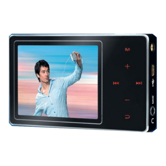
Chapter Two Functions and Operation Instructions 2.1 QUICK OPERATION 2.1.1 BUTTONS AND JACKS ILLUSTRATION V3 video: Push in power-off state power on Push for long in power-on state power off Push in playing interface pause/play switch Push when recording pause recording Push when tuning mute Push when timing with stopwatch... -
Page 10: Power On/Off
Press when in tuning search state auto search Press for long when in tuning search state Automanual search Press when in "My sound effect setting" select the frequency that you want to set Press when browsing picture switch pictures #Press when browsing e-book turn pages Press when in menu operation move cursor... -
Page 11: Video
After pressing button to exit from on-line menu, pictures will be played in the means of slide. PRESS 2.1.6 E-BOOK BROWSING After entering "E-book" item, press CAUTION: button to select text file and press button to #When the length of song's full path name is too browse e-book. -
Page 12: Tuning
CAUTION: #In order to avoid sudden power-off in the course of recording, you cannot record when battery is low and when disc is fully written; if recording is in process, it indicates “FULL DISC” and exits from recording. This player adopts lithium-ion battery to #When recording with microphone, if you press supply power. -
Page 13: Playing Interface
8. Playback progress bar player may be used as mobile storage after drive program is being installed (please download it 2.2.3 RECORDING INTERFACE from BBK official website). ILLUSTRATION Connect MP3 player and computer with USB transmission line. After the bottom right corner of desktop appears “... -
Page 14: Disconnect Usb Safely
When in playing state, files cannot be cancelled. before use, please download video conversion tool and installation program “BBK MINIMP4 2.3.5 PLAY MUSIC conversion tool” from BBK website and then #PLAY MUSIC install to computer. In “music”, press button to select song, 2. -
Page 15: A-B Repeat Function
Probably lead to incorrect display. When playing 2.3.9 EQ MODE non-standard songs or songs with special format, The corresponding icons of each EQ mode noise may probably occur. in playback interface are shown as follows: 2.3.6 A-B REPEAT FUNCTION NORMAL JAZZ When playing, if you want to listen to content CLASSIC... -
Page 16: Record
2.3.12 RECORD #Preset In preset mode, pressing button may In main menu, after selecting “REC”, press adjust to the next channel and pressing button to enter recording ready state. In button may adjust to the previous channel. recording ready state, press button to pop up #Save on-line menu. -
Page 17: Calendar
After setup finishes, press button to confirm. #Calendar #Save bookmark Press button to enter "Calendar" setup. In on-line menu, select “Save bookmark” item button to set date. and press button to enter. Pressing button #Stopwatch may select th position to save and pressing In "Stopwatch"... -
Page 18: Brightness
2.4.8 FIRMWARE UPGRADING different formats. # Firmware upgrading #Screen saver function is not available when in This player supports firmware upgrading. video playing, stopwatch, Ebook and pictures. Please refer to the description on BBK website 2.4.4 BRIGHTNESS for details. #Brightness CAUTION: Press... -
Page 19: Chapter Three Principle And Servicing
Chapter Three Principle and Servicing Section One Principle of the Player 3.1.1 Block diagram of the player Block diagram of the player is shown in the picture 3.1.1.1: FLASH MEMORY SDRAM QVGA LCD LDO CIRCUIT POWER TPS79333 MANAGEMENT DC-DC CIRCUIT MODULE TPS62200 LDO BACKLIGHT... -
Page 20: Introduction To Ic Used By The Player
2. Power supply part: composed of lithium battery, TPS79333, TPS62200 and XC6206, which is responsible for power supply circuit of each part of the entire MP3. 3. Peripheral jack” composed of headphone output port, MIC input port and USB jack. Headphone jack is the audio output jack of the player, MIC is the audio input jack of external recording and USB jack fulfills internal and external data exchange of the machine to realize charge function. - Page 21 SSD1928QL9 LCD drive RT9284B 12V voltage DC-DC conversion TPS79333DBVR 3.3V voltage DC-DC conversion TPS62200 1.8V voltage DC-DC conversion MCP73832 Charge management XC6206P152MR 1.8V voltage stabilizing CSTCR4M00G55 SMD ceramic resonance CY8C21534 Touch button control - 16 -...
-
Page 22: Section Two Unit Circuit Principle
Section Two Unit Circuit Principle 3.2.1 Video decode circuit principle 1. Video decode circuit is mainly composed of main decode chip Rk2608, SDRAM and peripheral circuit. Rk2608 may realize video file decode playing of MPEG-4 format in low frequency and power consumption with clear and smooth picture quality, meanwhile, Rk2608 integrates large amount of I/O control jacks which may provide the max flexibility. -
Page 23: Audio Decode Circuit Principle
2. Working principle: when the machine power on, reset circuit keeps high level reset signal. After RK2608 completes reset through reset pin 113, reset signals output from pin 56 to pin 42 of SSD1928 to enable SSD1928 to finish reset (V3 screen need no SSD1928 drive, so there is no this reset process), at the same time reset signals are sent to enable end of RT9284, boost circuit begins to work and screen is lightened. -
Page 24: Flash Circuit
When machine is in FM state, FM digital audio signals input from INPUT pin (pin 27, 28) of WM8750, after digital filtering and echo processing inside WM8750, and then output to headphone jack directly. 3.2.3 FLASH circuit 1. FLASH circuit schematic diagram is shown in the figure 3.2.3.1: RES# I/O7 R/B2... -
Page 25: Fm Tuning Circuit
There is firmware of the player’s working inside Flash and all tasks are completed by CPU to send out relevant order after the data exchange between CPU and Flash. When the player power on, 3.3V voltage supplies power for Flash through VCC, /CE inputs 3.3V high level signal and Flash begins to work effectively. -
Page 26: Display Screen Boost Circuit
When MP3 player switches in FM tuning state, antenna is sent to the RF band-pass filter (87.6MHz~108MHz and 76MHz 87.5MHz) composed of Li6, C57 and C59 through C56 coupling and then to pin 35, 37 of TEA5767 for amplifying through TEA5767 inside. Pin 2, 3, 4 of TEA5767 is connected with the internal VCO and with variant diode D10, D11 externally. -
Page 27: Usb Jack Circuit
reaches 750mA, the internal switch of RT9284 turns off, and supplies power for the rear circuit through external diode D3 at the same time when switch is off until feedback voltage is lower than reference voltage again. As for this PFM peak current control scheme adopted by convertor and discontinuous conduction means (DCM), the frequency depends on output current and makes the frequency of entire load very high. -
Page 28: Headphone Output Jack Circuit
3.2.7 Headphone output jack circuit 1. Headphone output jack circuit principle diagram is shown in the picture 3.2.7.1: OUT_R1 OUT_L1 C31 220UF/4V HP_OUTR 601/0603 HP_OUTL 601/0603 C32 220UF/4V 2SJ-A382-001(HP-DC) R102 R100 FM_ANT 601/0603 RCLAMP0504F/SC-70 Figure 3.2.7.1 Headphone output jack circuit 2. -
Page 29: Charge Management Circuit
Each button is actually a capacitor. When pressing this flat capacitor, it means two capacitors are connected parallel on two ends of this capacitor to make the capacitance of this capacitor become large charge/discharge cycle become long and the counting number for recording charge process become large. -
Page 30: Battery Voltage Detect Circuit
1000V PROG From the above, charge current is 400mA. When power adapter or USB is connected externally, input voltage is 5V; internal oscillator begins to oscillate; internal timer begins to time; charger begins to charge and IC automatically fulfills a complete charge process. -
Page 31: Battery Protection Circuit
3.2.11 Battery protection circuit 1. Battery protection board is installed on Li battery and used to prevent Li battery from being damaged by short-circuit, over-charge and over-discharge. Li battery and battery protection board are called as Li battery components. Battery protection board principle diagram is shown in the picture 3.2.11.1: Figure 3.2.11.1 Battery protection circuit 2. -
Page 32: Reset Circuit
CDRH3D16-100 240K 1% 47PF TPS62200/FAN5307* SOT23-5 106/X5R 106/X5R P_GND P_GND 100K 1% 390K 1% D_GND V_ADJ MMST3904 D_GND D_GND Figure 3.2.12.2 1.8V power circuit diagram 2. Working principle: seen from the circuit diagram, 3.3V power is supplied by IC TPS79333 and peripheral circuit. -
Page 33: Power On/Off Control Circuit
2. Working principle: when the player power on, voltage stabilizing circuit begins to work and 3.3V voltage VCC outputs. Voltage on two sends of capacitor C19 cannot change suddenly, so B electrode of triode Q3 is low level, Q3 is in cutoff state, RESETN is high level to reset for Rk2608 and display screen. Meanwhile, VCC charges capacitor C19. -
Page 34: Mic Circuit
When the time of pressing PLAY button is more than 1 second but less than 4 seconds, pin 57 of Rk2608 detects he change of voltage; software decides this signal is power-off signal and then saves contents of machine; pin 58 outputs high level, D12 is on to make Q7 on, VCC is grounded through CE electrode of Q7, enable end EN is low level, TPS62200 and TPS79333 stop voltage output and the player realizes software power-off. -
Page 35: Section Three Servicing Cases
Section Three Servicing Cases 3.3.1 Servicing cases [ Example 1 ] Symptom: power not on. Description: no OSD and no output. Analysis and troubleshooting: firstly confirm whether it is caused by battery or power circuit. Connect with computer and check whether display screen has display. Power on, connect and there is no display. - Page 36 [ Example 4 ] Symptom: noise when tuning. Description: radio station has noise when tuning. Analysis and troubleshooting: firstly judge whether the tuning components or common part has trouble. Listen to radio station by using headphone and check whether only one side of headphone has sound and the result is normal.
- Page 37 Analysis and troubleshooting: when power on, machine down before entering main menu. Press PLAY button to power on, when screen appears BBK picture justly, image of the player halts and button has no function. Firstly test power supply 3.3V, 3.8V and it normal. Then test crystal oscillator oscillation frequency and it is normal, so we judge that data has abnormality.
-
Page 38: Troubleshooting Diagram
3.3.2 Troubleshooting diagram 1. Troubleshooting flow chart for “No OSD” is shown in the picture 3.3.2.1: No OSD Whether Check DC-DC boost circuit D3 anode 12V voltage and peripheral elements is normal Whether there is 12V Check whether display screen voltage on display flat cable holderhas false welding screensocket... - Page 39 2. Troubleshooting flow chart for “USB is not connected” is shown in the picture 3.3.2.2: USB is not connected Check whether 5V Q2 has trouble or USB of Q2 is grounded socket has rosin joint normally Check whether 3.3V Check each DC-DC switch and 1.8V are normal circuit and peripheral elements Check...
- Page 40 3. Troubleshooting fow chart for “Do not charge” is shown in the picture 3.3.2.3: Do not charge Whether Check battery is fully whether USB_VBUS charge with voltage Check power supply circuit has 5V voltage 4.2V-4.3V Battery Whether is fully charged, BAT voltage has Change IC ISL6294 then protection...
- Page 41 4. Troubleshooting flow chart for "Power not on" is shown in the picture 3.3.2.4: Power not on Whether battery Whether there is OSD voltage is lower than Change battery components after connecting with 3.4V computer Whether battery Whether U16 input voltageis up to 3.6V Check D5 and Q2 Check charge circuit...
- Page 42 5. Troubleshooting flow chart for “Machine not power on” is shown in the picture 3.3.2.5: Machine not power on Whether Whether software upgrading 3.3V, 1.8V voltage output is available after connecting with computer is normal Whether Whether it is normal Change the main decode crystal oscillator Y1 Change crystal oscillator...
-
Page 43: Section Four Signal Waveform Diagram
Section Four Signal waveform diagram This section collects signal waveform diagram of audio, video and each unit circuit with the purpose To help servicing personnel to judge where trouble lies in accurately and quickly to improve servicing skills. For the difference of oscillograph's type, model and tuner, a certain difference may exist, so the servicing personnel are expected to pay more attention to check in daily operation. - Page 44 3. VCC waveform diagram 4. Display screen background light BCLK waveform diagram 5. PLAY1 waveform diagram when playing. - 39 -...
- Page 45 6. OUT_R waveform diagram when playing musical files. 7. OUT_L waveform diagram when playing musical files. 8. Crystal oscillator Y1 waveform diagram - 40 -...
- Page 46 9. U6 DC-DC switch waveform diagram 10. Power-on reset RESETN waveform diagram 11. Crystal oscillator XT1 waveform diagram - 41 -...
-
Page 47: Section Five Function Introduction To Ic
Section Five Function Introduction to IC 3.5.1 Function introduction to HY57V641620E 1. Description The Hynix HY57V641620E(L/S)T(P) series is a 67,108,864bit CMOS Synchronous DRAM, ideally suited for the memory applications which require wide data I/O and high bandwidth. HY57V641620E (L/S)T(P) is organized as 4banks of 1,048,576x16. HY57V641620E(L/S)T(P) is offering fully synchronous operation referenced to a positive edge of the clock. -
Page 48: Function Introduction To Rk2608
3. PIN Description SYMBOL TYPE DESCRIPTION The system clock input. All other inputs are registered to the SDRAM on the Clock rising edge of CLK Controls internal clock signal and when deactivated, the SDRAM will be one Clock Enable of the states among power down, suspend or self refresh Chip Select Enables or disables all inputs except CLK, CKE, UDQM and LDQM Selects bank to be activated during RAS activity Selects bank to be... - Page 49 ・ 56K words Program Sync SRAM ・ 48K words Data Sync SRAM ・ 2K words Register Space for Peripherals ・ Upgradable firmware through USB/Flash interface ◆ Memory interface: ・ External up to 4(cs) x 64M-4G bytes Nand type Flash accessed by DMA ・...
- Page 50 Flash/ LCD/ SDRAM data bus bit 4 I/O Pull up Flash/ LCD/ SDRAM data bus bit 5 I/O Pull up Flash/ LCD/ SDRAM data bus bit 6 I/O Pull up Flash/ LCD/ SDRAM data bus bit 7 I/O Pull up Flash ready/busy signal RD/BY I, Pull up...
- Page 51 P2.13/PWM0 GPIO/ PWM output0 SD/MMC Data output, Rock2 as input Connect to SD/MMC SDDO P2.0/SDDO SD/MMC Data input, Rock2 as output Connect to SD/MMC SDDI P2.1/SDDI P2.2/SDCLK SD/MMC Clock output P2.3/SDCS SD/MMC chip select output I/O POWER(3.3V) Digital Ground VSSD Digital Core power(1.8V) GPIO, External int0 P0.0...
- Page 52 L-channel single ended analog output VSSAO Negative power supply to output amplifiers Common mode analog output AOMS Common mode sense input VDDAO Positive power supply to output amplifiers R-channel single ended analog output HP_SENSE Sense of jack insertion Digital Core power(1.8V) I/O POWER(3.3V) Digital Ground VSSD...
-
Page 53: Function Introduction To Rt9284B
Crystal 24MHz OSC input PAD I, OSC XOUT O, OSC Crystal 24MHz OSC output PAD Digital Core power(1.8V) Digital Ground VSSD I/O POWER(3.3V) RESET I, Pull up System reset pin, low enable TEST I, Pull down Test mode, ( Internal 100K pull down) P1.0/ NORCSN I/O Pull up &... -
Page 54: Function Introduction To Tps62200
◆ Dimming with Zero-inrush and Wide Frequency Range of 100 to 100kHz ◆ Over Voltage Protection ◆ Output Current up to 100mA at VOUT = 12V. ◆ Zero Shutdown Supply Current ◆ Minimize the External Component ◆ Small LC Filter ◆... -
Page 55: Function Introduction To Mcp73832
◆ Adjustable Output Voltage Range From 0.7 V to VI ◆ Fixed Output Voltage Options Available ◆ Up to 300 mA Output Current ◆ 1 MHz Fixed Frequency PWM Operation ◆ Highest Efficiency Over Wide Load Current Range Due to Power Save Mode ◆... -
Page 56: Function Introduction To Tea5767Hn
◆ Linear Charge Management Controller: ・ Integrated Pass Transistor ・ Integrated Current Sense ・ Reverse Discharge Protection ◆ High Accuracy Preset Voltage Regulation: + 0.75% ◆ Four Voltage Regulation Options: ・ 4.20V, 4.35V, 4.40V, 4.50V ◆ Programmable Charge Current ◆ Selectable Preconditioning ◆... - Page 57 ◆ Crystal reference frequency oscillator; the oscillator operates with a 32.768 kHz clock crystal or with a 13 MHz crystal and with an externally applied 6.5 MHz reference frequency ◆ PLL synthesizer tuning system ◆ I2C-bus and 3-wire bus, selectable via pin BUSMODE ◆...
-
Page 58: Function Introduction To M41T62
XTAL2 crystal oscillator input 2 PHASEFIL phase detector loop filter PILFIL pilot detector low-pass filter n.c. not connected n.c. not connected VAFL left audio frequency output voltage VAFR right audio frequency output voltage TMUTE time constant for soft mute MPXO FM demodulator MPX signal output Vref reference voltage... - Page 59 Functions available to the user include a time-of-day clock/calendar, Alarm interrupts (M41T62/65), 32KHz output (M41T64), programmable Square Wave output (M41T62/63/64), and Watchdog output (M41T63/65). The eight clock address locations contain the century, year, month, date, day, hour, minute, second and tenths/hundredths of a second in 24 hour BCD format. Corrections for 28-, 29- (leap year), 30- and 31-day months are made automatically.
-
Page 60: Function Introduction To Wm8750Bl
Supply voltage 3.5.8 Function introduction to WM8750BL 1. Description The WM8750L is a low power, high quality stereo CODEC designed for portable digital audio applications. The device integrates complete interfaces to stereo or mono microphones and a stereo headphone. External component requirements are drastically reduced as no separate microphone or headphone amplifiers are required. - Page 61 ・Analogue 1.8V to 3.6V ・Digital core: 1.42V to 3.6V ・Digital I/O: 1.8V to 3.6V ◆ 256fs / 384fs or USB master clock rates: 12MHz, 24MHz ◆ Audio sample rates: 8, 11.025, 16, 22.05, 24, 32, 44.1, 48, 88.2, 96kHz generated internally from master clock ◆...
-
Page 62: Function Introduction To Xc6206P152Mr
LINPUT2 Analogue Input Left Channel Input 2 RINPUT1 Analogue Input Right Channel Input 1 LINPUT1 Analogue Input Left Channel Input 1 MODE Digital Input Control Interface Selection Digital Input Chip Select / Device Address Selection SDIN Digital Input/Output Control Interface Data Input / 2-wire Acknowledge output SCLK Digital Input Control Interface Clock Input... -
Page 63: Chapter Four Assembly And Disassembly Process
Chapter Four Assembly and Disassembly Process In order to get to know the structure of V3more easily and directly, now we use pictures to present each key point of disassembly and assembly process before all users to prevent users from operating blindly and to damage elements, so we hope you can operate according to the instructions strictly. - Page 64 5. Insert the 4 special slice clasp instruments 6. Use the special hook tool, shown in the into the relevant position of the 4 clasps. picture,to remove the middle casing. 7. Remove FPC flat cable clasp and then use 8. Use electric screwdriver or “+”-shaped forceps to take out FPC flat cable.
-
Page 65: Assembly Process Of The Player
11. Take out battery components. 12. Take out the stainless steel cover board on rear side of display screen. 13. Take out display screen components from the direction shown in the picture 4.2 Assembly process of the player Assembly process of the player is similar with the disassembly process, and only the sequence is reverse. -
Page 66: Chapter Cinque Pcb Board & Circuit Diagram
Chapter Cinque PCB board & Circuit diagram Section One PCB board 5.1.1 Surface layer of Main Board - 61 -... -
Page 67: Bottom Layer Of Main Board
5.1.2 Bottom layer of Main Board - 62 -... -
Page 68: Section Two Circuit Diagram
FM_3V3 C56 101 C57 27PF FM_ANT FM_ANT O603CS 120nH MURATA 47PF COILCRAFT TOKO SMD LLQ1608-AR10G 475/X5R FSGND FSGND FSGND FM_3V3 FSGND FSGND 100K O603CS 33nH±2% FSGND MURATA BB202 COILCRAFT OR TOKO SMD CPOP DIFL2 LLQ1608-A33NG VCOT1 DIFL1 C67 333 VCOT2 TCIFC FSGND VCOVCC... - Page 69 OUT_R1 OUT_L1 DBVDD C31 220UF/4V 601/0603 HP_OUTR 106/X5R WM8750 601 DCR<350mΩ 601/0603 HP_OUTL DBVDD LINPUT2 DCVDD RINPUT2 C32 220UF/4V 2SJ-A382-001(HP-DC) LINPUT3 AVDD RINPUT3 R100 HPVDD D_GND DGND MCLK# MCLK HPGND BCLK AGND ADCLRC ADCLRC D_GND DACLRC DACLRC R102 BCLK SPEAKER_OUTL DACDAT DACDAT LOUT2...
- Page 70 虾牛 BATT HY57V641620ETP Á ?8825598 XOUT 24MHz D 15 VDDQ VSSQ 20PF/NPO 20PF/NPO 100K±1% D 14 D 13 R17 100K±1% D_GND VSSQ VDDQ D 12 D 11 VDDQ VSSQ 100K D 10 D_GND VSSQ VDDQ 106/X5R DQM0 DQM0 W EN DQM1 DQM1 C ASN...
- Page 71 VOUT BYPASS 106/X5R TPS79333DBVR SOT23-5 106/X5R P_GND P_GND P_GND P_GND CDRH3D16-100 100k 240K±1% 47PF TPS62200/FAN5307* SOT23-5 PLAY/PAUSE 106/X5R 106/X5R BAT43WS USB_VBUS USB_VBUS P_GND P_GND 100K±1% 1N4148WS 390K±1% PLAY D_GND START D_GND V_ADJ 100R MMST3904 601 DCR<350mΩ SFI0402-050E100NP SI2305DS SOT23 P_GND R101 D_GND P_GND...
- Page 72 BAT43WS USB_VBUS CDRH3D16-100 USB_VBUS 240K±1% 47PF TPS62200/FAN5307* SOT23-5 106/X5R 106/X5R P_GND P_GND 100K±1% 390K±1% D_GND D_GND V_ADJ MMST3904 1N4148WS D_GND USB_VBUS 330K SFI0402-050E100NP P_GND...
-
Page 73: Chapter Six Bom List
ECH8601 TSSOP TRANSISTOR SMD FIELD EFFECT ① 0790090 ECH8601R TSSOP U2 TRANSISTOR 0882570 S-8261AANMG22 SO23-6 1633305 E29-0 V3N video(RU)B SILVER FPC BOARD 5449972 1633812 9 3-1 ② 0700186 SMD RADIATION DIODE 1SB0602V22D0CA01 D1,D3 ② 0700187 SMD RADIATION DIODE LTST-S270KRKT RED D1,D3 ... - Page 74 MATERIAL MATERIAL NAME SPECIFICATIONS LOCATION CODE 0090390 SMD RESISTOR 1/16W 18K±5% 0402 0090396 SMD RESISTOR 1/16W 33K±5% 0402 0090400 SMD RESISTOR 1/16W 47K±5% 0402 R6,R35,R36,R40,R46,R48,R57,R58,R82,R95 0090404 SMD RESISTOR 1/16W 68K±5% 0402 0090408 SMD RESISTOR 1/16W 100K±5% 0402 R18,R64,R70,R85,R94,R78 0090421 SMD RESISTOR 1/16W 330K±5% 0402 R86,R87,R92 0090433...
- Page 75 MATERIAL MATERIAL NAME SPECIFICATIONS LOCATION CODE C1,C2,C7,C14,C30,C50,C51,C52,C53,C54,C99 0310776 SMD CAPACITOR 6.3V 105±20% 5R 0402 ? ? ④ C1,C2,C7,C14,C30,C50,C51,C52,C53,C54,C99 0310662 SMD CAPACITOR 6.3V 105±10% 5R 0402 ④ 0310753 SMD CAPACITOR 16V 104±20% 5R 0402 0310717 SMD CAPACITOR 6.3V 475±20% 5R 0603 C60,C87,C96 C15,C16,C20,C35,C45,C48,C69,C79,C81,C83, 0310827...
- Page 76 MATERIAL MATERIAL NAME SPECIFICATIONS LOCATION CODE 0882850 4162 QFN ⑥ 0883330 WM8750BL QFN ⑥ 0883403 WM8750L QFN U11 ⑦ 0883193 R2608 LQFP U2 ⑦ 0883442 RK2608A LQFP U2 08825598 HY57V641620ETP-7 TSOP$ 0882388 TE5767HN HVQFN 0882476 TP62200 SO23-5 ⑧ 1090080 ESD ELEMENT RCL0504 SC70-6L ⑧...
-
Page 77: Chapter Seven V5 Assembly And Disassembly Process
Chapter Four V5 Assembly and Disassembly Process In order to get to know the structure of V5more easily and directly, now we use pictures to present each key point of disassembly and assembly process before all users to prevent users from operating blindly and to damage elements, so we hope you can operate according to the instructions strictly. -
Page 78: Assembly Process Of The Player
5. Separate the bottom casing and the middle casing. 6. Remove the clasp of button flat cable and then pull out button flat cable. 7. Take out 2 screws of main board. 8. Take out the main board from middle casing. 10. -
Page 79: Chapter Eight V5 Pcb Board & Circuit Diagram
Chapter Eight V5 PCB board & Circuit diagram Section One PCB board 8.1.1 Surface layer of Main Board - 74 -... -
Page 80: Bottom Layer Of Main Board
8.1.2 Bottom layer of Main Board - 75 -... -
Page 81: Section Two Circuit Diagram
OUT_R OUT_L FCM1608-601 T02 4V 220uF±20% 3528(B) HP_OUTL FCM1608-601 T02 4V 220uF±20% 3528(B) HP_OUTR 2SJ-0890-A02 HPOUT R120 R121 FM_ANT C126 C127 3.3V FCM1608-601 T02 FCM1608-601 T02 C124 RCLAMP0504F/SC-70 6L 16V 104 ±20% X5R 0402 6.3V106±20% X5R 0805 WM8750 D_GND DBVDD LINPUT2 DCVDD RINPUT2... - Page 82 3.3V 1.8V BATT D_GND 100K±1% XOUT D_GND 100K±1% D_GND 50V 20P±5% NPO 0402 50V 20P±5% NPO 0402 100K 24MHz D_GND D_GND 3.3V 6.3V106±20% X5R 0805 3.3V 6.3V106±20% X5R 0805 16V 104 ±20% X5R 0402 D_GND D_GND HY57V641620ETP D 15 RREF AGND VDDQ VSSQ...
- Page 83 FM_3V3 FM_ANT 50V 27P±5% NPO 0402 FM_ANT 50V 101±5% NPO 0402 120nH±2% 1608 25V 472 ?0% X7R 0402 50V 47P±5% NPO 0402 6.3V 475±20% X5R 0603 SGND 10V 473±10% X5R 0402 SGND FM_3V3 10V 473±10% X5R 0402 SGND R48 0R O603CS 100K MURATA...
- Page 84 3.3V 1928IOVDD 600Ω/100MHZ ?5% 1005 1.8V 1928PVDD 1928COREVDD 3.3V A027DL01/A030DL01 320*240(RGB) 16V 104 ±20% X5R 0402 16V 104 ±20% X5R 0402 16V 104 ±20% X5R 0402 6.3V106±20% X5R 0805 D_GND D_GND D_GND TFT_RST 1/16W 4.7K±5% 0402 3.3V TFT_SEN TFT_SCL TFT_SDA 3 .3V TFT_PVDD TFT_AVDD...
- Page 85 4.2V 3.3V 3.3V VOUT C108 C109 BYPASS 6.3V106±20% X5R 0805 6.3V106±20% X5R 0805 C110 TPS79333DBVR SOT23-5 D_GND 25V 103±10% X7R 0402 C111 D_GND 25V 102±10% X7R 0402 D_GND 1.8V 3.3V 10uH ±20% CDRH3D16/HP 1.8V C114 C113 C112 6.3V106±20% X5R 0805 240K±1% 6.3V106±20% X5R 0805 100k...
Need help?
Do you have a question about the V3N and is the answer not in the manual?
Questions and answers