Table of Contents
Advertisement
Quick Links
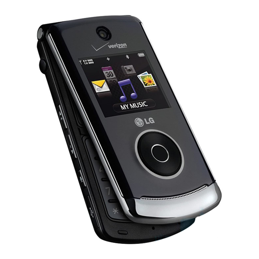
VX8560
Features of VX8560
1. Wave Type
● CELLULAR : G7W
● PCS: G7W
2. Frequency Scope
Transmit Frequency (MHz)
CELLULAR
824.82 ~ 848.19
3. Rated Output Power : CELLULAR = 0.25W
4. Output Conversion Method : This is possible by correcting the key board channel.
5. Voltage and Current Value of Termination Part Amplifier (Catalogue included)
MODE
CELLULAR
PCS
6. Functions of Major Semi-Conductors
Classification
QSC6075
Memory MCP
(H8BCS0SI0MAP-56M)
DSP (TCC8322)
MOVINAND Memory
(KMAFE0000A)
7. Frequency Stability
● CELLULAR : ±0.5PPM
● PCS : ±0.1PPM
LG Electronics Inc.
PCS
CELLULAR
1850~1910
869.82~893.19
PCS = 0.25W
Part Name
Voltage
ACPM7353
4.2V
ACPM7353
4.2V
Terminal operation control and digital signal processing
Flash Memory (2G) + SDRAM (1G)
Storing of terminal operation program
Digital signal processing
Flash Memory (1G)
Storing of user data (MP3 , Picture etc..)
Receive Frequency (MHz)
PCS
1930~1990
Current
Power
450mA
0.25W
460mA
0.25W
Function
GPS
1575.42
1/235
Advertisement
Table of Contents

Related Manuals for LG VX8560


Summary of Contents for LG VX8560
- Page 1 VX8560 Features of VX8560 1. Wave Type ● CELLULAR : G7W ● PCS: G7W 2. Frequency Scope Transmit Frequency (MHz) Receive Frequency (MHz) CELLULAR CELLULAR 824.82 ~ 848.19 1850~1910 869.82~893.19 1930~1990 1575.42 3. Rated Output Power : CELLULAR = 0.25W PCS = 0.25W...
- Page 2 VX8560 CDMA Mobile Subscriber Unit VX8560 SERVICE MANUAL SERVICE MANUAL DUAL BAND CDMA [PCS/Cellular/GPS] CDMA MOBILE PHONE LG Electronics Inc. 2/235...
- Page 3 ………………………………………………………………….…165 APPENDIX 1. Block Diagram ………………………………………………………………………178 2. Circuit diagram……………………………………………………………………...179 3. Component Layout…………………………………………………………………190 4. Assembly and Disassembly diagram…………………………………………...199 5. Part List………………………………………………………………………………202 6. BGA PIN MAP……………………………………………………………………….215 7. Accessories…………………………………………………………………………222 - AC adaptor……………………………………………………………………..223 - Cigar Light Charger…………………………………………………………..230 - USB Cable……………………………………………………………………...233 LG Electronics Inc. 3/235...
- Page 4 Cellular uses 800MHz and PCS uses 1.9GHz. The VX8560 support GPS Mode, we usually call it tri-band phone. Also, VX8560 works on Advanced Mobile Phone Service (S-GPS). We call it dual- mode phone. If one of the Cellular, PCS base stations is located nearby, Call fail rate of triple-mode phone is less than dual-mode phone or single-mode phone.
-
Page 5: Cdma Abstract
At this time, the spectrums of other signals that have different codes are not recovered into its original state, and appears as the self-interference of the system. LG Electronics Inc. 5/235... -
Page 6: Features And Advantages Of Cdma Mobile Phone
1.25msec (800 times per second). By doing so, the gain tolerance and the different radio propagation loss on the forward/backward link are complemented. LG Electronics Inc. 6/235... - Page 7 That is, each mobile station signal generates interference in relation to the signals of all the other mobile stations. LG Electronics Inc. 7/235...
- Page 8 In addition, in the CDMA system, services and service charges are classified further into different classes so that more transmit power can be allocated to high class service users for easier call set-up; they can also be given higher priority of using hand-off function than the general users. LG Electronics Inc. 8/235...
-
Page 9: Structure And Functions Of Tri-Band Cdma Mobile Phone
(AGC Amp). Then, they are converted into RF band by the frequency synthesizer synchronizing these signals to proper output frequencies. Transmit signals obtained pass through the duplexer filter and then, are sent out to the cell site via the antenna. LG Electronics Inc. 9/235... -
Page 10: Specification
4.1.10 Battery Type, Capacity and Operating Time. Unit = Hours : Minutes Standard (800mAh) CELLULAR About 165 Hours (SCI=2) Standby Time About 165 Hours (SCI=2) CELLULAR 160 Minutes (-92dBm input) Talk time 160 Minutes (-92dBm input) LG Electronics Inc. 10/235... -
Page 11: Transmit Specification
CELLULAR : 0.224W PCS: 0.224W 4.3.3 Interference Rejection Single Tone : -30dBm at 900 kHz (CELLULAR), -30dBm at 1.25MHz(PCS) Two Tone : -43dBm at 900 kHz & 1700kHz(CELLULAR), -43dBm at 1.25 MHz & 2.05 MHz (PCS) LG Electronics Inc. 11/235... - Page 12 Ch # Center Freq Ch # Center Freq Ch # Center Freq (MHz) (MHz) (MHz) 1851.25 1871.25 1891.25 1852.50 1872.50 1892.50 1853.75 1873.75 1893.75 1855.00 1875.00 1895.00 1856.25 1876.25 1896.25 1857.50 1877.50 1897.50 1858.75 1878.75 1898.75 LG Electronics Inc. 12/235...
- Page 13 Center Freq Ch # (MHz) (MHz) (MHz) 1931.25 1951.25 1971.25 1932.50 1952.50 1972.50 1933.75 1953.75 1973.75 1935.00 1955.00 1975.00 1936.25 1956.25 1976.25 1937.50 1957.50 1977.50 1938.75 1958.75 1978.75 1940.00 1960.00 1000 1980.00 1941.25 1961.25 1025 1981.25 LG Electronics Inc. 13/235...
- Page 14 1947.50 1967.50 1150 1987.50 1948.75 1968.75 1175 1988.75 4.5.3 GPS mode : 1575.42 MHz 4.5.4 Bluetooth mode : 2400 MHz ~ 2483.5 MHz 4.6 AC Adaptor : See Appendix 4.7 Cigar Lighter Charger : See Appendix LG Electronics Inc. 14/235...
-
Page 15: Installation
Clip the IB into the IB bracket. 5.3.4. Microphone Installation Install the microphone either by clipping I onto the sunvisor (driver’s side) or by attaching it to door post (driver’s side), using a velcro adhesive tape (not included). 5.3.5 Cable Connections LG Electronics Inc. 15/235... - Page 16 Connect the kit’s power cable connector to the interface box power receptacle. 5.3.5.2 Antenna Cable Connection Connect the antenna coupler cable connector from the cradle to the external antenna connector. ( Antenna is not included.) LG Electronics Inc. 16/235...
- Page 17 1)NAM Programming Method 1.Press ‘##77647268560” Rress “SEND” Enter Service code “000000” 2. Press ‘1’ key for entering ‘Service Prg.’ ● Usually pressing ‘Soft Key 1’ will save the change. ● To exit Service Program, press ‘END’ key. LG Electronics Inc. 17/235...
- Page 18 Press ‘ok’ Key to edit more NAM1 items. Press ‘Exit’ Key to exit Service Programming’ 2-2) NAM1 Phone Number (MDN) You can edit NAM1 Phone Number(MDN). Press ‘ok’ Key to edit more NAM1 items. Press ‘Back’ Key to edit previous NAM1 items. LG Electronics Inc. 18/235...
- Page 19 Press ‘ok’ Key to edit more NAM1 items. Press ‘Back’ Key to edit previous NAM1 items. 2-4) NAM1 Home SID You can edit NAM1 Home SID. Press ‘ok’ Key to edit more NAM1 items. Press ‘Back’ Key to edit previous NAM1 items. LG Electronics Inc. 19/235...
- Page 20 Press ‘Back’ Key 2 to edit previous NAM1 items. 2-6) More NAM1 Programming You can decide to edit more NAM1 items. Press ‘Exit’ Key to exit Service Programming. Press ‘More’ Key to edit more advanced NAM1 items. LG Electronics Inc. 20/235...
- Page 21 Press ‘OK’ Key to edit more NAM1 items. Press ‘Back’ Key to edit previous NAM1 items. 2-8) NAM1 MCC You can edit NAM1 Mobile Country Code. Press ‘OK’ Key to edit more NAM1 items. Press ‘Back’ Key to edit previous NAM1 items. LG Electronics Inc. 21/235...
- Page 22 Press ‘Back’ Key 2’ to edit previous NAM1 items. 2-10) NAM1 True IMSI MCC You can edit NAM1 True IMSI MCC. Press ‘OK’ Key to edit more NAM1 items. Press ‘Back’ Key to edit previous NAM1 items. LG Electronics Inc. 22/235...
- Page 23 Press ‘Back’ Key to edit previous NAM1 items. 2-12) NAM1 PRL Enabled You can see NAM1 PRL Enabled. Press ‘Soft Key 1’ to edit more NAM1 items. Press ‘Soft Key 2’ to edit previous NAM1 items. LG Electronics Inc. 23/235...
- Page 24 Press ‘Back’ Key to edit previous NAM1 items. 2-14) NAM1 CDMA Pri. CH A You can edit NAM1 CDMA Primary Channel A. Press ‘OK’ Key to edit more NAM1 items. Press ‘Back’ Key to edit previous NAM1 items. LG Electronics Inc. 24/235...
- Page 25 Press ‘Back’ Key to edit previous NAM1 items 2-16) NAM1 CDMA Pri. CH B You can edit NAM1 CDMA Primary Channel B. Press ‘OK’ Key to edit more NAM1 items. Press ‘Back’ Key to edit previous NAM1 items LG Electronics Inc. 25/235...
- Page 26 Press ‘OK’ Key to edit more NAM1 items. Press ‘Back’ Key to edit previous NAM1 items 2-18) Lockout SID/NID You can edit Lockout SID/NID Pairs. Press ‘OK’ Key to edit more NAM1 items. Press ‘Back’ Key to edit previous NAM1 items LG Electronics Inc. 26/235...
- Page 27 2-20) NAM1 Forn SID Reg You can edit NAM1 Foreign SID Registration. Press ‘OK’ Key to edit more NAM1 items. Press ‘Back’ Key to edit previous NAM1 items Press Left, Right, Up, Down key to toggle Yes/No. LG Electronics Inc. 27/235...
- Page 28 Press Left, Right, Up, Down key to toggle Yes/No. 2-22) NAM1 Acc Ovld Class You can see NAM1 Access Overload Class. Press ‘OK’ Key to edit more NAM1 items. Press ‘Back’ Key to edit previous NAM1 items LG Electronics Inc. 28/235...
- Page 29 Press ‘Edit’ Key to skip NAM2 items settings. Press ‘OK’ Key to edit NAM2 related items. 2-24) Phone Model You can see the Phone Model number. Press ‘OK’ Key to edit more NAM1 items. Press ‘Back’ Key to edit previous NAM1 items LG Electronics Inc. 29/235...
- Page 30 VX8560 2-25) Slot Cycle Index You can edit Slot Cycle Index Press ‘OK’ Key to edit more NAM1 items. Press ‘Back’ Key to edit previous NAM1 items 2-26) Powering Down Restart. LG Electronics Inc. 30/235...
-
Page 31: Chapter 3. Circuit Description
After that, the RF signal is amplified by the Power Amp in order to have enough power for radiation. Finally, the RF signal is sent out to the cell site via the antenna after going through the coupler and quintplexer. LG Electronics Inc. 31/235... - Page 32 VX8560 [Figure 1-1] RF Block Diagram of VX8560 LG Electronics Inc. 32/235...
- Page 33 The main function of quintplexer is to prohibit the other band signals from flowing into the one band circuit and vice versa. RF designer can use common tri-band antenna regardless of frequency band (800, 1575 and 1900 MHz). The specification of VX8560 quintplexer is described below: LG Electronics Inc.
- Page 34 VX8560 LG Electronics Inc. 34/235...
- Page 35 VX8560 LG Electronics Inc. 35/235...
- Page 36 The frequency selectivity characteristic of mobile phone is mostly determined by LNA. The specification of LG-VX8560 LNAs are described below: 1.2.2.1 Cellular CDMA LNA performance specifications LG Electronics Inc.
- Page 37 The characteristics of Low Noise Amplifier (LNA) are low noise figure, high gain, high intercept point and high reverse isolation. The frequency selectivity characteristic of mobile phone is mostly determined by LNA. The specification of LG-VX8560 GPS LNA is described below LG Electronics Inc.
- Page 38 The I/Q down converter outputs the CDMA signals at baseband frequency. Low-pass filtering enables the receiver to select the desired baseband signals from the effects of unwanted noise or adjacent-channel interference. I/Q base band components are converted to digital signals by two identical 4-bit ADCs. LG Electronics Inc. 38/235...
- Page 39 Tx VCO. The Tx IF signal is amplified by AGC controlled by QSC6055. The second mixer on RFT converts IF signals into RF signals. After passing through the upconverter , RF signal is inputted into the Power Amplifier Module. 1.3.1.1 Cellular CDMA transmit signal path performance specifications LG Electronics Inc. 39/235...
- Page 40 MMIC. The maximum power that can be inputted through the input terminal is +10dBm and conversion gain is about 28dB. RF transmit signals that have been amplified through the power amplifier are sent to the quintplexer. LG Electronics Inc. 40/235...
- Page 41 -30~+85 C. The receives frequency tuning signals called TRK_LO_ADJ from QSC6055 as 0.5V~2.5V DC via R and C filter in order to generate the reference frequency of 19.2MHz and input it into the frequency synthesizer of UHF band. Frequency stability depending on temperature is ±2.0 ppm. LG Electronics Inc. 41/235...
-
Page 42: Digital/Voice Processing Part
The memory part is made up of a MCP and MOVINAND for storing data. 2.2.5 Power Supply Part The power supply part is made up of circuits for generating various types of power, used for the digital/voice processing part. LG Electronics Inc. 42/235... - Page 43 VX8560 [Figure 2-2] Block Diagram of Digital/Voice Processing Part LG Electronics Inc. 43/235...
- Page 44 When received, I and Q data are demodulated into symbols by the demodulator, and then de-interleaved in reverse to the case of transmission. Then, the errors of data received from viterbi decoder are detected and corrected. They are voice-decoded at the vocoder in order to output digital voice data. LG Electronics Inc. 44/235...
-
Page 45: Memory Part
The ARM926 EJS microprocessor includes a 3 stage pipelined RISC architecture, both 32-bit ARM and 16-bit THUMB instruction sets, a 32-bit address bus, and a 32-bit internal data bus. It has a high performance and low power consumption. LG Electronics Inc. 45/235... - Page 46 LEDs and backlight circuitry are included in the keypad for easy operation in the dark. LCD MODULE LCD module contains a controller which will display the information onto the LCD by 16-bit data from the QSC6075. LG Electronics Inc. 46/235...
- Page 47 It supports I2S audio data format between DSP and codec. A speaker amplifier, using digital amplifier system, realizes low power consumption than that of linear amplifier. In addition, power-down mode is available to minimize the current consumption when used. LG Electronics Inc. 47/235...
-
Page 48: Chapter 4. Trouble Shooting
- Sect or Power: - 30 dB m Spec trum An alyzer Setting Os c illos c op e Setting 3. Check RF Signal path 1. Check DC Power Supply circuit Redownload S/W, Cal 2. Check VCTCXO LG Electronics Inc. 48/235... -
Page 49: Test Point
VX8560 4.1.1.1 Checking DC Power supply circuit (PMIC) Test Point Test Point TP1:R207 + 2.6V_MSMP TP2:R202 + 2.1V_RFRX1 TP3:R208 + 2.1V_RFRX2 Circuit Diagram Circuit Diagram LG Electronics Inc. 49/235... - Page 50 Refer to Logic troubleshoot Check R207 The Proble m may be Lo gic part +2.6V_MSMP is OK? Refer to Logic troubles hoot DC Po wer supply Circuit is OK. See next Page to c hec k VCTCXO circuit LG Electronics Inc. 50/235...
-
Page 51: Checking Vctcxo Circuit
VX8560 4.1.1.2 Checking VCTCXO circuit Test Point Test Point TP1 : X101 pin3 TP2 : X101 pin4 Circuit Diagram Circuit Diagram LG Electronics Inc. 51/235... - Page 52 Replace X 101 and then check C115 , R 105 . VCTCXO circuit is Ok . See next page Is it similar? to check control signal . Replace Main B /D Waveform Waveform Figure 4.1.1 (a) Figure 4.1.1 (b) LG Electronics Inc. 52/235...
- Page 53 VX8560 4.1.1.3 Checking RF signal path (Mobile S/W, Quintplexer) Test Point Test Point Quintplexer Mobile S/W VCTCXO QSC6075 LG Electronics Inc. 53/235...
- Page 54 VX8560 PCS Tx Circuit Diagram Circuit Diagram DCN Tx PCS Rx DCN Rx LG Electronics Inc. 54/235...
- Page 55 To Figure 4.1.1 (d ). Is any signal detected at that point? Is any signal detected at Check L113, C124 that point? All DCN Rx check is completed . If the phone still do not work , change Main B /D . LG Electronics Inc. 55/235...
- Page 56 VX8560 Waveform Waveform U100 pin2 4.1.1 (c) DP100 pin1 4.1.1 (d) LG Electronics Inc. 56/235...
- Page 57 - Sect or Power: - 30 dB m Spec trum An alyzer Setting Os c illos c op e Setting 3. Check RF Signal path 1. Check DC Power Supply circuit Redownload S/W, Cal 2. Check VCTCXO LG Electronics Inc. 57/235...
- Page 58 VX8560 4.1.2.1 Checking DC Power supply circuit (PMIC) Test Point Test Point TP1:R207 + 2.6V_MSMP TP2:R202 + 2.1V_RFRX1 TP3:R208 + 2.1V_RFRX2 Circuit Diagram Circuit Diagram LG Electronics Inc. 58/235...
- Page 59 Refer to Logic troubleshoot Check R207 The Proble m may be Lo gic part +2.6V_MSMP is OK? Refer to Logic troubles hoot DC Po wer supply Circuit is OK. See next Page to c hec k VCTCXO circuit LG Electronics Inc. 59/235...
- Page 60 VX8560 4.1.2.2 Checking VCTCXO circuit Test Point Test Point TP1 : X101 pin3 TP2 : X101 pin4 Circuit Diagram Circuit Diagram LG Electronics Inc. 60/235...
- Page 61 Replace X 101 and then check C115 , R 105 . VCTCXO circuit is Ok . See next page Is it similar? to check control signal . Replace Main B /D Waveform Waveform Figure 4.1.2 (a) Figure 4.1.2 (b) LG Electronics Inc. 61/235...
- Page 62 VX8560 4.1.2.3 Checking RF signal path (Mobile S/W, Quintplexer) Test Point Test Point Quintplexer Mobile S/W VCTCXO QSC6075 LG Electronics Inc. 62/235...
- Page 63 VX8560 PCS Tx Circuit Diagram Circuit Diagram DCN Tx PCS Rx DCN Rx LG Electronics Inc. 63/235...
- Page 64 To Figure 4.1.2 (d ). Is any signal detected at that point? Is any signal detected at Check L114, L116, C125 that point? All PCS Rx check is completed . If the phone still do not work , change Main B /D . LG Electronics Inc. 64/235...
- Page 65 VX8560 Waveform Waveform U100 pin2 4.1.2 (c) DP100 pin2 4.1.2 (d) LG Electronics Inc. 65/235...
- Page 66 - Measure frequency domain waveform with Spectrum analyser - Measure time domain waveform with Oscilloscope 6. Check Quintplexer 1. Check DC Power Supply circuit 7. Check Mobile Switch 2. Check VCTCXO Redownload S/W, Cal 3. Check QSC6075 LG Electronics Inc. 66/235...
- Page 67 VX8560 4.2.1.1 Checking DC Power supply circuit (PMIC) Test Point Test Point TP1:R207 + 2.6V_MSMP TP2:R209 + 2.1V_RFTX Circuit Diagram Circuit Diagram LG Electronics Inc. 67/235...
- Page 68 +2.1V_RFTX is OK? Refer to Logic troubleshoot Check R207 The Problem may be Lo gic part +2.6V_MSMP is OK? Refer to Logic troubleshoot DC Po wer supply Circuit is OK. See next Page to check VCTCXO circuit LG Electronics Inc. 68/235...
- Page 69 VX8560 4.2.1.2 Checking VCTCXO circuit Test Point Test Point TP1 : X101 pin3 TP2 : X101 pin4 Circuit Diagram Circuit Diagram LG Electronics Inc. 69/235...
- Page 70 Replace X 101 and then check C115 , R 105 . VCTCXO circuit is Ok . See next page Is it similar? to check control signal . Replace Main B /D Waveform Waveform Figure 4.2.1 (a) Figure 4.2.1 (b) LG Electronics Inc. 70/235...
- Page 71 VX8560 4.2.1.3 Checking QSC6075 circuit Test Point Test Point CELL_OUT TP1: C162 U200 QSC6075 Circuit Diagram Circuit Diagram LG Electronics Inc. 71/235...
- Page 72 Checking Flow Start Check pinK23 at U200 (C162) Check if there is any major difference referring QSC 6075 is OK . See next page To Figure 4.2.1.3. Is it similar? Replace U200 Waveform Waveform Graph 4.2.1.3 LG Electronics Inc. 72/235...
- Page 73 Checking Flow Waveform Checking Flow Waveform Start RF_IN fed up with CW signal Check pin9, at F105 . Referring to RF_OUT RF Tx SAW is OK Figure 4.2.1.4. Is it similar? Replace F 105 Figure 4.2.1.4 LG Electronics Inc. 73/235...
- Page 74 VX8560 4.2.1.5 Check DCN PAM circuit Test Point Test Point U106 VEN_DCN VCC2 VCC1 VMODE RFIN_CELL RFOUT_CELL Circuit Diagram Circuit Diagram PCS Tx DCN Tx LG Electronics Inc. 74/235...
- Page 75 2.2V. Check pin3 at U106(PA _RANGE) Check PA_RANGE whether it is lower than 2.2V. Replace U106 Waveform Waveform RF_IN fed up with CW signal in low gain mode of PAM RF_IN RF_OUT Figure 4.2.1.5 LG Electronics Inc. 75/235...
- Page 76 VX8560 4.2.1.6 Check Quintplexer Test Point Test Point Ant Port DCN Port DP100 LG Electronics Inc. 76/235...
- Page 77 VX8560 PCS Tx Circuit Diagram Circuit Diagram DCN Tx PCS Rx DCN Rx LG Electronics Inc. 77/235...
- Page 78 VX8560 Checking Flow Checking Flow Start Check pin3, 5 at DP100. Referring to Quintplexer is OK Figure 4.2.1.6. Is it similar? Replace DP 100 Waveform Waveform DCN Port ANT Port Figure 4.2.1.6 LG Electronics Inc. 78/235...
- Page 79 Circuit Diagram RF IN RF OUT Checking Flow Waveform Checking Flow Waveform Start RF IN Check pin1, 2 at U100. Referring to Mobile S /W is Figure 4.2.1.7. Is it similar? Replace U100 RF OUT Figure 4.2.1.7 LG Electronics Inc. 79/235...
- Page 80 - Measure frequency domain waveform with Spectrum analyser - Measure time domain waveform with Oscilloscope 6. Check Quintplexer 1. Check DC Power Supply circuit 7. Check Mobile Switch 2. Check VCTCXO Redownload S/W, Cal 3. Check QSC 6075 LG Electronics Inc. 80/235...
- Page 81 VX8560 4.2.2.1 Checking DC Power supply circuit (PMIC) Test Point Test Point TP1:R207 + 2.6V_MSMP TP2:R209 + 2.1V_RFTX Circuit Diagram Circuit Diagram LG Electronics Inc. 81/235...
- Page 82 +2.1V_RFTX is OK? Refer to Logic troubleshoot Check R207 The Problem may be Lo gic part +2.6V_MSMP is OK? Refer to Logic troubleshoot DC Po wer supply Circuit is OK. See next Page to check VCTCXO circuit LG Electronics Inc. 82/235...
- Page 83 VX8560 4.2.2.2 Checking VCTCXO circuit Test Point Test Point TP1 : X101 pin3 TP2 : X101 pin4 Circuit Diagram Circuit Diagram LG Electronics Inc. 83/235...
- Page 84 Replace X 101 and then check C115 , R 105 . VCTCXO circuit is Ok . See next page Is it similar? to check control signal . Replace Main B /D Waveform Waveform Figure 4.2.2 (a) Figure 4.2.2 (b) LG Electronics Inc. 84/235...
- Page 85 VX8560 4.2.2.3 Checking QSC6075 circuit Test Point Test Point CELL_OUT TP1: C162 U200 QSC6075 Circuit Diagram Circuit Diagram LG Electronics Inc. 85/235...
- Page 86 Checking Flow Start Check pinN23 at U200 (C161) Check if there is any major difference referring QSC 6075 is OK . See next page To Figure 4.2. 2.3. Is it similar? Replace U200 Waveform Waveform Graph 4.2.2.3 LG Electronics Inc. 86/235...
- Page 87 Checking Flow Waveform Checking Flow Waveform Start RF_IN fed up with CW signal Check pin6, at F105 . Referring to RF_OUT RF Tx SAW is OK Figure 4.2.2.4. Is it similar? Replace F 105 Figure 4.2.2.4 LG Electronics Inc. 87/235...
- Page 88 VX8560 4.2.2.5 Check PCS PAM circuit Test Point Test Point RFOUT_PCS RFIN_PCS VEN_PCS U106 VCC2 VCC1 VMODE Circuit Diagram Circuit Diagram PCS Tx DCN Tx LG Electronics Inc. 88/235...
- Page 89 2.2V. Check pin3 at U106(PA _RANGE) Check PA_RANGE whether it is lower than 2.2V. Replace U106 Waveform Waveform RF_IN fed up with CW signal in low gain mode of PAM RF_OUT Figure 4.2.2.5 LG Electronics Inc. 89/235...
- Page 90 VX8560 4.2.2.6 Check Quintplexer Test Point Test Point Ant Port DCN Port DP100 LG Electronics Inc. 90/235...
- Page 91 VX8560 PCS Tx Circuit Diagram Circuit Diagram DCN Tx PCS Rx DCN Rx LG Electronics Inc. 91/235...
- Page 92 VX8560 Checking Flow Checking Flow Start Check pin3, 5 at DP100. Referring to Quintplexer is OK Figure 4.2.1.6. Is it similar? Replace DP 100 Waveform Waveform DCN Port ANT Port Figure 4.2.1.6 LG Electronics Inc. 92/235...
- Page 93 Circuit Diagram RF IN RF OUT Checking Flow Waveform Checking Flow Waveform Start RF IN Check pin1, 2 at U100. Referring to Mobile S /W is Figure 4.2.2.7. Is it similar? Replace U100 RF OUT Figure 4.2.2.7 LG Electronics Inc. 93/235...
-
Page 94: Power On Trouble
Logic level at PS _ HOLD(CON200)_ and try again of U200 High ? Does it work properly ? Does it work properly Re-download software and try again Re-download software and try again The Phone will power on LG Electronics Inc. 94/235... - Page 95 VX8560 Circuit Diagram Circuit Diagram R707 PWR_ON_SW/ L200 +1.3_MSMC C263 +1.8_MSME1 C259 +2.6_MSMP C267 +2.1_MSMA C239 +2.8_TCXO CON200 PS_HOLD LG Electronics Inc. 95/235...
- Page 96 VX8560 Test point Test point R707 PWR_ON_SW/ L200 +1.3_MSMC C263 +1.8_MSME1 C259 +2.6_MSMP C267 +2.1_MSMA C239 +2.8_TCXO CON200 PS_HOLD LG Electronics Inc. 96/235...
- Page 97 VX8560 Circuit Diagram Circuit Diagram PIN4 OF U400 V_CHAR PIN4 OF CON300 VBAT LG Electronics Inc. 97/235...
-
Page 98: Charging Trouble
Voltage of pin4 CON300 Check the soldering VBATT(+VPWR) Replace Q300 Re-solder CON300 The battery may have the problem. Is the battery charged ? Change the battery and try again. Charging will operate properly LG Electronics Inc. 98/235... - Page 99 VX8560 Test point Test point PIN4 OF U400 V_CHAR PIN4 OF CON300 VBAT LG Electronics Inc. 99/235...
- Page 100 4.3.2.1 DSP Trouble Checking Flow Checking Flow START Check the voltage of the Sub PMIC Replace U608 +1.2V_DSP_CORE +2.6V_DSP_SDRAM +2.6V_DSP_IO Check DSP Clock at C505 Replace U511 Check the control signal Replace U510 TP512~520 DSP will operate properly LG Electronics Inc. 100/235...
- Page 101 VX8560 Circuit Diagram Circuit Diagram L606 +1.2V_DSP_CORE C636 +2.6V_DSP_SDRAM C641 +2.6V_DSP_IO LG Electronics Inc. 101/235...
- Page 102 VX8560 PIN3 OF U511 LG Electronics Inc. 102/235...
- Page 103 VX8560 TP512 DSP_TDI TP513 DSP_TMS TP515 DSP_TDO TP516 NTRST TP517 DSP_TCK TP518 DSP_RTCK TP519 TP10 NRESET TP520 TP11 JTAG_DSP_RESET LG Electronics Inc. 103/235...
- Page 104 VX8560 Test point Test point L606 +1.2V_DSP_CORE C636 +2.6V_DSP_SDRAM C641 +2.6V_DSP_IO LG Electronics Inc. 104/235...
- Page 105 VX8560 PIN3 OF U511 LG Electronics Inc. 105/235...
- Page 106 VX8560 TP512 DSP_TDI TP513 DSP_TMS TP515 DSP_TDO TP516 NTRST TP517 DSP_TCK TP518 DSP_RTCK TP519 TP10 NRESET TP520 TP11 JTAG_DSP_RESET LG Electronics Inc. 106/235...
-
Page 107: Lcd Trouble
Change the LCDModule Check the DSP Trouble(4.3.2) Replace U511 Check the Voltage of C703 =2.8V ? Replace U200 Check the Control singnal Data[0:15] Check F701,F702,F703,F704,F705 LCD_RESET/,LCD_CS/,LCD_WE/ Check CON105 soldering Replace FPCB On FPCB LCD display will work properly LG Electronics Inc. 107/235... - Page 108 VX8560 Circuit Diagram Circuit Diagram C703 +2.8V_LCD LG Electronics Inc. 108/235...
- Page 109 VX8560 C708 LCD_RESET/ F701 LCD_WE/,CS/ F702 LCD_D[0]~[3] F703 LCD_D[4]~[7] F704 LCD_D[8]~[11] F705 LCD_D[12]~[15] LG Electronics Inc. 109/235...
- Page 110 LCD_RESET/ F701 LCD_WE/,CS/ F702 LCD_D[0]~[3] F703 LCD_D[4]~[7] F704 LCD_D[8]~[11] F705 LCD_D[12]~[15] F702 F704 F701 F703 F705 LCD_ID LCD_D[0] LCD_D[4] LCD_D[8] LCD_D[12] SLCD_CS/ LCD_D[5] LCD_D[9] LCD_D[13] LCD_D[1] MLCD_CS/ LCD_D[6] LCD_D[10] LCD_D[14] LCD_D[2] LCD_WE/ LCD_D[3] LCD_D[7] LCD_D[11] LCD_D[15] LG Electronics Inc. 110/235...
-
Page 111: Camera Trouble
Check the clock from Camera Replace the Camera module at R722;CAM_PCLK Check the Voltage of the following LDOs:+1.5V_CAM_CORE, Replace U610,F708 +2.6V_CAM_IO,+2.8V_CAM_ANALOG Check the Control signal Check F706,F707,C722,C720,C721 CAM_DATA[0:7],CAM_RESET/, CAM_SDA,CAM_SCL Check CON103 on FPCB Replace FPCB Camera will work properly LG Electronics Inc. 111/235... - Page 112 VX8560 Circuit Diagram Circuit Diagram R722 CAM_PCLK LG Electronics Inc. 112/235...
- Page 113 VX8560 C658 +2.6V_CAM_IO C659 +1.5V_CAM_CORE C746 +2.8V_CAM_ANALOG LG Electronics Inc. 113/235...
- Page 114 VX8560 F706 CAM_D[0]~[3] F707 CAM_D[4]~[7] C720 CAM_SDA C721 CAM_SCL C722 CAM_RESET/ LG Electronics Inc. 114/235...
- Page 115 VX8560 Test point Test point R722 CAM_PCLK LG Electronics Inc. 115/235...
- Page 116 VX8560 C658 +2.6V_CAM_IO C659 +1.5V_CAM_CORE C746 +2.8V_CAM_ANALOG LG Electronics Inc. 116/235...
- Page 117 VX8560 Test point Test point U104 F706 CAM_D[0]~[3] F707 CAM_D[4]~[7] C720 CAM_SDA C721 CAM_SCL C722 CAM_RESET/ LG Electronics Inc. 117/235...
-
Page 118: Speaker Trouble
Check the clock at Check the clock signal at C122 Replace U200 C278 Check the signal Check the audio signal at SPK+,SPK- Replace U605 at R603,R604 Replace U602,U604 Check the state of speaker contact Speaker will work properly LG Electronics Inc. 118/235... - Page 119 VX8560 Circuit Diagram Circuit Diagram C606,C607 HPH_L,HPH_R C603 DBVDD(WM8900) C609 DCVDD(WM8900) C611 CPVDDH1(WM8900) C612 CPVDDH0(WM8900) C613 AVDD(WM8900) LG Electronics Inc. 119/235...
- Page 120 VX8560 C122 MCLK(WM8900) LG Electronics Inc. 120/235...
- Page 121 VX8560 C278 SLEEP X-TAL LG Electronics Inc. 121/235...
- Page 122 VX8560 R736 SPK_R- R737 TP10 SPK_R+ R738 TP11 SPK_L- R739 TP12 SPK_L+ LG Electronics Inc. 122/235...
- Page 123 VX8560 C617 LINEOUT_1R C619 TP10 LINEOUT_1L LG Electronics Inc. 123/235...
- Page 124 VX8560 Test point Test point C606,C607 HPH_L,HPH_R C603 DBVDD(WM8900) C609 DCVDD(WM8900) C611 CPVDDH1(WM8900) C612 CPVDDH0(WM8900) C613 AVDD(WM8900) LG Electronics Inc. 124/235...
- Page 125 VX8560 C122 MCLK(WM8900) LG Electronics Inc. 125/235...
- Page 126 VX8560 C278 SLEEP X-TAL LG Electronics Inc. 126/235...
- Page 127 VX8560 R736 SPK_R- R737 TP10 SPK_R+ R738 TP11 SPK_L- R739 TP12 SPK_L+ LG Electronics Inc. 127/235...
- Page 128 VX8560 C617 LINEOUT_1R C619 TP10 LINEOUT_1L LG Electronics Inc. 128/235...
-
Page 129: Receiver Trouble
VX8560 4.3.5.2 Receiver Trouble Checking Flow Checking Flow START Replace U200 Check the RCV+,RCV- Replace The Receiver Speaker will work properly LG Electronics Inc. 129/235... - Page 130 VX8560 Circuit Diagram Circuit Diagram C705 RCV+ C706 RCV- LG Electronics Inc. 130/235...
- Page 131 VX8560 Test point Test point C705 RCV+ C706 RCV- LG Electronics Inc. 131/235...
-
Page 132: Headset Trouble
? Set the audio part of the test equipment to continuous wave mode : Headset receiving Can you hear the Sound from headset ? path problem : Headset sending path problem Headset will work properly LG Electronics Inc. 132/235... - Page 133 VX8560 Checking Flow: Headset detect problem Checking Flow: Headset detect problem Check the voltage R640 Replace U200 whether its range is low ? Re-solder CON601 Check the soldering of CON601 Replace CON601 LG Electronics Inc. 133/235...
- Page 134 C645,C646 Re-solder C645,C646 Replace U605 Re-solder U200 Check the voltage at C603,C609, Check the audio signal at R611,R612 with heat gun C611,C612,C613 Replace U200 Resolder R605 Check the soldering of CON601 Re-solder CON601 Replace Main B/D LG Electronics Inc. 134/235...
- Page 135 Check the voltage at R646 Check the soldering of U609 Whether its range is 1.65~2.1V ? Re-solder U609 with heat gun Replace U609 Does it work ? Re-download S/W Does it work well ? Replace Main B/D LG Electronics Inc. 135/235...
- Page 136 VX8560 Circuit Diagram Circuit Diagram R640 EJACK_DETECT/ R611 LHP_EJ R612 RHP_EJ R646 TP13 EAR_MIC LG Electronics Inc. 136/235...
- Page 137 VX8560 C606 HPH_L C607 HPH_R C645 LHP_EJ C646 RHP_EJ C603 DBVDD(WM8900) C609 DCVDD(WM8900) C611 TP10 CPVDDH1(WM8900) C612 TP11 CPVDDH0(WM8900) C613 TP12 AVDD(WM8900) LG Electronics Inc. 137/235...
- Page 138 VX8560 Test point Test point R640 EJACK_DETECT/ R611 LHP_EJ R612 RHP_EJ R646 TP13 EAR_MIC LG Electronics Inc. 138/235...
- Page 139 VX8560 C606 HPH_L C607 HPH_R C645 LHP_EJ C646 RHP_EJ C603 DBVDD(WM8900) C609 DCVDD(WM8900) C611 TP10 CPVDDH1(WM8900) C612 TP11 CPVDDH0(WM8900) C613 TP12 AVDD(WM8900) LG Electronics Inc. 139/235...
- Page 140 Whether its range is 1.2~1.5V R238 Resolder R238 Resolder MIC Check the soldering at R620 Check the signal level at Resolder U606 Each side of MIC Check the soldering of MIC network Resolder MIC network (C281,C282) MIC will work properly LG Electronics Inc. 140/235...
-
Page 141: Mic Trouble
VX8560 4.3.5.4 MIC Trouble Circuit Diagram Circuit Diagram R238 MIC_BIAS C281 MIC1N C282 MIC+ LG Electronics Inc. 141/235... - Page 142 VX8560 R620 MIC_OUT+ C282 MIC+ C605 LINPUT1 LG Electronics Inc. 142/235...
- Page 143 VX8560 Test point Test point R238 MIC_BIAS C281 MIC1N C282 MIC+ LG Electronics Inc. 143/235...
- Page 144 VX8560 R620 MIC_OUT+ C282 :Refer to TP3 in Previous Page MIC+ C605 LINPUT1 LG Electronics Inc. 144/235...
- Page 145 START Is the voltage level of +VPWR Charge battery 3.3 ~ 4.2V? Check the soldering of each R andLEDS, Are all LEDs working ? or replace if not wor king Main key backlight will work properly LG Electronics Inc. 145/235...
- Page 146 VX8560 Circuit Diagram Circuit Diagram LED601 LED602 side lighting side lighting Test point Test point LED602 LED601 side lighting side lighting LG Electronics Inc. 146/235...
- Page 147 Setting: “ON” at the motor test of “test mode” Start Is the MOTOR_EN Hig? Replace U200 Resolder Check soldering R635,L607,L608,D602 R635,L607,L608,D602 Check soldering CON602 Replace CON602 Check the state at contact of vibrator Re-contact vibrator Replace Vibrator The vibrator will Work properly LG Electronics Inc. 147/235...
- Page 148 VX8560 Circuit Diagram Circuit Diagram L607 MOTOR_EN Test point Test point L607 MOTOR_EN LG Electronics Inc. 148/235...
- Page 149 Check the Voltage of C758 whether it is 2.6V Replace F709 Check the Signal at C707,C728. Is there any pulse when you rotate wheel key ? Replace FPCB Is the Wheel key work properly? Replace wheel key I Wheel key will work properly LG Electronics Inc. 149/235...
- Page 150 Replace Main PCB When you rotate wheel key ? Check the signal at pin 6, 7 of CON101 of FPCB, is there any pulse Replace FPCB When you press touch ? Touch key will work properly LG Electronics Inc. 150/235...
- Page 151 VX8560 Circuit Diagram Circuit Diagram C758 +2.6V_WHEEL C707 WHEEL_SENSE1 C728 WHEEL_SENSE2 LG Electronics Inc. 151/235...
- Page 152 VX8560 PIN36 OF CON703 WHEEL_SENSE1 PIN37 OF CON703 WHEEL_SENSE2 PIN6 OF CON101 WHEEL_SENSE1 PIN7 OF CON101 WHEEL_SENSE2 LG Electronics Inc. 152/235...
- Page 153 VX8560 Test point Test point C758 +2.6V_WHEEL C707 WHEEL_SENSE1 C728 WHEEL_SENSE2 LG Electronics Inc. 153/235...
- Page 154 VX8560 PIN36 OF CON703 WHEEL_SENSE1 PIN37 OF CON703 WHEEL_SENSE2 PIN6 OF CON101 WHEEL_SENSE1 PIN7 OF CON101 WHEEL_SENSE2 LG Electronics Inc. 154/235...
- Page 155 Check the clock at C141 Check the signal at TP110~114 Replace 200 Check the RF signal at C140 Replace U109 Check the RF signal at R114 Replace F103 Check soldering ANT103 Resolder ANT103 BT will work properly LG Electronics Inc. 155/235...
- Page 156 VX8560 Circuit Diagram Circuit Diagram C150 VDDO C144 VDDR3V,VREG1.. C141 VDDR3V,VREG1.. U110 BT_RESET/ U111 BT_MSM_DP_RFR/ U112 BT_MSM_DP_CTS/ U113 BT_MSM_DP_TXD U114 BT_MSM_DP_RXD C140 RFION R114 TP10 LG Electronics Inc. 156/235...
- Page 157 VX8560 Test point Test point C150 VDDO C144 VDDR3V,VREG1.. C141 VDDR3V,VREG1.. C140 RFION R114 TP10 LG Electronics Inc. 157/235...
- Page 158 VX8560 U104 U110 BT_RESET/ U111 BT_MSM_DP_RFR/ U112 BT_MSM_DP_CTS/ U113 BT_MSM_DP_TXD U114 BT_MSM_DP_RXD LG Electronics Inc. 158/235...
- Page 159 Check the signal of I2C at Replace U510 R637,R638 Check the I2S signal at Replace U510 R629,R630,R631 & FM_RESET at R602 Check the RF signal at C610 Replace U601 Check soldering ANT600 Resolder ANT600 FMT will work properly LG Electronics Inc. 159/235...
- Page 160 VX8560 Circuit Diagram Circuit Diagram C615 C614 R637 FM_SCL R638 FM_SDA R629 I2S_LRCK R630 I2S_DATA_OUT R631 I2S_BCLK R602 FM_RESET/ C610 LG Electronics Inc. 160/235...
- Page 161 VX8560 Test point Test point C615 C614 R637 FM_SCL R638 FM_SDA R629 I2S_LRCK R630 I2S_DATA_OUT R631 I2S_BCLK R602 FM_RESET/ C610 LG Electronics Inc. 161/235...
- Page 162 If so, use only a manufacture approves antenna. Otherwise, take your phone to a qualifies service center for repair. Use only the supplied or approved antenna. Non-approved antennas, modifications, or attachments, could impair call quality, damage the phone, and violate FCC regulations. LG Electronics Inc. 162/235...
- Page 163 LG Electronics Inc. 163/235...
- Page 164 Park, Quincy, MA 02269, Attn: Publication Sales Division. Rule of Thumb: Using common sense at all times when handling, installing or using the phone. Any questions should be directed to you nearest Service Center or authorized service technician or electrician. LG Electronics Inc. 164/235...
-
Page 165: Chapter 6. Glossary
A-key. A secret, 64-bit pattern stored in the mobile station. It is used to generate update the mobile station’s Shared Secret Data. The A-key is used in the mobile station authentication process. LG Electronics Inc. 165/235... - Page 166 Neighbor Set, and Remaining Set. . See Code Division Multiple Access CDMA Channel. The set of channels transmitted between the base station within a given CDMA frequency assignment. See also Forward CDMA Channel and Reverse CDMA Channel. LG Electronics Inc. 166/235...
- Page 167 Digital Color Code (DCC). A digital signal transmitted by a base station on a forward analog control channel that is used to detect capture of a base station by an interfering mobile station. Dim-and-Burst. A frame in which primary traffic is multiplexed with either secondary traffic or signaling traffic. LG Electronics Inc. 167/235...
- Page 168 Channels. The Forward CDMA Channel always carries a Pilot Channel and may carry up to one Sync Channel, up to seven Paging Channels, and up to 63 Traffic Channels, as long as the total number of channels, including the Pilot Channel, is no greater than 64. LG Electronics Inc. 168/235...
- Page 169 Layer 2. Layer 2 provides for the correct transmission and reception of signaling messages, including partial duplicate detection. See also Layering and Layer 3. Layer 3. Layer 3 provides the control of the Cellular telephone systems. Signaling messages originate and terminate at layer 3. See also Layering and Layer 2. LG Electronics Inc. 169/235...
- Page 170 Mobile Station Terminated Call. A call received by a mobile station (not to be confused with a disconnect or call release). Mobile Switching Center (MSC). A configuration of equipment that provides Cellular radiotelephone service. Also called the Mobile Telephone Switching Office (MTSO) LG Electronics Inc. 170/235...
- Page 171 OLC. See Overload Class (CDMA) or Overload Control (analog). Optional Field. A field defined within a message structure that is optionally to the message recipient. Order. A type of message that contains control codes for either the mobile station or the base station. LG Electronics Inc. 171/235...
- Page 172 CDMA Channel and the Reserve CDMA Channel. Different base station are identified by different pilot PN sequence offsets. Pilot PN Sequence Offset Index. The PN offset in units of 64 PN chips of a pilot, relative to the zero offset pilot PN sequence. LG Electronics Inc. 172/235...
- Page 173 Active Set, Candidate Set, and Neighbor Set. See also Active Set, Candidate Set, and Neighbor Set. Request. A layer 3 message generated by either the mobile station or the base station to retrieve information, ask for service, or command an action. LG Electronics Inc. 173/235...
- Page 174 Slot Cycle. A periodic interval at which a mobile station operating in the slotted monitors the Paging Channel. Slotted Mode. An operation mode of the mobile station in which the mobile station monitors only selected slots on the Paging Channel when in the Mobile Station Idle State. LG Electronics Inc. 174/235...
- Page 175 The counter is incremented an average of once per 80 ms period. Time Reference. A reference established by the mobile station that is synchronous with the earliest arriving multipath component used for demodulation. LG Electronics Inc. 175/235...
- Page 176 Walsh Function. One of 2N time orthogonal binary functions (note that the functions are orthogonal after mapping ‘0’ to 1 and ‘1’ to –1). Zone-Based Registration. An autonomous registration method in which the mobile station registers whenever it enters a zone that is not in the mobile station’s zone list. ㎲. Microsecond LG Electronics Inc. 176/235...
-
Page 177: Usb Cable
VX8560 Appendix Appendix Block Diagram Circuit diagram Component Layout Assembly and Disassembly diagram Part List BGA PIN MAP Accessories - AC adaptor - Cigar Light Charger - USB Cable LG Electronics Inc. 177/235... -
Page 178: Appendix 1. Block Diagram
VX8560 Appendix 1. Block Diagram Appendix 1. Block Diagram LG Electronics Inc. 178/235... -
Page 179: Appendix 2. Circuit Diagram
VX8560 Appendix 2. Circuit diagram Appendix 2. Circuit diagram 2- 1. Main PCB Circuit Diagram 2- 2. FPCB Circuit Diagram LG Electronics Inc. 179/235... -
Page 180: Main Pcb Circuit Diagram
VX8560 2-1. MAIN PCB CIRCUIT DIAGRAM 2-1. MAIN PCB CIRCUIT DIAGRAM LG Electronics Inc. 180/235... - Page 181 Doc. Name LG-VX8560 MAIN Doc. Number SAFY0258201 SHEET : 1 OF 7 DRAW : F102 ANT100 ANT101 ANT102 MIC94071 [Tx PART] DATE MAIN ANT VOUT 04/21/2008 +2.1V_RFTX +VPWR L102 CHKD G_SLUG C117 1005 2.2u C127 APRD C134 1608 2.2u S.H.KWAK...
- Page 182 LG-VX8560 Main Doc.Name Doc.Number SHEET SAFY0258201 DRAW S.J.CHANG DATE 04/21/2008 CHKD APRD S.H.KWAK LNA_OUT_C_HB LNA_OUT_C_HB UART1_RX_D BT_MSM_DP_RXD LNA_OUT_C_LB BT_MSM_DP_TXD LNA_OUT_C_LB UART1_TX_D MIX_INP_C_LB MIX_INP_C_LB GP_PDM_0/ETM_MODE_INT/GPIO_0 GATED_IOEN MIX_INM_C_LB MIX_INM_C_LB PA_ON1/GPIO_1 PA_ON1 MIX_INP_C_HB MIX_INP_C_HB SDCC_CMD/GPIO_2 BT_WAKEUP MIX_INM_C_HB SDCC_DATA0/GPIO_3 HOST_WAKEUP MIX_INM_C_HB ISSUE Rev.1.0 PWR_DET_IN...
- Page 183 Doc. Name LG-VX8560 MAIN Doc. Number SAFY0258201 SHEET : 3 OF 7 DRAW : S.J.CHANG DATE 04/21/2008 CHKD APRD S.H.KWAK ISSUE : Rev.1.0 MCP (2Gbit NAND FLASH + 1Gbit DDR SDRAM) BATTERY CONTACT CONTENT : Q300 NUS5530MN & Etc. V_CHAR...
- Page 184 Doc. Name LG-VX8560 MAIN Doc. Number SAFY0258201 SHEET : 4 OF 7 DRAW : S.J.CHANG DATE 04/21/2008 CHKD APRD S.H.KWAK MICRO USB RECEPTACLE SD SOCKET ISSUE : Rev.1.0 CONTENT : U400 NUS3065MUTAG Connector CON401 CNTRL GATE R403 49225-0821 & I/O...
- Page 185 Doc. Name LG-VX8560 MAIN Doc. Number SAFY0258201 SHEET : 5 OF 7 DRAW : S.J.CHANG DATE 04/21/2008 +2.6V_DSP_IO R530 +3.0V_DSP_SD +2.6V_MSMP CHKD R529 +1.8V_MSME1 +2.6V_DSP_SDRAM +1.2V_DSP_CORE +3.3V_DSP_USB APRD S.H.KWAK EBI2_A_D[2] TP508 EBI2_A_D[15] TP509 +1.8V_MSME1 +3.0V_MOVINAND U506 MOVINAND 1GBytes TC7SZ04FU ISSUE : Rev.1.0...
- Page 186 Doc. Name LG-VX8560 MAIN Doc. Number SAFY0258201 SHEET : 6 OF 7 DRAW : S.J.CHANG WOLFSON CODEC SPEAKER AMP. DATE 04/21/2008 R632 CHKD +VPWR TP602 TP601 U604 APRD YDA145 S.H.KWAK C619 1005 Sub PMIC R603 1005 OUT+ SPK_R+ C620 1005...
- Page 187 Doc. Name LG-VX8560 MAIN Doc. Number SAFY0258201 SHEET : 7 OF 7 F701 DRAW : S.J.CHANG ICVE10184E150R101FR MAIN TO FPCB BTB CONNECTOR (80) DATE LCD_ID OUT1 04/21/2008 SLCD_CS/ OUT2 CON703 CHKD MLCD_CS/ OUT3 AXK780147G LCD_WE/ OUT4 APRD S.H.KWAK ROW1 CAM_PWR_DOWN...
- Page 188 VX8560 2-2. FPCB CIRCUIT DIAGRAM 2-2. FPCB CIRCUIT DIAGRAM LG Electronics Inc. 188/235...
- Page 189 Doc. Name LG-VX8560 FPCB Doc. Number SACY0071101 SHEET : 1 OF 1 DRAW : DATE 04/21/2008 CHKD APRD S.H.KWAK CAMERA CONNECTOR LCD CONNECTOR ISSUE : Rev.1.0 CONTENT : CON105 AXT544124 CAM_D[7] FPCB CAM_D[6] LCD_D[0] LCD_D[8] CAM_D[5] LCD_D[1] LCD_D[9] CAM_D[4] LCD_D[2]...
-
Page 190: Appendix 3. Component Layout
VX8560 Appendix 3. Component Layout Appendix 3. Component Layout 3- 1. Main PCB Top 3- 2. Main PCB Bottom 3- 3. FPCB Top 3- 4. FPCB Bottom LG Electronics Inc. 190/235... - Page 191 VX8560 3-1. Main PCB Top Component Layout 3-1. Main PCB Top Component Layout LG Electronics Inc. 191/235...
- Page 192 U607 U607 cam5 FOLDER S/W C650 C651 EM-0781-T5 R719 U700 Photo Sensor APDS-9005-020 SW720 SW722 TP201 SW710 TP504 TP503 TP505 TP502 SW721 cam1 cam2 TP520 TP519 TP518 TP517 TP516 TP515 TP513 TP512 U111 U113 U112 U114 U110 U108 U107 cam4 cam3 LED602 LED601...
- Page 193 VX8560 3-2. Main PCB Bottom Component Layout 3-2. Main PCB Bottom Component Layout LG Electronics Inc. 193/235...
- Page 194 R611 C756 C738 R709 R735 C746 C722 C740 R711 R649 C616 U603 C658 C657 TP605 CON601 CON601 U609 U603 Earphone Jack U610 Comparator 7620-3_5G-DB1-A R646 NCS2200SQ2T2G R127 R129 R128 C752 C751 R640 C653 CON703 C660 U609 BTB Connector(80Pin) Dual SPDT AXK780147G NLAS3158MNR2G CON703...
- Page 195 VX8560 3-3. FPCB Top Component Layout 3-3. FPCB Top Component Layout LG Electronics Inc. 195/235...
- Page 196 CON103 CON106 Camera- Speaker- Connector(24pin) Connector(6pin) AXK7L24227G 04-6298-006-000-883 C102 CON101 Wheel- Connector(10pin) AXK7L10227G 196/235 CON101...
- Page 197 VX8560 3-4. FPCB Bottom Component Layout 3-4. FPCB Bottom Component Layout LG Electronics Inc. 197/235...
- Page 198 CON104 CON104 Connector(80pin) AXK880145WG CON105 CON105 LCD- Connector(44pin) AXT544124 R102 R125 C101 198/235...
-
Page 199: Appendix 4. Assembly And Disassembly Diagram
VX8560 Appendix 4. Assembly and Disassembly diagram Appendix 4. Assembly and Disassembly diagram LG Electronics Inc. 199/235... - Page 200 200/235...
- Page 201 201/235...
-
Page 202: Appendix 5. Part List
VX8560 Appendix 5. Part List Appendix 5. Part List 5- 1. Main PCB Part List 5- 2. FPCB Part List LG Electronics Inc. 202/235... -
Page 203: Main Pcb Part List
C 159 C A P ,C E R A M IC ,C H IP E C C H 0000701 1.2 pF,50V ,C ,N P 0 ,TC ,1005 ,R /TP C 1005C 0G 1H 1R 2C T LG Electronics Inc. 203/235... - Page 204 E C Z H 0 0 0 1 2 1 5 1 u F ,1 0 V ,K ,X 5 R ,T C ,1 0 0 5 ,R /T P C 1 0 0 5 X 5 R 1 A 1 0 5 K T LG Electronics Inc. 204/235...
- Page 205 S E V Y 0 0 0 5 1 0 1 1 8 V , ,S M D ,5 p F , 1 0 0 5 IC V L 0 5 1 8 0 5 0 F R LG Electronics Inc. 205/235...
- Page 206 E C C H 0 0 0 0 1 6 1 3 3 n F ,1 6 V ,K ,X 7 R ,H D ,1 0 0 5 ,R /T P M C H 1 5 3 C N 3 3 3 K K LG Electronics Inc. 206/235...
- Page 207 E C Z H 0 0 0 0 8 3 0 3 3 p F ,5 0 V ,J ,N P 0 ,T C ,1 0 0 5 ,R /T P C 1 0 0 5 C 0 G 1 H 3 3 0 JT LG Electronics Inc. 207/235...
- Page 208 E D T Y 0 0 0 9 4 0 1 V M N 2 ,5 V ,1 0 W ,R /T P ,1 .0 *0 .6 *0 .4 ,; , ,7 .8 2 V , , ,1 0 0 m WR S B 6 .8 C S T 2 R LG Electronics Inc.
- Page 209 LE D 602 D IO D E ,LE D ,C H IP E D LH 0013701 W H ITE ,E TC ,R /TP ,S ID E V IE W ,; ,[em pty] ,2.9~3.75 LE W W S 44P A LG Electronics Inc. 209/235...
- Page 210 R E S ,C H IP ,M A K E R E R H Z 0 00 02 38 20 0 K oh m ,1 /16 W ,F ,1 00 5 ,R /T P M C R 0 1M Z S F 20 03 LG Electronics Inc. 210/235...
- Page 211 E R H Y 0 0 0 9 5 2 6 4 .7 K o h m ,1 /2 0 W (0 .0 5 W ) ,J ,0 6 0 3 ,R /T P M C R 0 0 6 M Z P J4 7 2 LG Electronics Inc. 211/235...
- Page 212 C ou pler_ D C N T x ,; ,[e m p ty] ,8 36 .5 M H z ,2 5M H z L D C 1 58 36 M 2 0Q -3 60 LG Electronics Inc. 212/235...
- Page 213 19.2 M H z,1.5 P P M ,40 pF,S M D ,3.2*2.5*0.9 , ,; , ,1.5P P M X 101 V C TC X O E X S K 0005703 ,2.8V ,3.2 ,2.5 ,0.9 , ,S M D ,P /TP D S A 321S C E (19.2M ) LG Electronics Inc. 213/235...
- Page 214 S P C Y 0 1 3 3 3 0 1 P O L Y I ,.5 m m ,M U L T I-7 [B U IL D U P ] , ,; , , , , , , , , , S P C Y 0 1 3 3 3 0 1 LG Electronics Inc. 214/235...
-
Page 215: Appendix 6. Bga Pin Map
VX8560 Appendix 6. BGA Pin Map Appendix 6. BGA Pin Map 6- 1. U109 [BCM2046B1] 6- 2. U200 [QSC6075] 6- 3. U300 [H8BCS0SI0MAP 6- 4. U507 [KMAFE0000A] 6- 5. U510 [TCC8322] LG Electronics Inc. 215/235... - Page 216 VX8560 6-1. U109 [BCM2046B1] 6-1. U109 [BCM2046B1] USED PIN NOT USED PIN LG Electronics Inc. 216/235...
- Page 217 VX8560 6-2. U200 [QSC6075] 6-2. U200 [QSC6075] USED PIN NOT USED PIN LG Electronics Inc. 217/235...
- Page 218 VX8560 6-3. U300 [H8BCS0SI0MAP] 6-3. U300 [H8BCS0SI0MAP] USED USED LG Electronics Inc. 218/235...
- Page 219 VX8560 6-4. U507 [KMAFE0000A] 6-4. U507 [KMAFE0000A] USED PIN NOT USED PIN LG Electronics Inc. 219/235...
- Page 220 VX8560 6-5. U510 [TCC8322] 6-5. U510 [TCC8322] LG Electronics Inc. 220/235...
- Page 221 VX8560 6-5. U510 [TCC8322] 6-5. U510 [TCC8322] USED PIN NOT USED PIN LG Electronics Inc. 221/235...
-
Page 222: Appendix 7. Accessories
VX8560 Appendix 7. Accessories Appendix 7. Accessories 7- 1. AC adaptor 7- 2. Cigar Light Charger 7- 3. USB Cable LG Electronics Inc. 222/235... - Page 223 VX8560 7-1. AC adaptor 7-1. AC adaptor LG Electronics Inc. 223/235...
- Page 224 Allen Kwon Software revision: Fax #: 973-451-4325 Email: skwon@lge.com For phone model (list all applicable): Address: 55 Madison Ave. Suite #310, Morristown, VX8560, VX9700 NJ 07960 Other Descriptors: For Batteries Only Battery Pack Internal battery code: Cell Chemistry: Battery Pack Model:...
-
Page 225: Known Issues
Accessory Hardware & Software Release Notes Known Issues: Exceptions: Issues Resolved since Last Hardware/Software Version (Version #) Note: Do not delete past release notes information. Latest changes should be listed first. Date all releases). Special Testing Instructions: Proprietary & Confidential Subject to Non-Disclosure Obligations between VZW & Your Company Doc Rev 2 6/22/06 225/235... - Page 226 Allen Kwon Software revision: Fax #: 973-451-4325 Email: skwon@lge.com For phone model (list all applicable): Address: 55 Madison Ave. Suite #310, Morristown, VX8560, VX9700 NJ 07960 Other Descriptors: For Batteries Only Battery Pack Internal battery code: Cell Chemistry: Battery Pack Model:...
- Page 227 Accessory Hardware & Software Release Notes Known Issues: Exceptions: Issues Resolved since Last Hardware/Software Version (Version #) Note: Do not delete past release notes information. Latest changes should be listed first. Date all releases). Special Testing Instructions: Proprietary & Confidential Subject to Non-Disclosure Obligations between VZW & Your Company Doc Rev 2 6/22/06 227/235...
- Page 228 Allen Kwon Software revision: Fax #: 973-451-4325 Email: skwon@lge.com For phone model (list all applicable): Address: 55 Madison Ave. Suite #310, Morristown, VX8560, VX9700 NJ 07960 Other Descriptors: For Batteries Only Battery Pack Internal battery code: Cell Chemistry: Battery Pack Model:...
- Page 229 Accessory Hardware & Software Release Notes Known Issues: Exceptions: Issues Resolved since Last Hardware/Software Version (Version #) Note: Do not delete past release notes information. Latest changes should be listed first. Date all releases). Special Testing Instructions: Proprietary & Confidential Subject to Non-Disclosure Obligations between VZW & Your Company Doc Rev 2 6/22/06 229/235...
- Page 230 VX8560 7-2. Cigar Light Charger 7-2. Cigar Light Charger LG Electronics Inc. 230/235...
- Page 231 Allen Kwon Software revision: Fax #: 973-451-4350 Email: skwon@lge.com For phone model (list all applicable): Address: 55 Madison Ave. Suite #310, Morristown, VX8560, VX9700, VX8610 NJ 07960 Other Descriptors: N/A For Batteries Only Battery Pack Internal battery code: Cell Chemistry:...
- Page 232 Accessory Hardware & Software Release Notes Micro USB ID Register value add (180k, F) Micro USB Plug design change (VPC with ID Resistor) VPC without ID Res. VPC with ID Res. Exceptions: Issues Resolved since Last Hardware/Software Version (Version #) Note: Do not delete past release notes information.
- Page 233 VX8560 7-3. USB Cable 7-3. USB Cable LG Electronics Inc. 233/235...
- Page 234 Allen Kwon Software revision: Fax #: 973-451-4325 Email: skwon@lge.com For phone model (list all applicable): Address: : 55 Madison Ave. Suite #310, Morristown, VX8560, VX9100, VX9700 NJ 07960 Other Descriptors: For Batteries Only Battery Pack Internal battery code: Cell Chemistry: ...
- Page 235 Accessory Hardware & Software Release Notes Known Issues: Micro USB Data cable spec change Cable length Cable thickness Before 1.5m After 1.2m After drawing Exceptions: Micro USB ID Register value add (180k, F) 180KΩ Issues Resolved since Last Hardware/Software Version (Version #) Note: Do not delete past release notes information.
Need help?
Do you have a question about the VX8560 and is the answer not in the manual?
Questions and answers