Table of Contents
Advertisement
Advertisement
Table of Contents

Related Manuals for Fluke PM6685


Summary of Contents for Fluke PM6685
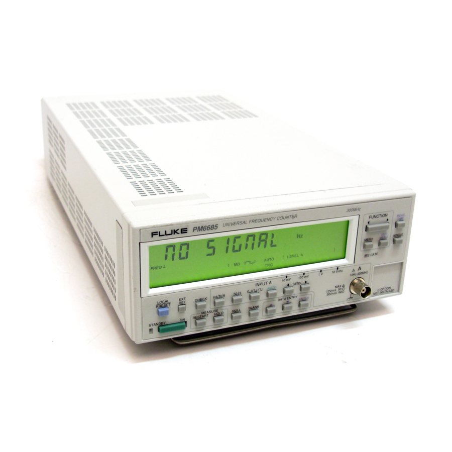
- Page 1 Programmable Frequency Counter PM6685 & PM6685R Service Manual...
- Page 2 This is a complementary service manual covering instruments with manufacturing numbers exceeding 840684. The principal differences are to be found in Chapter 7 and in Chapter 8 due to a major redesign of the main PCB. Do not dispose of the previous edition, identified by the part number, 4822 872 25012, and the publishing date, June 1996. You may have to refer to it for information on older instruments as well as options not mentioned here.
-
Page 3: Table Of Contents
Contents Safety Instructions General Directives......5-9 Performance Check Calibration Adjustments General Information ......2-2 Introduction . - Page 4 This page is intentionally left blank.
-
Page 5: Safety Instructions
Chapter 1 Safety Instructions... - Page 6 Authorized service and calibration of this instrument is available Power extension cables must always have a protective ground con- through your Fluke representative. See address at the end of this ductor. manual. Indicates that the operator should consult the manual.
-
Page 7: Performance Check
Chapter 2 Performance Check... -
Page 8: General Information
Enter the test menu by pressing the ENTER key. PM9691 & PM9692 PM6681R 10 MHz ±0.0001 Hz Fluke 910R or Ce - Selections for internal self-tests are: for PM6685R sium Standard 1 TEST ALL (Test 2 to 5 in sequence) HF signal genera - 0.5 GHz (no presc.) -
Page 9: Short Form Specification Test
Keyboard Test NOTE: For the instrument to respond correctly, this test must be carried out in sequence and you must start with the The keyboard test verifies that the counter responds when you press preset (power-on) setting. any key. To check the function behind the keys, see the tests further * The LSD may vary. -
Page 10: Rear Input/Output
EXT ARM INPUT – Connect the reference to input A. – Check the readout against the accuracy requirements of your – Press the PRESET key, then press the ENTER key to set your application. counter in the Default setting. – Select 50 W input impedance. -
Page 11: Options
Options Prescaler This extra HF input (PM9624) is easily recognized by its front panel connector (Input C, type N). EX T R E F Fig 2-2 Connect the output of the signal generator to the HF input of the counter. Required Test Equipment Suggested Specification HF signal generator... - Page 12 This page is intentionally left blank. 2-6 Performance Check, Options...
-
Page 13: Disassembly
Chapter 3 Disassembly... -
Page 14: Removing The Cover
- rated from all voltage sources. The PM6685 is available with a number of options and accessories. – The labels on the rear panel of the counter identify the options and Make sure the power cord is disconnected from the counter. -
Page 15: Pm9691 Or Pm9692 (Oven Oscillator)
PM9691 or PM9692 (Oven – When installing the HF input, make sure that the connector pins fit exactly in the holes in the connector housing (C). Oscillator) – Disconnect the power cable. – Remove the cover of the counter. – Remove the two screws (A) holding the oscillator to the main pca from underneath. - Page 16 This page is intentionally left blank. 3-4 Disassembly, PM9691 or PM9692 (Oven Oscillator)
-
Page 17: Circuit Descriptions
Chapter 4 Circuit Descriptions... -
Page 18: Block Diagram Description
Block Diagram Description General molded front unit is fixed to the two profiled aluminum rods with screws. The PM6685 Frequency Counter consists of three main units: The main board unit consists of a PCB mounted on two profiled alu- – Front unit minum rods. - Page 19 ASIC External reference Input Amplifier Micro- computer Gate LED Trigger DAC´s Display Local preset HSI.0 RESET Reset circuit Analog output Option 80 GPIB option Power supply +12V 90-265 V -5.2V Keyboard Fig. 4-1 PM6685 block diagram. Block Diagram Description 4-3...
-
Page 20: Hardware Functional Description
Hardware Functional Description Front Unit Keyboard U13A LCD Drivers Main Board Keyboard & Display Latch Board U 20 1 B ac k pl. 0 Dr iv er 1 AD0-AD7 H0-H3 Bac k pl. 1 P C F8 576 S CL LC D S y nc . -
Page 21: Main Board
selected if the relay is open. Depending on selected attenuation, the Main Board 1 MW input impedance is determined by different combinations of resistors. Introduction In x1 attenuation mode (K2 is closed and K3 is open) the impedance Components not necessary for explaining the function are omitted is determined by resistor network R22 to R28. - Page 22 Voltage limiter and D3 to clamp positive voltage and resistor R36 plus the diodes D2 and D4 to clamp negative voltage. The clamp voltage is approxi - mately ±2.1 V for low frequency signals. At high frequency the clamp voltage rises to approximately ±2.3 V. Impedance Converter Stage The analog signal from the input stage is fed to an amplifier stage where split-band technique is used to get good frequency response...
- Page 23 of transistor Q2. This point is common to the high and low frequency The trigger level circuits, which are described later, generate a DC paths. level in the range of approximately æ1.6 V. This covers a dynamic range of 6.4 V since the input signal is divided by a factor of 2 before A buffer amplifier with high driving capacity is used to get a linear it reaches the comparator.
- Page 24 approximately 2 times. The trigger level circuits generate a DC level The trigger level circuits consist of the following: that has the same attenuation. This means that the output of this cir - – Resistor network R57 to R68 for generating the reference volt - cuit has a range of –1.6 V to +1.6 V with a resolution of maximum ages 0.04 V, 0.22 V, 0.59 V, and 1.6 V.
- Page 25 tance is 15 Wwhen the resistor is cold but decreases to a few ohms as Power Supply it is warmed up by the steady-state current. General survey The AC voltage is rectified in the bridge rectifier D9 and filtered in The power supply generates four regulated DC supply voltages to the C64.
- Page 26 Therefore the power module will never be switched off. the OUTPUT connector. The level is fixed TTL. The PM6685 has consequently only a secondary power switch. A relay (K5) disconnects the load on the +5 V and –5.2 V at stand-by.
- Page 27 RE SET SYNC CNTS CY 1 CY 2 HODLYX HODLYX HOS X I NTB EXTC HODLYY HODLYY HOS Y I NTA BURST CLOCK CLOCK ST OP TOTSTA V CCO S TAARM ST ART GNDD1 STOARM GNDD2 STADLY GNDD3 STODLY GNDD4 TI ME Inter- M RE F...
- Page 28 units with facilities for coarse and fine adjustment. They are fixed to Keyboard Scanning the main PCB with two screws. The output signal is AC-coupled to U13A the X2 pin on U29 via C107. Main Board Keyboard & Display Latch Board External This input consists of an AC-coupled line receiver with Schmitt trig-...
-
Page 29: Rear Panel Unit
– The STAND-BY button is connected to the ON/STANDBY logic in the power supply. – The LOCAL/PRESET button is connected directly to input pin 24 on the microcontroller U11. Pressing this button sends an interrupt to a special handler in the SW. Rear Panel Unit The rear panel contains the following connectors INPUTS:... -
Page 30: Optional Units
Analog Out Optional Units The result on the display can be converted to an analog signal by means of a pulse-width-modulated (PWM) signal from the micro- GPIB Interface Including Analog Output processor. The signal is filtered, attenuated, offset-adjusted, inte- grated and buffered by IC103 and supporting passive components to GPIB, PM9626B give an analog DC level between 0 and 4.98 V with a resolution of 20 mV. -
Page 31: Software Functional Description
The basic structure of the main module is as follows: The PresetDevice procedure reprograms the complete device when the PRESET key has been pressed (in local mode). It aborts pending main PM6685() measurements. The ExecuteGpibCommands procedure executes GPIB commands Initialize();... -
Page 32: Test Routines
Test Routines Test Routines via AUX MENU Key The test routines are the routines accessible via the AUX MENU key. Refer to the PM6685 Operators Manual. Power-On Tests At power-on some tests are automatically performed. If any of these tests fails, an error message is displayed and the instrument is halted. -
Page 33: Repair
Chapter 5 Repair... -
Page 34: Preventive Maintenance
– The temperature stability indicated for the standard oscillator is tory. Contact your local Fluke representative for calibration. mainly dependent on the ambient temperature. When the coun - ter is operating there is always an internal temperature increase To know the present status of your instrument, test your timer/coun- that will influence the oscillator. -
Page 35: When To Replace The Fan (Pm6685R Only )
–7 Example: – Aging/year: Less than 1.5 * 10 – – A user can accept a maximum of 3 Hz deviation on the Use the MTBRC formula with the above values. This gives a 10 MHz frequency of the oscillator. This results in: MTBRC of maximum: −... -
Page 36: Troubleshooting
When you have fixed the in - strument, always do the Safety Inspection and Test after Repair, as There are two different PROMs in the PM6685, one on the main described later in this Chapter. Then do the checks in Chapter 2, Per - PCB containing the instrument firmware, the other on the optional formance Check. - Page 37 erarchically designed in different levels, and troubleshooting can be To verify the Power Module proceed as follows: performed in any design level if the lower levels are OK. It is, there - If the primary fuse is broken, there is a short circuit in the –...
- Page 38 Oscillator – Check that the RESET circuit U10 works properly by moving Optio Stand Optional OCXO Coarse adjust Fine adjust Fig. 5-3 Test points and jumpers for checking the J23 J25 microcontroller. Optional oscillator Standard oscillator the RESET jumper J29 temporarily to the ON position. C115 If the CPU is not running, check the state of the pins J11-J13.
- Page 39 Input Amplifier A Input Check DC levels – Switch on the counter. – Press LOCAL/PRESET and ENTER. -1.7V -0.9V – Deselect AUTO and set the sensitivity to 1 Vrms. – Measure the DC voltages according to Fig. 5-5. Use the DMM with a 10 kW resistor in series with the test cable.
- Page 40 – Read the DMM result. The voltage should be 2.49 V ± 35 mV. to your Fluke representative for repair. Minor deviations can depend on the settings of the trimmer potenti- ometers for ZERO and FULL SCALE. See Chapter 6, Calibration GPIB Interface and Analog Output Adjustments, for a decription of the procedure to follow.
-
Page 41: Safety Inspection And Test After Repair
Replace insulating guards and plates. defect. Safety Components Components in the primary circuits are important to the safety of the instrument and may be replaced only by components obtained from your local Fluke representative. Safety Inspection and Test After Repair 5-9... - Page 42 This page is intentionally left blank. 5-10 Safety Inspection and Test After Repair...
-
Page 43: Calibration Adjustments
Chapter 6 Calibration Adjustments... -
Page 44: Introduction
Introduction Required Test Equipment Fuse Type Performance Acc. 0.02% / Res. 1mV HF synthesizer 3300 MHz Pulse generator 125 MHz / 2 ns rise/fall time TP22, +7 LF synthesizer 50 MHz / 20 Vpp Po wer Oscilloscope 300 MHz / 2-channel Passive probe 10:1, preferably 500 W (or well Mo d ul e... -
Page 45: Input Amplifier
The instructions in this section are consecutive. Do not change a set - ting until you are told to do so, either in the text or in the tables. PM6685 Input A 50 W Sensitivity Any level below 1 V... -
Page 46: Reference Oscillators
Observe that the level displayed on the CRO B channel for Pin 10 of U8 is now approximately 120 mV , indicating that the x11 Attenuator has been selected. Trigger Levels Setup Optional OCXO PM6685 Impedance 50 W Coarse adjust Sensitivity 10 mV Fine adjust Table 6-6 –... - Page 47 Coarse adjustment Oven-Controlled Oscillators (OCXO), PM9691 & PM9692 Make this adjustment only if the trimmer range is insufficient to ad- just the oscillator. PM9691 is adjusted to 10 MHz ± 0.2 Hz when manufactured, – PM9692 to 10 MHz ± 0.05 Hz, so there is no need to adjust the fre - Remove the tape from the DIP-switch.
-
Page 48: Other Options
U109 U101 U106 U117 Fig. 6-6 Trimmers for the GPIB interface. Setup PM6685 Input A 50 W / AC / Manual trigger levels LF synthe- Amplitude 1 V sizer Period 1000.01 Hz square wave Fig. 6-5 Test points and trimmers for the 3.0 GHz HF Table 6-10 input. -
Page 49: Replacement Parts
Chapter 7 Replacement Parts... -
Page 50: Introduction
– Components that are important for the safety of the instrument. your local Fluke organization or representative. However, many of the standard components can be obtained from other local suppliers. Before Both types of components may be replaced only by components ob- purchasing or ordering replacement parts, check the parts list for part tained through your local Fluke organization. -
Page 51: Mechanical Parts
Mechanical Parts Description Part Number Description Part Number PCA 1, Main board 4031 100 65420 Rubber foot, sj-5018 black 5322 462 44434 PCA 2, Front board 4031 100 48250 Tilting support 5322 401 11471 Stand-off, plastic 5322 532 12746 Coax connector 5322 267 10004 Textplate kit 4031 100 62430... - Page 52 Description Part Number Description Part Number Screw, mfx-tt 3x08 st fz poz 4822 502 11713 Spring washer, kba 4.3 St fz din137 4822 530 80076 Screw, mft-tt 4x12 stfzb tx 5322 502 13553 Lock washer, yt4.3 St fz din6798a 4822 530 80083 Screw, mrt-tt 3x08 stfzb tx 4822 502 11691 Nut, m6m 04 st fzb...
- Page 53 Lug bent 15° to lock Replacement Parts, Mechanical Parts 7-5...
-
Page 54: Main Board
Main Board Pos Description Part No. Pos Description Part No. CHOKE 4S2 3.5X6MM BANDAD 80ohm at 100MHz 5322 157 61928 S C155 CAPACITOR 10 nF 20% 50V X7R 0805 5322 122 34098 S CRYSTAL 12.000 MHz SMD MA-406 2422 543 01353 P C156 CAPACITOR 15 UF 20% 6.3V 6.0X3.2 MOLD 5322 124 11418 S... - Page 55 Pos Description Part No. Pos Description Part No. CAPACITOR 10 nF 20% 50V X7R 0805 5322 122 34098 S DIODE 0.10A BAV99 SOT23 5322 130 34337 S CAPACITOR 10 nF 20% 50V X7R 0805 5322 122 34098 S DIODE 0.10A BAV99 SOT23 5322 130 34337 S CAPACITOR 10 nF 20% 50V X7R 0805...
- Page 56 Pos Description Part No. Pos Description Part No. FILTER-EMI BLM21A102SPT Z=1Kohm 0.2A 2422 549 43133 P R101 RESISTOR 4.7 kohm 1% 0.125W 100PPM 1206 4822 051 54702 S R=0.6ohm R105 RESISTOR 1.00 kohm 1% 0.125W 100PPM 1206 4822 051 51002 S CHOKE 4.70µH 5% LQH1N4R7J 2422 535 94048 P R106...
- Page 57 Pos Description Part No. Pos Description Part No. R166 RESISTOR 100 kohm 1% 0.125W 100PPM 1206 4822 051 51004 S R245 RESISTOR 3.90 kohm 1% .125W 100PPM 1206 4822 051 53902 S R167 RESISTOR 100 kohm 1% 0.125W 100PPM 1206 4822 051 51004 S R247 RESISTOR 820 ohm 1% .125W 100PPM 1206...
- Page 58 IC-SRAM TC55257DFL-85L SOP28 32Kx8 9322 106 65682 R RESISTOR 8.2 ohm 10% 0.25W RC-01 1206 4822 051 10828 S IC-PROM PM6685 27C512 5322 209 31776 P RESISTOR 2.70 kohm 1% .125W 100PPM 1206 4822 051 52702 S IC SOCKET 32 POL P/N 213-032-602 5322 255 41141 S RESISTOR 2.20 kohm 1% .125W 100PPM 1206...
- Page 59 Pos Description Part No. INSULAT.PLATEP TO220 CLIP Sil-Pad 400AC 5322 466 61813 P CLAMP TO220 5322 401 11257 P IC 12V LM2940CT-12 TO220 4822 209 62085 S INSULAT.PLATEP TO220 CLIP Sil-Pad 400AC 5322 466 61813 S CLAMP TO220 5322 401 11257 P IC 1.50 A LM337T TO-220 5322 209 81236 S...
-
Page 60: Front Board
Front Board Description Part Number Description Part Number Connector row, SG0.25x100x6.0x3.0 5322 267 70294 D202 LED 3mm Yellow 590nm 4822 130 30953 4-8MCD/10mA LCD Display 5322 214 91033 P204 Connector 40 POL TMH-120-01-L-DW 5322 265 51295 LCD bezel 4031 100 62820 R201 Resistor 220 k 1% .125W 100PPM 4822 051 52204... -
Page 61: Gpib Interface (Pm9626B)
GPIB Interface (PM9626B) Description Part Number Description Part Number Connector, KC-79-35 5322 267 10004 R114 Resistor 100 k 1% 1/8W 100PPM 1206 4822 051 51004 IC-Socket, 40pin, DIL 5322 255 44217 R115 Resistor 100 k 1% 1/8W 100PPM 1206 4822 051 51004 Lock Washer, YT3.2 ST FZ DIN6798A 4822 530 80082 R116... - Page 62 This page is intentionally left blank. 7-14 Replacement Parts, GPIB Interface (PM9626B)
-
Page 63: Drawings & Diagrams
Chapter 8 Drawings & Diagrams... -
Page 64: How To Read The Diagrams
How to read the diagrams Inside the symbol, at the top is an abbreviated description of the cir- cuit’s function. Pin numbers are written outside the symbol and, if it is a complex cir- This chapter contains circuit diagrams and component layout. cuit, the pin functions are written inside. - Page 65 This page is intentionally left blank. Drawings & Diagrams 8-3...
- Page 66 Main PCB, Component layout Top View 8-4 Drawings & Diagrams...
- Page 67 Control Logic, PCB 1, sheet 1(5) 12MHZ +5CPU R159 R195 R194 100p 100p R191 -5.2V RESET SENSE RESET R158 RESIN RESET 100nF 12MHz TL7705B R160 6MHz R181 +5CPU AD15 R180 AD14 2.2uF-6.3V AD13 TO GPIB AD12 AD11 XTAL1 XTAL2 R178 AD10 RESET CLKOUT...
- Page 68 Main PCB, Component layout Bottom View 8-6 Drawings & Diagrams...
- Page 69 Counter Circuits, PCB 1, sheet 2(5) +12VREG/BATT +5ECL Oscillator Oscillator selection C107 selection C175 100nF R209 R296 R297 R211 C109 BLM21A102S R298 4030-10A C110 C111 10MHz 100 nF 15uF-6.3V BFS17 BFS17 C113 C114 C115 100p R300 3-10pF RTCX2 RTCX1 VBAT ALARM COUNTER CIRCUIT R304...
- Page 70 This page is intentionally left blank. 8-8 Drawings & Diagrams...
- Page 71 Input Amplifier & Trigger Level DACs, PCB 1, Sheet 3(5) BAV99 R EED 15uF-6.3V TP26 TP27 0.5-2pF 2-18pF BAT18 BF513 470K 220K 220K 220K 220K & 22nF R100 BAT18 470K 470K 3.3pF BFR92A AD96687BP 10E104 R108 MiniCoax-3 REED BFG97 REED 470K -2.1 BAV99...
- Page 72 This page is intentionally left blank. 8-10 Drawings & Diagrams...
- Page 73 Power Supply, PCB 1, sheet 4(5) U40B -5.2V BC807-25 S TAND BY R124 R121 100K U+12V HEF4013BT TO BATT UNIT U+12V R146 BAV99 R123 R125 100K 100K R126 R122 BC847B DISABLE STANDBY U+12V BC847B Con20 100K 470n R127 R147 2.2K BAV99 1N4003/200 DISCONNECT IF...
- Page 74 This page is intentionally left blank. 8-12 Drawings & Diagrams...
- Page 75 Interpolators, PCB 1, sheet 5(5) CSIB U30A & U31A U32A HC00 +12J VREF+ VREF- VREF+ VREF- R269 C145 390pF BAV99 R270 R271 8.2K AD[0-15] U30B ADC1061 R272 R273 HC573 & BFT92 U44D 2.2K C147 HC00 Not Used C146 HC125 C148 R274 470pF U30C...
- Page 76 Display & Keyboard PCB, Component layout 8-14 Drawings & Diagrams...
- Page 77 Display & Keyboard, PCB 2 U201 DISPDR MAIN BOARD 19 P204 21 P204 27 P204 29 P204 23 P204 25 P204 31 P204 33 P204 EXT REF CHECK FILTER AUTO TRIG LVL <SENS SENS> S201 S202 S203 S206 S204 S205 S207 S208 P204...
- Page 78 GPIB Unit, PM9626B, Component layout 8-16 Drawings & Diagrams...
- Page 79 GPIB Unit, PM9626B Drawings & Diagrams 8-17...
- Page 80 This page is intentionally left blank. 8-18 Drawings & Diagrams...
-
Page 81: Appendix
Chapter 9 Appendix... -
Page 82: How To Replace Surface Mounted Devices
How to Replace Surface Mounted Devices Most of the components in this instrument are mounted on the sur- face of the board instead of through holes in the board. These compo- nents are not hard to replace but they require another technique. If you do not have special SMD desoldering equipment, follow the in- structions below: Fig 9-4... -
Page 83: Electrostatic Discharge
Electrostatic discharge minimize the risk of damage or destroying these devices by being aware of the problems, and learning how to handle these compo- nents. ESD sensitive options are packed in conductive containers marked with the symbol to the leftl. Never open the container unless you are at an ESD protected work station. -
Page 84: Glossary
Glossary ASIC Application Specific Integrated Circuit Calibration Adjust - How to restore an instrument to perform in ments agreement with its specifications Canadian Standards Association safety stan - dard. GaAs A technique to make very fast IC’s using Gallium Arsenide substrate. GPIB General Purpose Instrumentation Bus used for interconnecting several measuring instruments... -
Page 85: Power Supply Switchmode Module
Power Supply Switchmode Module Circuit Descriptions V05 is a blanking transistor that will compensate for high transients generated by the transformer T01. Primary Circuits The internal sawtooth generator RC (pin 7) in U03 is connected to For primary circuits outside the power supply module, see Chapter 4, the SENSE input via V03, to compensate for low load. -
Page 86: Repair
Repair Primary circuits CAUTION: If you adjust the +5 V trimmer you have to adjust the complete instrument. Troubleshooting To verify the power supply proceed as follows: Required Test Equipment – If the primary fuse is broken, there is a short circuit in the pri - To be able to test the instrument properly using this manual you will mary circuits. -
Page 87: Calibration Adjustments
Components in the primary circuits are important to the safety of the instrument and may be replaced only by components obtained from Adjustment your local Fluke organization. Check the Protective Ground Connection CAUTION: If you adjust the +5 V trimmer you have to adjust the complete instrument. -
Page 88: Replacement Parts
Replacement Parts Description Part Number Description Part Number Heat Sink 16°K/W TO220 5322 255 41313 Resistor 10.0 kW 1% 0.125W 4822 051 51003 Heat Sink 13.5°K/W TO220 5322 255 41314 Resistor 10.0 kW 1% 0.125W 4822 051 51003 Capacitor 1 nF 5% 63V 4822 122 31746 Resistor 10.0 kW 1% 0.125W 4822 051 51003... - Page 89 This page is intentionally left blank. Replacement Parts 9-9...
- Page 90 Power Supply, Component layout TOP SIDE BOTTOM SIDE 9-10 Replacement Parts...
- Page 91 Power Supply Replacement Parts 9-11...
-
Page 92: Pm6685R
A Rubidium timebase is now available for the PM6685 Frequency Required Test Equipment counter. This oscillator cannot be retrofitted in the standard version of the PM6685. Due to the size of the timebase and its power require- Type Performance Model ments, a larger cabinet must be used. -
Page 93: Calibration Adjustments
quency is locked to the atomic-standard “resonance frequency” of por to an increased extent causing a decrease in the photo detector the rubidium atom, see Fig. 9-14. current. This “darkening” effect is used to generate an error signal which permits continuous regulation of the quartz crystal oscillator output frequency, thereby locking it to the frequency of the atomic standard . -
Page 94: Replacement Parts
Potentiometer, 1 kW 5322 101 11298 Resistor 3.83 kW, 1% 0.5 W MRS25 4822 050 23832 NOTE: The rubidium time base (unit A2) must be sent to a Fluke service center for repair. Follow the exchange procedure. 9-14 Replacement Parts...