Table of Contents
Advertisement
Quick Links
Technical Explanation
SKYPER
®
12 PV
1. Introduction ............................................................................................................................... 2
2. Block Diagram and Application Example ........................................................................................ 3
2.1 Block diagram ....................................................................................................................... 3
2.2 Application example .............................................................................................................. 4
2.2.1
Primary side ................................................................................................................... 4
2.2.2
Secondary side ............................................................................................................... 5
3. Dimensions and mechanical precautions ........................................................................................ 8
3.1 Dimensions .......................................................................................................................... 8
3.2 Plug-in connection ................................................................................................................. 8
3.3 Support post......................................................................................................................... 9
3.4 Solder connection .................................................................................................................. 9
3.5 Handling instructions ........................................................................................................... 10
4. Interface Description................................................................................................................. 11
4.1 Footprint ............................................................................................................................ 11
4.2 Pin assignment ................................................................................................................... 11
4.2.1
Pin assignment of pin header X10 | Primary side ............................................................... 11
4.2.2
Pin assignment of pin header X100 | Secondary side | TOP ................................................ 12
4.2.3
Pin assignment of pin header X200 | Secondary side | BOT ................................................ 12
4.3 Power supply | Primary side ................................................................................................. 13
4.4 Gate drive signals | Primary side ........................................................................................... 14
4.5 Filter selection, jitter and propagation delay time | Primary side ............................................... 15
4.6 Error output | Primary side ................................................................................................... 15
4.7 Error input | Primary side ..................................................................................................... 16
4.8 Error mode selection | Primary side ....................................................................................... 17
4.9 External error input | Secondary side ..................................................................................... 17
4.10 Gate resistors | Secondary side ............................................................................................. 19
4.11 External boost capacitors | Secondary side ............................................................................. 20
5. Protection features ................................................................................................................... 21
5.1 Failure management ............................................................................................................ 21
5.2 Dead time and Interlock ....................................................................................................... 24
5.3 Short pulse suppression (SPS) .............................................................................................. 25
5.4 Undervoltage lockout (UVLO) ................................................................................................ 25
5.5.1
DSCP | Functional description ......................................................................................... 27
5.5.2
DSCP | Calculation hints ................................................................................................ 28
5.6 Active clamping................................................................................................................... 29
5.7 Soft Off .............................................................................................................................. 30
5.8 Safe short circuit turn-off in multilevel topology ...................................................................... 31
6. Electrical characteristic .............................................................................................................. 31
7. Product Qualification ................................................................................................................. 32
8. Environmental conditions .......................................................................................................... 33
9. Marking ................................................................................................................................... 35
© by SEMIKRON / 2020-05-25 / Technical Explanation / SKYPER
PROMGT.1026/ Rev.7/ Template Technical Explanation
Revision:
Issue date:
Prepared by:
Reviewed by:
Approved by:
Keyword: IGBT driver core, L5070901
-monitoring (DSCP) .................................................... 26
®
12 PV
03
2020-05-25
Niklas Hofstötter
Daniel Obernöder
Marco Honsberg
Page 1/37
Advertisement
Table of Contents

Related Manuals for SEMIKRON SKYPER

Summary of Contents for SEMIKRON SKYPER
-
Page 1: Table Of Contents
5.8 Safe short circuit turn-off in multilevel topology ..............31 6. Electrical characteristic ......................31 7. Product Qualification ......................... 32 8. Environmental conditions ......................33 9. Marking ........................... 35 © by SEMIKRON / 2020-05-25 / Technical Explanation / SKYPER ® 12 PV Page 1/37 PROMGT.1026/ Rev.7/ Template Technical Explanation... -
Page 2: Introduction
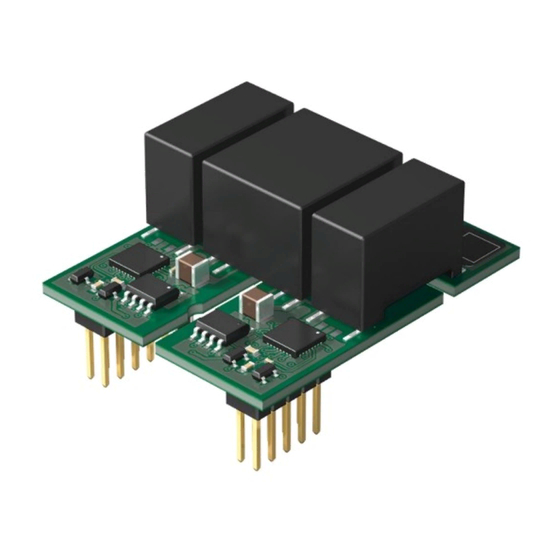
Introduction The SKYPER ® 12 PV is the most compact driver core within the SKYPER ® family and demonstrates its real advantages in low and medium power photovoltaic and ESS applications. In spite of its unrivalled compactness of only 36mm x 45mm the SKYPER ®... -
Page 3: Block Diagram And Application Example
Block Diagram and Application Example Block diagram Figure 2: SKYPER ® 12 PV | Block diagram © by SEMIKRON / 2020-05-25 / Technical Explanation / SKYPER ® 12 PV Page 3/37 PROMGT.1026/ Rev.7/ Template Technical Explanation... -
Page 4: Application Example
Optional pull-up resistor, mandatory if error output is used. 4.75kΩ nERR_OUT Dimensioning according to chapter 4.6 © by SEMIKRON / 2020-05-25 / Technical Explanation / SKYPER ® 12 PV Page 4/37 PROMGT.1026/ Rev.7/ Template Technical Explanation... -
Page 5: Secondary Side
CFG_VCE_TOP X100:01 CLMP_IN_TOP X100:07 PWR_GND_TOP X100:08 PWR_VS_N_TOP X100:10 PWR_VS_P_BOT X200:03 nERR_IN_BOT X200:04 CFG_VCE_BOT X200:01 CLMP_IN_BOT X200:07 PWR_GND_BOT X200:08 PWR_VS_N_BOT X200:10 © by SEMIKRON / 2020-05-25 / Technical Explanation / SKYPER ® 12 PV Page 5/37 PROMGT.1026/ Rev.7/ Template Technical Explanation... - Page 6 Dimensioning according to G(softoff)_BOT chapter 4.10. Optional series resistor for V -monitoring, mandatory if 511Ω VCE_TOP VCE_BOT DSCP is used. © by SEMIKRON / 2020-05-25 / Technical Explanation / SKYPER ® 12 PV Page 6/37 PROMGT.1026/ Rev.7/ Template Technical Explanation...
- Page 7 Selected by connecting pin CFG_FLT to suppression (SPS) pin PWR_GND. Undervoltage lockout Always active on primary (UVLO) and secondary side © by SEMIKRON / 2020-05-25 / Technical Explanation / SKYPER ® 12 PV Page 7/37 PROMGT.1026/ Rev.7/ Template Technical Explanation...
-
Page 8: Dimensions And Mechanical Precautions
The primary side and the two secondary side plug-in connectors are 10 pin dual row 2.54mm pin headers. For a secure mechanical connection of the SKYPER 12 PV IGBT driver it is essential that the pin headers can be fully supported by the female mating connectors. -
Page 9: Support Post
Support post To increase the robustness of the mechanical connection between the SKYPER ® 12 PV driver and the corresponding board a support post could be assembled. If a support post is used, make sure it has the correct length. A too short support post would bend both, the driver and the corresponding board that it is mounted on, thus increasing mechanical stress. -
Page 10: Handling Instructions
When handling the driver, do not pick up the driver at the transformers. The driver MUST be handled at the PCB sides. Figure 7: SKYPER ® 12 PV | Handling instruction © by SEMIKRON / 2020-05-25 / Technical Explanation / SKYPER ® 12 PV Page 10/37 PROMGT.1026/ Rev.7/ Template Technical Explanation... -
Page 11: Interface Description
X10:08 BOT_IN Switching signal input (BOT) 15V logic; 33kΩ/0.01nF (pull-down) LOW = BOT switch off HIGH = BOT switch on © by SEMIKRON / 2020-05-25 / Technical Explanation / SKYPER ® 12 PV Page 11/37 PROMGT.1026/ Rev.7/ Template Technical Explanation... -
Page 12: Pin Assignment Of Pin Header X100 | Secondary Side | Top
HIGH = No external error X200:05 BOT_ON On signal terminal for BOT External gate resistor needed semiconductor (limits under consideration of I out(avg) © by SEMIKRON / 2020-05-25 / Technical Explanation / SKYPER ® 12 PV Page 12/37 PROMGT.1026/ Rev.7/ Template Technical Explanation... -
Page 13: Power Supply | Primary Side
12 PV | Primary side | Power supply ® SKYPER 12 PV PWR_VS X10:09 PWR_VS X10:10 PWR_VS PWR_GND X10:01 PWR_GND © by SEMIKRON / 2020-05-25 / Technical Explanation / SKYPER ® 12 PV Page 13/37 PROMGT.1026/ Rev.7/ Template Technical Explanation... -
Page 14: Gate Drive Signals | Primary Side
The recommended value of the pull-down resistors is approximately 10kΩ. Parameter Threshold high Threshold low © by SEMIKRON / 2020-05-25 / Technical Explanation / SKYPER ® 12 PV Page 14/37 PROMGT.1026/ Rev.7/ Template Technical Explanation... -
Page 15: Filter Selection, Jitter And Propagation Delay Time | Primary Side
12 PV is directly connected to a nERR_OUT terminal of ® another SKYPER ® 12 PV driver, only one pull-up resistor must to be applied. © by SEMIKRON / 2020-05-25 / Technical Explanation / SKYPER ® 12 PV Page 15/37 PROMGT.1026/ Rev.7/ Template Technical Explanation... -
Page 16: Error Input | Primary Side
12 PV | 2 X10:04 nERR_IN X10:03 nERR_OUT X10:05 CFG_ERR PWR_GND X10:01 PWR_GND Parameter Threshold high 11 V Threshold low 7.5 V © by SEMIKRON / 2020-05-25 / Technical Explanation / SKYPER ® 12 PV Page 16/37 PROMGT.1026/ Rev.7/ Template Technical Explanation... -
Page 17: Error Mode Selection | Primary Side
Error mode selection | Primary side The configuration pin CFG_ERR selects the behavior of the SKYPER ® 12 PV driver core on error events. Connecting the CFG_ERR pin to the PWR_GND pin forces the driver to set its outputs to off-state immediately when an error is detected. - Page 18 CFG(temp) thermistor and the desired trip level. Parameter Threshold high 13 V Threshold low © by SEMIKRON / 2020-05-25 / Technical Explanation / SKYPER ® 12 PV Page 18/37 PROMGT.1026/ Rev.7/ Template Technical Explanation...
-
Page 19: 4.10 Gate Resistors | Secondary Side
G(softo ff)_TOP E_TOP PWR_GND_TOP X100:08 Please note that some of SEMIKRON’s driver cores using an ASIC internal N-channel MOSFET for Soft Off. To protect this MOSFET against stress when turning-off the TOP_ON/BOT_ON channel it is recommended to place the R resistor in series with the R resistor. -
Page 20: 4.11 External Boost Capacitors | Secondary Side
Please note, when assembling boost capacitors at the secondary sides, also boost capacitors have to be assembled at the primary side, as shown in Figure 9. �� = �� = �� ������ ������(��) ������(��) © by SEMIKRON / 2020-05-25 / Technical Explanation / SKYPER ® 12 PV Page 20/37 PROMGT.1026/ Rev.7/ Template Technical Explanation... -
Page 21: Protection Features
Locked immediately OFF & locked until reset OFF and locked, immediately immediately, until reset © by SEMIKRON / 2020-05-25 / Technical Explanation / SKYPER ® 12 PV Page 21/37 PROMGT.1026/ Rev.7/ Template Technical Explanation... - Page 22 This behavior prevents deadlock situations, if several drivers are using the bi-directional HALT feature, as described in chapter 4.7. © by SEMIKRON / 2020-05-25 / Technical Explanation / SKYPER ® 12 PV Page 22/37 PROMGT.1026/ Rev.7/ Template Technical Explanation...
- Page 23 1) The signal characteristics of BOT_ON/OFF and TOP_ON/OFF are valid if the outputs X100:06 and X100:07 respectively the outputs X200:06 and X200:07 are connected to each other through the gate resistors. © by SEMIKRON / 2020-05-25 / Technical Explanation / SKYPER ® 12 PV Page 23/37 PROMGT.1026/ Rev.7/ Template Technical Explanation...
-
Page 24: Dead Time And Interlock
No dead time Important Note When the interlock function is disabled a bridge shoot through has to be prevented by the user’s control unit. © by SEMIKRON / 2020-05-25 / Technical Explanation / SKYPER ® 12 PV Page 24/37 PROMGT.1026/ Rev.7/ Template Technical Explanation... -
Page 25: Short Pulse Suppression (Sps)
Secondary side non-error threshold, positive gate voltage 13.3V Secondary side shutdown threshold, negative gate voltage -4.1V Secondary side non-error threshold, negative gate voltage -5.8V © by SEMIKRON / 2020-05-25 / Technical Explanation / SKYPER ® 12 PV Page 25/37 PROMGT.1026/ Rev.7/ Template Technical Explanation... -
Page 26: Dynamic Short Circuit Protection By
SEMIKRON recommends to set the DSCP trip level to a value of 7V to 9V (voltage at the CFG_VCE pin) to prevent from unwanted accidently (false) triggered desaturation events due to a too small gap between the saturation voltage of the IGBT and the trigger level of the DSCP feature. -
Page 27: Dscp | Functional Description
V has already fallen below 10V before the monitored voltage V is below that CE(ref) CE(IN) level. © by SEMIKRON / 2020-05-25 / Technical Explanation / SKYPER ® 12 PV Page 27/37 PROMGT.1026/ Rev.7/ Template Technical Explanation... -
Page 28: Dscp | Calculation Hints
) ⋅ �� + ( �� ) ⋅ �� �� ⋅ �� + �� �� ⋅ �� + �� ������ ������ © by SEMIKRON / 2020-05-25 / Technical Explanation / SKYPER ® 12 PV Page 28/37 PROMGT.1026/ Rev.7/ Template Technical Explanation... -
Page 29: Active Clamping
12 PV | Application example for active clamping ® SKYPER 12 PV CLMP_TOP CLMP_IN_TOP X100:07 G(off)_TOP TOP_OFF X100:06 PWR_GND_TOP X100:08 & TOP_IN PWR_VS_N_TOP X100:10 © by SEMIKRON / 2020-05-25 / Technical Explanation / SKYPER ® 12 PV Page 29/37 PROMGT.1026/ Rev.7/ Template Technical Explanation... -
Page 30: Soft Off
IGBT and on the other hand reducing the overvoltage below the maximum collector-emitter voltage of the IGBT. Please observe the individual SCSOA of your power semiconductor. © by SEMIKRON / 2020-05-25 / Technical Explanation / SKYPER ® 12 PV Page 30/37 PROMGT.1026/ Rev.7/ Template Technical Explanation... -
Page 31: Safe Short Circuit Turn-Off In Multilevel Topology
SKYPER ® 12 PV allows proper control of the power semiconductors in multilevel applications. And thanks to the advanced error management provisions realized in the ASIC chipset the SKYPER ® 12 PV safely handles even short circuit conditions. -
Page 32: Product Qualification
±x, ± y, ± z The test conditions are not the maximum applicable conditions for the products. The characteristics of the products are indicated in the data sheet © by SEMIKRON / 2020-05-25 / Technical Explanation / SKYPER ® 12 PV Page 32/37 PROMGT.1026/ Rev.7/ Template Technical Explanation... -
Page 33: Environmental Conditions
-40... +85 °C High humidity 85 °C, 85% Flammability Heavy flammable materials only UL94 V0 RoHS / WEEE / China RoHS © by SEMIKRON / 2020-05-25 / Technical Explanation / SKYPER ® 12 PV Page 33/37 PROMGT.1026/ Rev.7/ Template Technical Explanation... - Page 34 IEC 60068-2-27 1000 shocks per axis), 30g, 18ms (The connection between driver and PCB was reinforced by a support post during the test.) © by SEMIKRON / 2020-05-25 / Technical Explanation / SKYPER ® 12 PV Page 34/37 PROMGT.1026/ Rev.7/ Template Technical Explanation...
-
Page 35: Marking
Figure 23: SKYPER ® 12 PV | Label Every driver core is marked with a data matrix label. The marking contains the following items. © by SEMIKRON / 2020-05-25 / Technical Explanation / SKYPER ® 12 PV Page 35/37 PROMGT.1026/ Rev.7/ Template Technical Explanation... - Page 36 [3] P. Bhosale, M. Hermwille, AN-7002 “Connection of Gate Drivers to IGBT and Controller” [4] M. Hermwille, AN-7003 “Gate Resistor – Principles and Applications” [5] J. Lamp, AN 19-001 “Gate Driver Configuration and Short Circuit Protection for 3-Level Topologies” © by SEMIKRON / 2020-05-25 / Technical Explanation / SKYPER ® 12 PV Page 36/37 PROMGT.1026/ Rev.7/ Template Technical Explanation...
- Page 37 SEMIKRON does not assume any liability arising out of the applications or use of any product; neither does it convey any license under its patent rights, copyrights, trade secrets or other intellectual property rights, nor the rights of others.
Need help?
Do you have a question about the SKYPER and is the answer not in the manual?
Questions and answers