
Summary of Contents for ABACO VMIVME-1184 Series
- Page 1 (217) 352-9330 | Click HERE Find the Abaco Systems / VMIC VMIVME-1184-000000 at our website:...
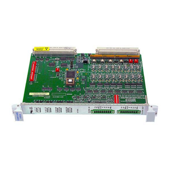
- Page 2 Hardware Reference Manual VMIVME-1184* 32-bit Optically Isolated Change-of-State (COS) Input Board with Sequence-of-Events (SOE) Publication No. 500-001184-000 Rev. B.0 Artisan Technology Group - Quality Instrumentation ... Guaranteed | (888) 88-SOURCE | www.artisantg.com...
- Page 3 WEEE is processed in accordance with the requirements of the WEEE Directive. Abaco Systems will evaluate requests to take back products purchased by our customers before August 13, 2005 on a case-by-case basis. A WEEE management fee may apply.
- Page 4 About This Manual Conventions Notices This manual may use the following types of notice: WARNING Warnings alert you to the risk of severe personal injury. CAUTION Cautions alert you to system danger or loss of data. NOTE Notes call attention to important features or instructions. Tips give guidance on procedures that may be tackled in a number of ways.
- Page 5 Abaco Website You can find information regarding Abaco products on the following website: LINK www.abaco.com Abaco Documents This document is distributed via the Abaco website. You may register for access to manuals via the website. LINK www.abaco.com/products/ Third-party Documents For a detailed explanation of the VMEbus and its characteristics, refer to ʺThe VMEbus Specificationʺ...
- Page 6 You can find technical assistance contact details on the website Embedded Support page. LINK www.abaco.com/embedded-support Abaco will log your query in the Technical Support database and allocate it a unique Case number for use in any future correspondence. Alternatively, you may also contact Abaco’s Technical Support via: LINK support@abaco.com...
- Page 7 • Data can be read using 8-, 16-, or 32-bit data transfers • Each channel can be independently set by the user to perform the following functions: – Per channel COS event storage configuration – Ignore all changes (no events stored due to this channel changing) –...
- Page 8 Because of the danger of introducing additional hazards, do not install substitute parts or perform any unauthorized modification to the product. Return the product to Abaco for service and repair to ensure that safety features are maintained. Publication No. 500-001184-000 Rev. B.0 About This Manual 7 Artisan Technology Group - Quality Instrumentation ...
-
Page 9: Table Of Contents
Table of Contents 1 • Theory of Operation ............12 1.1 Introduction. - Page 10 3.7.7 FIFO Count Register (FIFO_CNT) ..............37 3.7.8 Counter FIFO Count Register (CTR_FIFO_CNT) .
- Page 11 List of Figures Figure 1-1 VMIVME-1184 Block Diagram ............13 Figure 1-2 AM2 Line (Switch S29) .
- Page 12 List of Tables Table 1-1 COS Logic ................16 Table 1-2 Walking Ones Test .
-
Page 13: Theory Of Operation
1 • Theory of Operation 1.1 Introduction The board functions are broken down into six major blocks. These blocks are: • Bus interface • Register decoder • Interrupt Processor (IP) • Change-of-State (COS) logic • Input circuits • Counter The bus interface contains the VMEbus interface logic, the boardʹs address decoding logic and the data steering logic. -
Page 14: Vmebus Interface
Figure 1-1 VMIVME-1184 Block Diagram FPGA Broken Quadrature Wire 32-Bit Counter Detection Counter Recovery Front Panel 3 Differential Pairs Board Address RS-422 Selection Xcvr 3 Differential Pairs Interrupt Debounce Processor (IP) FIFOs Clock (+) side used for Single-Ended Address Send/Receive Decode Detection Control... -
Page 15: Data Transfer Cycles
1.2.1 Data Transfer Cycles The Address switch (S12-1) establishes the upper address line decoding. If the switch is On, the board will respond to standard accesses. If the switch is Off, the board will respond to short accesses. The default configuration is standard accesses. -
Page 16: Register Decoder
interrupts are enabled, a full FIFO will generate an interrupt with the same level and vector as COS. NOTE If COS events come faster than the CPU can service, interrupt starvation will occur, keeping regular programs from executing. Please keep this in mind when configuring your system. Be especially mindful of completely emptying the FIFO(s) and limiting the capture of events to those which are actually necessary for operation. -
Page 17: Change-Of-State Logic
1.5 Change-of-State Logic The COS logic bases its actions on the state of its select lines A and B. These lines are controlled by the COS register values. The states are listed in Table 1-1 below: Table 1-1 COS Logic SEL B SEL A COS Logic’s Action... - Page 18 During this test, two channels are actually changing value after State 1. In State 2, channel 0 has changed from a 1 to a 0, and channel 1 has changed from a 0 to a 1. Theoretically, these changes are simultaneous, and are viewed as a single COS event.
-
Page 19: Inputs
Channel 5 Channel 4 Previous State 2 COS State 2 The recovered COS FIFO data appears to have logically “anded”the previous state, and the current state of COS State 1 and Previous State 2, while the correct COS data does not appear until COS State 2. When viewed on a logic analyzer, the incoming data skew may be as little as 3 or 4 nsec, but due to synchronizing clock skew and the debounce skew, the saved COS sequence appears as two separate events. -
Page 20: Contact Closure
1.6.2 Contact Closure If the Contact Closure configuration is chosen, the user will need to insert a SIP resistor (provided) and set the appropriate pull-up voltage using either 5V, 12V or an external user-supplied voltage through contacts on channels 31 or 32. NOTE It is recommended that user supplied voltage not exceed 28V. -
Page 21: Figure 1-4 Channel 31 Input Circuitry (Channel 32 Uses Vext #2)
Figure 1-4 Channel 31 Input Circuitry (Channel 32 uses Vext #2) #1 Ext Vbank For Contact Vext Sensing Only x8 SIP (socketed) (P2-A31) High Channel 31 Detection (Switch selectable) opto-isolator (P2-C31) Low Over Voltage Chassis Protection 20 VMIVME-1184* 32-bit Optically Isolated Change-of-State (COS) Input Board Publication No. -
Page 22: Configuration And Installation
CAUTION Some of the components assembled on Abaco Systems products may be sensitive to electrostatic discharge and damage may occur on boards that are subjected to a high-energy electrostatic field. When the board is placed on a bench for configuring, etc., it is suggested that conductive material should be placed under the board to provide a conductive shunt. -
Page 23: Operational Configuration
2.4 Operational Configuration The VMIVME-1184 Boardʹs base address and I/O access mode are determined by user configurable switches. This section describes the use of these switches. The locations of the switches and jumpers on the VMIVME-1184 are shown in Figure 2-1, Switch and Jumper Locations on page 23. -
Page 24: Figure 2-1 Switch And Jumper Locations
Figure 2-1 Switch and Jumper Locations * Denotes Default Setting ALL> NonPrilileged> Supervisory> FAIL Voltage Source Selection 28V / 12V / 5V 28V / 12V / 5V CH3-4 CH1-2 CH7-8 CH5-6 CH9-10 CH10-11 CH15-16 CH13-14 CH19-20 CH17-18 CH21-22 CH23-24 CH27-28 CH25-26 CH29-30 CH31-32... -
Page 25: Debounce Timing
Table 2-1 Voltage Thresholds Voltage 25 C Exp Act 40 C Exp Act 80 C Exp Act 5V LO -> HI 1.2 1.3 1.3 1.4 1.6 1.9 12V LO -> HI 1.7 1.9 1.9 2.1 3.2 3.6 28V LO -> HI 2.5 2.9 3.1 3.6 6.1 7.3... -
Page 26: Connector Description
26 for connector pinouts. 2.6.1 Barrier Terminal Transition Panels The VMIVME-1184 can be used with Abaco’s BT0X family of BT transitions panels. The VMIACC-BT01, 02, 03 and 04 family of BT transition panels meets ANSI/IEEE SWC TEST. The BT transition panels provides a passive breakout of the discrete wires of the ribbon cables, allowing for a more efficient interface between external user equipment and Abaco’s VMEbus-based interface boards. -
Page 27: Figure 2-2 P1/P2 Connector Pin Layout
Figure 2-2 P1/P2 Connector Pin Layout PIN 1 PIN 2 REAR VIEW PIN 3 OF BOARD PIN 4 PIN 5 PIN 6 PIN 7 PIN 8 PIN 9 PIN 10 PIN 11 PIN 12 PIN 13 PIN 14 PIN 15 PIN 16 PIN 17 PIN 18... -
Page 28: Table 2-4 P2 Pin Assignments
Table 2-3 P1 Pin Assignments (Continued) Function Function Function VME_D(14) Tied to B6 VME_D(6) VME_D(15) Tied to B9 VME_D(7) Tied to B8 C10 N/C B10 Tied to B11 A10 VME_SYSCLK C11 N/C B11 Tied to B10 A11 GND C12 VME_SYSRSTn B12 N/C A12 VME_DS1n C13 VME_LWORDn... - Page 29 Table 2-4 P2 Pin Assignments (Continued) Function Function Function C17 CH(17) INPUT- B17 VME_D(19) A17 CH(17) INPUT+ C18 CH(18) INPUT- B18 VME_D(20) A18 CH(18) INPUT+ C19 CH(19) INPUT- B19 VME_D(21) A19 CH(19) INPUT+ C20 CH(20) INPUT- B20 VME_D(22) A20 CH(20) INPUT+ C21 CH(21) INPUT- B21 VME_D(23) A21 CH(21) INPUT+...
-
Page 30: Programming
3 • Programming 3.1 Introduction Throughout this manual the 32 input channels have been listed as 1-32. In this section the inputs are discussed on a logic level, and as such, will be referenced as 00-31. The VMIVME-1184 can reside in short 16-bit I/O space or standard 24-bit data space. -
Page 31: Board Id (Bd Id) Register
Table 3-1 VMIVME-1184 Address Map (Continued) Relative Address Register Name Register Function R/RW CH_INT_ENA Channel Interrupt Enable register DB_Data Debounced Data Register FREV Firmware Revision ID CSR2 Control and Status Register #2 3.1.1 Board ID (BD ID) Register Table 3-2 Board ID Register Bit Map BD ID: Offset $XXXX (fixed @ $6700) Bit 31... -
Page 32: Csr2 Bit Definitions
Bit 08: Extend Debounce - A one (1) sets the Debounce to the time indicated by bits 6 and 7. The original value is latched from onboard jumpers, but this condition can be changed through the software. Clearing this bit reduces debounce to 1µs. -
Page 33: Counter Connectivity
3.2.3 Counter Connectivity Bits 31-19 and Bit 15: Unused (reserved for future use). 3.2.4 Quadrature Counter Decoder Bits (Bits 16, 17 and 18) Bits 18 and 17 = Set debounce times 0 0 = 62.5nS 0 1 = 125nS 1 0 = 1uS 1 1 = 10uS Bit 16: 1 = Disable AB debounce (note: Marker is always debounced per... -
Page 34: Encoder Markers
3.2.5 Encoder Markers The following bits are used to control or show the status of markers in the system. Bit 07: Marker Interrupt Generation - R/W, 0 = Rising Edge only (default) 1 = Both edges NOTE If Bits 04 or 05 of CSR2 are set, then the qualified marker edges are used to generate the interrupt. Bit 06: Clear Counter (level/edge) - R/W, 0 = Counter cleared by marker level. -
Page 35: Data Fifo Register
3.3 Data FIFO Register The Data FIFO register is a read-only register, containing the stored COS or SOE data. In the SOE mode of operation, the first read of this register will yield the value of the channel inputs previous to the change-of-state that triggered the storage of data. -
Page 36: Interrupt Levels
3.4.1 Interrupt Levels These three bits (L2 through L0) set the interrupt level that the IP will present to the host when a COS, or Marker request is made. The interrupt levels and the field values are: Bits 7 through 4: Marker Interrupt Enable and Level bits. Bits 3 through 0: COS Interrupt Enable and Level bits. -
Page 37: Counter Register (Offset: $Xxxx14)
• Counter_Value • PREV_Input_Data • COS_Input_Data Figure 3-1 COS and SOE Registers Read COS Counter Data Counter Data Read 1C 0x10 0x08 0x10 0x08 Read 1F Ö Ö Read SOE Read 1C Read 1P Read 1F C = Counter F = Flagged P = Previous 3.7.1 Counter Register (Offset: $XXXX14) This register contains the current count derived from the front panel input (P3). -
Page 38: Cos Select Register 0
3.7.3 COS Select Register 0 This register’s bits are used to select the COS trigger condition for bits 31 through Table 3-10 COS Select Register 0 Bit Map COS Select Register 0 $XXXX18 Bit 31 Bit 30 Bit 29 Bit 28 Bit 27 Bit 26 Bit 25... -
Page 39: Counter Fifo Count Register (Ctr_Fifo_Cnt)
Table 3-14 FIFO Count Register Bit Map FIFO_CNT: Offset $XXXX20 Bit 15 Bit 14 Bit 13 Bit 12 Bit 11 Bit 10 Bit 09 Bit 08 Bit 07 Bit 06 Bit 05 Bit 04 Bit 03 Bit 02 Bit 01 Bit 00 3.7.8 Counter FIFO Count Register (CTR_FIFO_CNT) This 16-bit register contains the count of the number of samples in the quadrature... -
Page 40: Counter Feature
3.10 Counter Feature The VMIVME-1184 has the capability of accepting a counter input (either single- ended or differential) at the P3 connector on the front panel. A single channel (A) can be used for incremental counting. Two channels are required to function as full Quadrature. -
Page 41: Quadrature Mode
Figure 3-2 Leading Edge Example “A leading B” example “B leading A” example Figure 3-3 1x Counter Mode All rising edges of “A” increment counter B Ignored in this mode Figure 3-4 2x Counter Mode Any edges of “A” increment counter B Ignored in this mode 3.11.2 2X Quadrature Mode If input A leads input B, the module counts up on both rising and falling edges of... -
Page 42: Quadrature Mode
3.11.3 4X Quadrature Mode If input A leads input B, the module counts up on both rising and falling edges of inputs A and B. If input B leads input A, the module counts down on the rising and falling edges of inputs A and B. This mode is set through CSR1 Bits 5 and 4. CRS1_[5] = 1 CSR1_[4] = 1 Figure 3-6... -
Page 43: Vmivme-1184 Inputs
The board will operate in SOE mode, with a counter (using the Marker to reset the counter) input through the front panel connector P3. To program the interrupts, assign an interrupt level and vector for the COS and Marker. We will assign interrupt level 4 to COS/SOE interrupts, and a interrupt vector value of $83. -
Page 44: Marker Gating
3.14 Marker Gating Figure 3-7 Marker Gating Diagram Inputs Bits Results 5 4 3 2 1 Matches “M” input 0 0 X X 1 1 0 1 X 1 “M” gated with “A” 1 1 1 1 1 “M” gated with both “A” and “B” 0 0 X X 0 Exact inverse of “M”... - Page 45 © 2016 Abaco Systems, Inc. All rights reserved. Information Centers For more information, please visit the * indicates a trademark of Abaco Systems, Inc. and/or its affiliates. All other Abaco Systems website at: Americas: trademarks are the property of their 1-866-652-2226 (866-OK-ABACO) respective owners.
Need help?
Do you have a question about the VMIVME-1184 Series and is the answer not in the manual?
Questions and answers