Philips DCD322/12 Service Manual
Hide thumbs
Also See for DCD322/12:
- User manual (31 pages) ,
- Quick start manual (2 pages) ,
- Specification sheet (3 pages)
Table of Contents
Advertisement
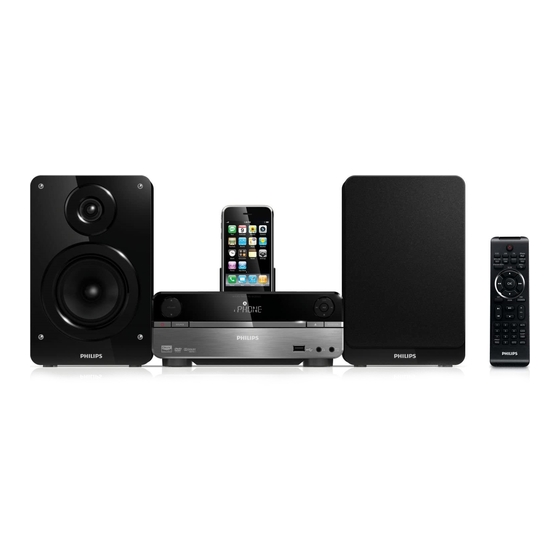
DVD Micro System
Contents
2 Laser Beam Safety Precautions.................................2-1
3 Important Safety Precautions ..........................3-1 to 3-2
4 Safety Check After Servicing .................................... 4-1
Requirements ............................................................5-1
7 Direction of Use ...............................................7-1 to 7-5
8 Cabinet Disassembly Instructions ................... 8-1 to 8-2
9 Troubleshooting .............................................. 9-1 to 9-2
10 Block Diagram ........................................................10-1
11 Wiring Diagram ...................................................... 11-1
12 AMP Board
Circuit Diagram .................................12-1
Layout Diagram ................................12-2
13 Display Board
Circuit Diagram .................................12-3
Layout Diagram ................................12-4
© Copyright 2010 Philips Consumer Electronics B.V. Eindhoven, The Netherlands.
All rights reserved. No part of this publication may be reproduced, stored in a
retrieval system or transmitted, in any form or by any means, electronic,
mechanical, photocopying, or otherwise without the prior permission of Philips.
Published by LX-KM 1036 AVM
Version 1.1
Recordable
Page
Printed in the Netherlands
ReW ritabl e
Contents
14 Headphone and USB Board
Circuit Diagram .................................12-5
Layout Diagram ................................12-5
15 Power Board
Circuit Diagram ...............................12-6 to 12-7
Layout Diagram ...............................12-8
16 IPOD Board
Circuit Diagram ..............................12-9
Layout Diagram .............................12-9
Circuit Diagram ..............................12-10 to 12-13
Layout Diagram .............................12-14
18 Exploded View......................................................13-1
19 Revision List .........................................................14-1
Subject to modi cation
DCD322/12
Page
3141 785 35501
EN
Advertisement
Table of Contents

Related Manuals for Philips DCD322/12


Summary of Contents for Philips DCD322/12
-
Page 1: Table Of Contents
Circuit Diagram .........12-3 Layout Diagram ........12-4 © Copyright 2010 Philips Consumer Electronics B.V. Eindhoven, The Netherlands. All rights reserved. No part of this publication may be reproduced, stored in a retrieval system or transmitted, in any form or by any means, electronic, mechanical, photocopying, or otherwise without the prior permission of Philips. -
Page 2: Technical Specification And Connection Facilities And Version Variation
Technical Specification and Connection Facilities 1. Technical Specification and Connection Facilities 1.1 PCB Locations Headphone and USB Board Display Board DVD Loader Power Board AMP Board Decoder Board CVBS 1.2 General Amplitude Output : 1Vpp±10% White Bar : 714mV±10% Sync.Amplitude : 286mV±10% Power supply : 100-240V, 50Hz~60Hz... - Page 3 Technical Specifications and Connection Facilities 1.5 Dimension and Weight Main Unit (WxHxD) : 223X88X242mm Net Weight : 1.8kg Speaker Box (WxHxD) : 140x220x220mm Net Weight : 3.9kg 1.6 Playability Video Playback 1. Playback Media: CD-R/CD-RW, DVD+R/+RW, DVD-R/-RW, DVD-Video, Video CD/SVCD, DVD+R DL, DVD-R DL,USB flash drive 2.
-
Page 4: Laser Beam Safety Precautions
Laser Beam Safety Precautions This Blu-Ray player uses a pickup that emits a laser beam. Do not look directly at the laser beam coming from the pickup or allow it to strike against your skin. The laser beam is emitted from the location shown in the figure. When checking the laser diode, be sure to keep your eyes at least 30 cm away from the pickup lens when the diode is turned on. -
Page 5: Important Safety Precautions
Remove discs from the disc compartment and the wall mount. Koninklijke Philips if you are not using the product for an Electronics N.V. bears no responsibility extended period of time. - Page 6 Important Safety Precautions Disposal of your old product and batteries Your product is designed and manufactured with high quality materials and components, which can be recycled and reused. When this crossed-out wheeled bin symbol is attached to a product it means that the product is covered by the European Directive 2002/96/EC.
-
Page 7: Safety Check After Servicing
Safety Check after Servicing Examine the area surrounding the repaired location for damage or deterioration. Observe that screws, parts, and wires have been returned to their original positions. Afterwards, do the following tests and confirm the specified values to verify compliance with safety standards. 1. -
Page 8: Safety Information General Notes & Lead Free Requirements
Safety Information, General Notes & Lead Free Requirements Safety Instructions Warnings General Safety General Safety regulations require that during a repair: All ICs and many other semiconductors are susceptible to Connect the unit to the mains via an isolation transformer. electrostatic discharges (ESD, ). -
Page 9: Standard Notes For Servicing,Lead Free Requirements & Handling Flat Pack Ic
When soldering, be sure to use the Pb free solder. indicated as shown. Information about lead-free soldering Top View Bottom View Philips CE is producing lead-free sets from 1.1.2005 onwards. Input IDENTIFICATION Regardless of special logo (not always 2. For other ICs, pin 1 and every fifth pin are indicated) indicated as shown. - Page 10 2004), containing leaded solder-alloy and components, all needed spare-parts will be available till the end of the service-period. For repair of such sets nothing changes. On our website www.atyourservice.ce.Philips.com you find more Fig. S-1-1 information to: BGA-de-/soldering (+ baking instructions) 2.
- Page 11 Standard Notes for Servicing, Lead Free Requirements & Handling Flat Pack IC 3. The flat pack-IC on the CBA is affixed with glue, so 4. Release the flat pack-IC from the CBA using be careful not to break or damage the foil of each tweezers.
- Page 12 Standard Notes for Servicing, Lead Free Requirements & Handling Flat Pack IC 2. Installation Instructions for Handling Semi- 1. Using desoldering braid, remove the solder from conductors the foil of each pin of the flat pack-IC on the CBA Electrostatic breakdown of the semi-conductors may so you can install a replacement flat pack-IC more occur due to a potential difference caused by easily.
-
Page 13: Direction Of Use
The following excerpt of the DFU/QSG serves as an introduction to the set. The Complete Direction for Use can be download in different languages from the internet site of Philips Customer care Center : www.support.philips.com Remote control Overview of the main unit... - Page 14 Direction of Use Remote control ANGLE/PROG AUDIO Select a DVD camera angle. For VCD, select stereo, mono-left or mono-right channel. Program tracks. For DVD/DivX video, select an audio Program titles/chapters for DVD play. language. Program radio stations. Numeric keypad Search in a track or disc. Select a title/chapter/track directly.
- Page 15 Direction of Use Connect the supplied FM wire antenna to Note the FM AERIAL socket on the unit. To avoid magnetic interference or unwanted noise, never place this apparatus and speakers too close to any radiation devices. Place this unit on top of a table or mount it on the wall.
- Page 16 Direction of Use Connect an S-video cable (not supplied) Option 2: Connect through analog audio cables the S-Videosocket on this unit. the S-Videosocket on the TV. Option 2: Connect through a composite video cable L LINE IN R Connect an audio cable (red/white ends) the AUDIO OUT (L andR) sockets on this unit.
- Page 17 Direction of Use Connect component video cables (red/ blue/green - not supplied) to: the COMPONENT (Pr/Cr Pb/Cb Y) sockets on this unit. the component input sockets on the TV. AUDIO OUT Option 4: Connect through the iPhone/iPod socket You can view video es that are stored on your iPhone/iPod on your TV.
-
Page 18: Decoder Board
Cabinet Disassembly Instructions 1. Disassembly Flowchart Note: (1) Identification (location) No. of parts in the figures This flowchart indicates the disassembly steps to gain (2) Name of the part access to item(s) to be serviced. When reassembling, (3) Figure Number for reference follow the steps in reverse order. - Page 19 Cabinet Disassembly Instructions Fig.D3 Fig.D6 Fig.D4 Fig.D5...
-
Page 20: Troubleshooting
Troubleshooting FLOW CHART NO.1 Check the Power Cord is connected Check power PCB location F1(FUSE) whether open Try to replace a new FUSE Check whether the PowerBoard has +22v&5v provided voltage output Check&replace a new power PCB FLOW CHART NO.2 Has not voice form the speaker Adjust the Volume Retry again... - Page 21 Troubleshooting FLOW CHART NO.4 Pass in and out can not read dish sometime. Check dish if put on the right position or not. Check dish if cleanlily or not. FLOW CHART NO.5 Can not pass in and out Check pin connector location CN4 at decoder board is loose or not FLOW CHART NO.6 Can not read dish Check cable locatio CN2 is loose or not...
-
Page 22: Block Diagram
Block Diagram M1.8V M3.3V M3.3V Foryou pick up SDRAM DM-06BXLX-L2 1M * 16 DVD Loader K4S161622C-TC/L70 M3.3V MAIN BOARD AMPLIFIER BOARD Loader motor driver M3.3V SERIAL FLASH CD5888 AT26DF081A M1.8V Main chipset pb/cb pr/cr Open/Close Driver ZR36966XD OPEN DOOR S-VIDEO COAXIAL PHONE L&R Door Detect... -
Page 23: Wiring Diagram
Wiring Diagram Designator2 3P/2.0 Comment MP3-L MP3-R STBY HP-L HP-R MUTE HP-MUTE L-CH R-CH IPOD-VCC IPOD-TX 5P/2.0 IPOD-TR IPOD-DET IPOD-L IPOD-L IPOD-R IPOD-R REST MCLK Headphone、USB Board Decoder Board 10P/1.25 Display Board CN101 10P/1.25 5P/2.0 6P/2.0 11-1 11-1... -
Page 24: Circuit Diagram
AMP Board -- Circuit Diagram TDA7492 SUB_GND OUTPA R26 5.6K C110 100P C115 INPA OUTPA 2.2UF R110 22UH/5A 2.2k R301 8R C114 INNA PGNDA L1 COIL4 152P C116 C118 C301 C119 SGND PGNDA 330P CN302 R116 C121 VDDS VDDS PVCCA C302 R117 5P/2.0... -
Page 25: Layout Diagram
AMP Board -- Layout Diagram 12-2 12-2... - Page 26 Display Board -- Circuit Diagram REMOTE S101 LCD101 R103 47 C104 R126 C103 47U/6.3V R110 LED102 R102 Q104 8050 2.2K R113 seg12 SEG12 seg11 SEG11 seg10 SEG10 DATA seg9 DATA SEG9 LED101 U101 seg8 R105 10k SEG8 seg7 OSCI SEG7 seg6 HT1622(44QFP) SEG6...
-
Page 27: Layout Diagram
Display Board -- Layout Diagram 12-4 12-4... -
Page 28: Layout Diagram
Headphone and USB Board -- Circuit and Layout Diagram USB Board Headphone Board JA202A JA203 R202 47K C202 100P R201 47K DGND C201 100P Shield VBUS CN203 vbus 4P/2.0 CN202 4P/2.0 USB Board Headphone Board R203 C203 12-5 12-5... -
Page 29: Circuit Diagram
Power Board -- Circuit Diagram 1 D6 D7 D8 Lp=0.56mH 471M/400V +19.5V UU15-30mH DR6*15 3uH 4A/600V UF5404 103/1KV 0.1uF/275V 82uF/400V 103/600V 102/1KV 104/50V R22 33R/2W 2*1000uF/25V 1000uF/25V 4*1M 1206 471M/400V 102/1206/500V MF72 10D9 +5.2V SB360 DR6*15 2uH 10K/1206 10K/1206 3R3/1206 IN4007 CON1 1000uF/10V... - Page 30 Power Board -- Circuit Diagram 2 102pF/500V 0.47ohm x2 CE11 CE12 CE13 CE10 CON3 SB3100 10uH/0.6mm +5.1V/1.0A 160uH/0.5mm T1-C 471pF/50V MC34063A SB240 104pF/50V 1000uF/10V 104/50V/0805 1000uF/25V 5*220uF/25V 9.1K/0805 104/50V 3K/0805 150K/0805 104/50V/1206 12-7 12-7...
- Page 31 Power Board -- Layout Diagram 12-8 12-8...
-
Page 32: Layout Diagram
IPOD Board -- Circuit and Layout Diagram IP201 30P-IP DGND LCH_IPOD R401 1K RCH_IPOD AGND LCH_IPOD AGND Right RCH_IPOD IPOD_DET Left AGND R403 1K Right In video R405 Left In R402 0 DGND SGND IPOD_DET Video Out video IPOD-AC DGND R407 100 CN401 R408 100... -
Page 33: Circuit Diagram
Decoder Board -- Circuit Diagram 1 VDDPWM VDDAFE MBW2012-221 DRVSB DRVSB OPEN-M OPEN-M OSCOUT C2 22pF CLOSE-M 10nF CLOSE-M R1 75R HOMESW HOMESW VDDAFE DSPVCC33 27.000MHz 220K MBW2012-221 OSCIN C7 22pF 10nF 100uF/10V 10nF VDDDAC DSPVCC33 DSPVCC33 FOCUS_PWM MBW2012-221 TRACK_PWM 33pF EC30 SPDL_PWM... - Page 34 Decoder Board -- Circuit Diagram 2 DSPVCC33 MD_DVD 3.3R 0.1uF [470pF] [470pF] MD_CD 220uF/6.3V SPDL_SENS- SP_M- [NM] SPDL_SENS- 220R LD_DVD BT2907 [NM] VR_CD DSPVCC33 DSPVCC33 VR_DVD 2.2R 2.2R 0.1uF 3.3R [91R] [91R] BAT54C 220uF/6.3V 24Pin OPU connector SP_MOT- SPDL_SENS+ SPDL_SENS+ 220R LD_CD BT2907...
- Page 35 Decoder Board -- Circuit Diagram 3 MUTE_CTL MUTE-AP MUTE_CTL 4.7K 75pF APWM_R- 1N4148 1N4148 L_AUX2_IN R_AUX2_IN MUTE-MCU MUTE-MCU EC15 1.2nF CF4558 1N4148 DVD_IN_R PH-3A 10u/16V AUDIO_VCC 1N4148 AP-R-OUT 0.1uF AP-L-OUT MUTE-AP MUTE-PH ECO-POWER line/phone/mute ECO-POWER 1N4148 2.0*5PIN R_IPOD_IN AUX2-IN-R 4.7K 75pF APWM_L- L_IPOD_IN...
- Page 36 Decoder Board -- Circuit Diagram 4 AV6-8.4-13B R444 S/PDIF_OUT C428 0.1uF COAX_SPDIF STBY5V S/PDIF_OUT COAX_SPDIF MCU3.3V FB405 1K R445 150R C-Pb_OUT CVBS_C CVBS_OUT CVBS_C AO3407 R430 C121 C410 0.1uF C421 NC(100pF) 22pF 150pF G-Y_OUT R120 10K C150 NC(100pF) FB406 1K R107 MCU-SCL Y_R_V...
- Page 37 Decoder Board -- Layout Diagram 12-14 12-14...
-
Page 38: Exploded View
Exploded View 13-1 13-1... -
Page 39: Revision List
Revision List Revision List Version 1.0 * Initial Release 14-1...
Need help?
Do you have a question about the DCD322/12 and is the answer not in the manual?
Questions and answers