
Subscribe to Our Youtube Channel
Related Manuals for AVT AVT-718

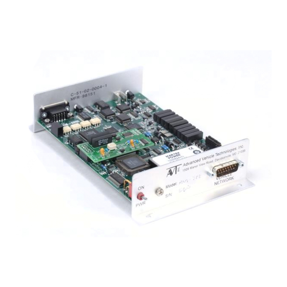
Summary of Contents for AVT AVT-718
- Page 1 (217) 352-9330 | Click HERE Find the Advanced Vehicle Technologies AVT-718 at our website:...
- Page 2 ADVANCED VEHICLE TECHNOLOGIES, Inc. AVT-718 Multiple Interface RS-232 or RS-422 Unit User’s Manual 1509 Manor View Road Davidsonville, MD 21035 410-798-4038 (voice) 410-798-4308 (fax) www.AVT-HQ.com support@AVT-HQ.com Revision ‘C1’ 19 October 2004 Artisan Technology Group - Quality Instrumentation ... Guaranteed | (888) 88-SOURCE | www.artisantg.com...
-
Page 3: Table Of Contents
3.8 CAN....................................9 3.9 J1850 VPW .................................10 3.10 J1850 PWM................................10 3.11 KWP 2000 .................................10 3.12 UBP ...................................10 3.13 LIN ....................................10 3.14 M ...............................12 ICROSECOND LOCK 4. AVT-718 OPERATION ..............................12 4.1 I ..................................12 NDICATORS 4.2 RS-232..................................12 4.3 RS-422..................................13 4.4 V ..............................13 EHICLE ETWORKS 5. - Page 4 NFORMATION 6.3.1 Fuse F1 ................................22 6.3.2 Jumper Block JP1 ..............................23 6.3.2.1 AVT-718 PC board revision levels “A” to “F” ....................... 23 6.3.2.2 AVT-718 PC board revision level “G”..........................23 6.3.2.3 AVT-718 PC board revision level “AA”......................... 24 6.3.3 Jumper JP2 ................................28 6.3.4 Connector P1 ...............................28...
-
Page 5: Introduction
1. INTRODUCTION This manual covers the AVT-718 Multiple Protocol Interface unit. It provides technical information on using the interface, connections to it, communications with it, and other related information. The AVT-718 Multiple Protocol Interface supports the following network protocols. • CAN (Controller Area Network). -
Page 6: Specifications
• Power dissipation: 3.0 watts (nominal). MTBF (Mean Time Between Failure) • MTBF information has not been discovered for many components used on the AVT-718 Multiple Interface board. The known values follow: ♦ Relays (all except K4 and K5): 500 million operations. -
Page 7: Connecting & Using
2. Connecting & Using Prior to using the AVT-718 the baud rate of the serial link between it and the host computer must be properly set. The interface must then be connected to both the subject vehicle and the host computer. -
Page 8: Connections
2.2 Connections Initial use and testing require that the AVT-718 be connected to a power supply and the host computer serial port. Refer to Sections 6.3.2, 6.3.6, and 6.3.7 for pin assignments of the AVT-718 connectors. The external power source should be a nominal +12v (minimum of +9.0v and maximum of +30.0v). -
Page 9: Interface Hardware
• At this point the AVT-718 hardware is operational. 3. Interface Hardware The following sections provide a brief description of the hardware implementation of the AVT-718. A block diagram of the AVT-718 Multiple Interface is shown in Figure 1. Included on the block diagram are all signal assignments and pin numbers for JP1 and P3. -
Page 10: Flash
FLASH device. Contact the factory if you want to update the firmware on your AVT-718 unit. We can supply, by e-mail, the firmware file and a program to update the AVT-718 FLASH device. We can provide a DOS and/or a Win95/98/NT/2000/XP program for the host computer to update the AVT-718 FLASH device. -
Page 11: J1850 Vpw
The AVT-718, in LIN mode of operations supports both Master and Slave communications on a message by message basis. Additionally, when not commanded to perform as either a Master or a Slave, the AVT-718 passively monitors the network, receives all network traffic, and forwards it all to the host. - Page 12 Power Regulation Transient Isolated Batt + & Protection DC - DC Converter Distribution Sig. Gnd. Chassis Gnd. Power L E D (green) Figure 1 AVT-718 Block Diagram Artisan Technology Group - Quality Instrumentation ... Guaranteed | (888) 88-SOURCE | www.artisantg.com...
-
Page 13: Microsecond Clock
3.14 Microsecond Clock The AVT-718 utilizes a free running 24-bit microsecond clock for all time related functions. This includes message time stamps and byte and message time intervals in KWP, UBP, and LIN modes; all of which are heavily time dependent for proper operations. -
Page 14: Rs-422
AVT-718 expects RXD to idle low and CTS to idle high. (All voltages measured with respect to the communications isolated ground.) The user should be aware of potential communications errors that may occur when using RS-232 at the higher data rates or in an electrically noisy environment. -
Page 15: Transmit Message Format
In UBP mode of operation, when a message is transmitted onto the network, the AVT-718 will issue a receive message report to the host, along with a status byte. The AVT-718 will also issue a separate transmit status report. -
Page 16: Transmit Message Status Byte Definitions
68 6A F1 01 00 The user assembles and sends the following packet to the AVT-718: 05 68 6A F1 01 00 After the AVT-718 has transmitted the message onto the network, successfully, the user receives the following at the host computer: 01 60 5.1.4 Receive message format... -
Page 17: Received Message Example
As an example the byte sequence $A7 $B6 $C5 plus CRC or checksum byte appears on the network. The message is received by the AVT-718 and the following byte sequence is passed to the host computer: $04 $00 $A7 $B6 $C5 (time stamping is disabled). -
Page 18: Alternate Header Formats
For example, the host wants to transmit the following message onto the bus: A1 B2 C3 D4 E5 F6 A7 B8 C9 DA EB FC AD BE The following messages from the host to the AVT-718 are all equivalent. The header byte(s) are bold and underlined for clarity. -
Page 19: Vpw Mode
PWM mode. 5.3.1 PWM Active Node One mode is where the AVT-718 is an active node. As such it is capable of receiving and transmitting network messages. Note that only messages destined for the AVT-718 will be received from the network, acknowledged to the network, and forwarded to the host computer. -
Page 20: Pwm "Look Alike
PWM mode includes the CRC byte at the end. If the AVT-718 is put into PWM mode and “Look Alike” is enabled the user can treat the AVT- 718 as if it were in VPW mode (for OBD-II queries). The AVT-718 will change the “68” byte from the host to “48”, the source address byte is stripped out and used to update the HBCC node... -
Page 21: Can Mode
The “Keep Alive” message can be changed or disabled by the user. 2. Issue the $61 04 command. This will shut the K-line relay and connect the AVT-718 unit to the network K-line. Unless changed by the operator (using the 53 03 xx yy command) the AVT-718 defaults to the K-line baud rate of 10.4 kbps. -
Page 22: Status And Error Codes
It is desired to receive all messages (at the host) where the third byte of the message is equal to $F1. Send the command $32 $03 $F1 to the AVT-718 interface. To verify the table entry send the command $30. The response will be $42 $03 $F1. The only network messages passed to the host will now be of the form: $zz $xx $F1 $... -
Page 23: Technical Support
Information about the enclosure is contained in Section 6.4. 6.3.1 Fuse F1 Fuse F1 on the AVT-718 board is a 500 milliamp fast blow fuse designed to protect the AVT- 718 in the event of reverse voltage application or a voltage surge significant enough to trip the input transient voltage suppressor. -
Page 24: Jumper Block Jp1
6.3.2 Jumper Block JP1 Note the different configurations, depending on PC board revision level. The AVT-718 board name, the date, and the board revision level can all be found on the bottom of the board, in copper. Note that the PC board revision level does have to match (and often will not match) the revision level noted in the white block on the top of the board. -
Page 25: Avt-718 Pc Board Revision Level "Aa
The default configuration for JP1 is the first 7 pin pairs and the last pin pair are shunted. The default configuration is shown in Table 2. Refer to the AVT-718 unit block diagram, Figure 1. Included on the block diagram are all signal assignments and pin numbers for JP1 and P3. -
Page 26: Avt-718 Block Diagram Figure 2 Diagram Of Djp1 ( Board Revisions "A" To "F")
Edge of board J P 1 Figure 2 Diagram of JP1 (board revisions “A” to “F”) AVT-718 Signal JP1 pin # JP1 pin # P3 pin # VPW bus shunt PWM bus + shunt PWM bus - shunt K-line shunt... -
Page 27: F 3 Djp1 ( "G")
Edge of board Figure 3 Diagram of JP1 (board revision “G”) AVT-718 Signal JP1 pin # JP1 pin # P3 pin # VPW bus shunt PWM bus + shunt PWM bus - shunt K-line shunt L-line shunt CAN - H... - Page 28 AVT-718 Signal JP1 pin # JP1 pin # P3 pin # VPW bus shunt PWM bus + shunt PWM bus - shunt K-line shunt L-line shunt CAN - H shunt CAN - L shunt UBP / LIN P3 pin #9...
-
Page 29: Jumper Jp2
Edge of board Figure 4 Diagram of JP2 6.3.4 Connector P1 Connector P1 exists on the AVT-718 board to support development, test, and debugging operations. It may not be installed. Do not connect anything to P1. 6.3.5 Connector P2 Connector P2 contains all unused microcontroller pins, I/O ports, TPU ports, etc. It may not be installed. -
Page 30: Connector P3
There may be signal conflicts that could result in damage to the AVT-718 and/or vehicle. It is for this reason that JP1 is available on the AVT-718 board - the user can change the signal to pin configuration on the AVT-718 to match the vehicle signal pin-out on the OBD-II connector. -
Page 31: Rs-232 Baud Rate Selection Table 5 Connector P3 ( Revisions "A" To "G")
P3 Pin # Where to Description OBD-II Connector [using AVT OBD-II cable] JP1 pin 19 JP1 pin 2 J1850 bus + JP1 pin 4 JP1 pin 18 ground plane Ground Ground ground plane Ground Ground JP1 pin 12 JP1 pin 8... -
Page 32: Connector P4
Table 6 Connector P3 (revisions “AA” and later) 6.3.7 Connector P4 Connector P4 on the AVT-718 is a DE-9S connector and will mate to any industry standard DE-9P connector. Through this connection the control computer communicates with the AVT-718 Multiple Interface. Hardware handshaking (RTS/CTS) is required for proper operation of the AVT-718. -
Page 33: Able 7 P4 Pin Escriptions , Rs-232
Pin Number Name Function / Description Direction output (through a 10K ohm pull-up resistor) Transmit Data output Receive Data input Internally connected to DSR, pin #6 Sig. Gnd. Isolated from vehicle ground Internally connected to DTR, pin #4 Clear To Send input Ready To Send output... -
Page 34: Avt-718 Enclosure
6.4 AVT-718 Enclosure The AVT-718 enclosure is easily opened to permit access to the baud rate selection shunts on JP2; the signal assignments on JP1; and fuse F1. To open the enclosure, turn it upside down. Remove the two recessed screws holding the top and bottom half together. - Page 35 Technologies can provide is available by calling, faxing, or writing. Advanced Vehicle Technologies, Inc. 1509 Manor View Road, Davidsonville, MD 21035 410-798-4038 (voice) 410-798-4308 (fax) Home Page: www.AVT-HQ.com e-mail: support@AVT-HQ.com Revision Record: Original release. Corrected an error on page 15 regarding the “A1 xx” response for a UBP transmitted message.
Need help?
Do you have a question about the AVT-718 and is the answer not in the manual?
Questions and answers