
Summary of Contents for ABACO PCIE-5565RC Series
- Page 1 (217) 352-9330 | Click HERE Find the Abaco Systems PCIE-5565RC-200000 at our website:...
- Page 2 Hardware Reference Manual PCIE-5565RC* Ultrahigh Speed Fiber-Optic Reflective Memory with Interrupts THE PCIE-5565RC IS DESIGNED TO MEET THE EUROPEAN UNION (EU) RESTRICTION OF HAZARDOUS SUBSTANCE (ROHS) DIRECTIVE (2002/95/EC) CURRENT REVISION. Publication No. 500-9300875565-000 Rev. C.0 Artisan Technology Group - Quality Instrumentation ... Guaranteed | (888) 88-SOURCE | www.artisantg.com...
- Page 3 WEEE is processed in accordance with the requirements of the WEEE Directive. Abaco Systems will evaluate requests to take back products purchased by our customers before August 13, 2005 on a case-by-case basis. A WEEE management fee may apply.
-
Page 4: About This Manual
About This Manual Conventions Notices This manual may use the following types of notice: WARNING Warnings alert you to the risk of severe personal injury. CAUTION Cautions alert you to system danger or loss of data. NOTE Notes call attention to important features or instructions. Tips give guidance on procedures that may be tackled in a number of ways. -
Page 5: Further Information
Abaco Website You can find information regarding Abaco products on the following website: LINK www.abaco.com Abaco Documents This document is distributed via the Abaco website. You may register for access to manuals via the website. LINK www.abaco.com/products/pcie-5565rc/p2239 Third-party Documents PCI Express™ Card Electromechanical Specification Revision 1.0a April 15, 2003 PCI Local Bus Specification, Rev. -
Page 6: Technical Support Contact Information
You can find technical assistance contact details on the website Embedded Support page. LINK www.abaco.com/embedded-support Abaco will log your query in the Technical Support database and allocate it a unique Case number for use in any future correspondence. Alternatively, you may also contact Abaco’s Technical Support via: LINK support@abaco.com... -
Page 7: Fcc Part 15
United States • FCC Part 15, Subpart B, Section 109, Class A • CISPR 22 (1997), Class A • ANSI C63.4 (2003) method Australia/New Zealand • AS/NZS CISPR 22 (2002) Class A using: • EN55022 (1998) Class A Japan • VCCI (April 2005) Class A using: •... -
Page 8: Safety Summary
Because of the danger of introducing additional hazards, do not install substitute parts or perform any unauthorized modification to the product. Return the product to Abaco for service and repair to ensure that safety features are maintained. Publication No. 500-9300875565-000 Rev. C.0 About This Manual 7 Artisan Technology Group - Quality Instrumentation ... -
Page 9: Overview
Overview The PCIE-5565RC* is the PCI Express (PCIe) member of Abaco’s family of Reflective Memory real-time fiber-optic network products. Two or more PCIE- 5565RCs, along with other members of this family, can be integrated into a network using standard fiber-optic cables. Each board in the network is referred to as a “node.”... -
Page 10: Vendor And Device Identification
Vendor and Device Identification The PCI Configuration register reserved for the vendor ID has the value of $114A, which designates Abaco. The PCI Configuration register reserved for the device ID has the value of $5565, which is Abaco’s board type. -
Page 11: Block Diagram
Block Diagram Figure 1 Block Diagram of PCIE-5565RC 10 PCIE-5565RC* Ultrahigh Speed Fiber-Optic Reflective Memory with Interrupts Publication No. 500-9300875565-000 Rev. C.0 Artisan Technology Group - Quality Instrumentation ... Guaranteed | (888) 88-SOURCE | www.artisantg.com... -
Page 12: Figure 2 Typical Reflective Memory Network
Figure 2 Typical Reflective Memory Network Publication No. 500-9300875565-000 Rev. C.0 About This Manual 11 Artisan Technology Group - Quality Instrumentation ... Guaranteed | (888) 88-SOURCE | www.artisantg.com... -
Page 13: Table Of Contents
Table of Contents About This Manual ........... 3 Conventions . - Page 14 3.3.7 Network Target Data Register ..............60 3.3.8 Network Target Node Register .
- Page 15 List of Figures Figure 1 Block Diagram of PCIE-5565RC ............10 Figure 2 Typical Reflective Memory Network .
- Page 16 List of Tables Table 1-1 Example Node ID Switch S2 RFM-5565 ........... . . 19 Table 1-2 Switch S1 Configuration RFM-5565 .
- Page 17 Table 3-41 PCI PIO Direct Slave Local Base Address (Remap) ......... . 50 Table 3-42 Memory Map of the Local Control and Status Registers .
-
Page 18: Handling And Installation
Abaco Systems Customer Care. 1.2 Handling Precaution Some of the components assembled on Abaco’s products may be sensitive to electrostatic discharge and damage may occur on boards that are subjected to a high-energy electrostatic field. When the board is placed on a bench for configuring, etc., it is suggested that conductive material should be placed under... -
Page 19: Switch S1 And S2 Configuration
1.3 Switch S1 and S2 Configuration Prior to installing the RFM-5565 in a host system, the desired node ID must be set using switch S2. Each node in the network must have a unique node ID. See Figure 1-1 on page 20 for the location of switch S2. Switch S2 corresponds to 8 node ID select signal lines. -
Page 20: Table 1-1 Example Node Id Switch S2 Rfm-5565
NOTE S1 position 8 should be set in the ON position only when a flash update of the control logic has failed. After a successful flash update of the control logic, S1 position 8 should be set in the OFF position. Table 1-1 Example Node ID Switch S2 RFM-5565 Node ID Position... -
Page 21: Figure 1-1 S1 And S2 Location Pcie-5565Rc
Figure 1-1 S1 and S2 Location PCIE-5565RC 20 PCIE-5565RC* Ultrahigh Speed Fiber-Optic Reflective Memory with Interrupts Publication No. 500-9300875565-000 Rev. C.0 Artisan Technology Group - Quality Instrumentation ... Guaranteed | (888) 88-SOURCE | www.artisantg.com... -
Page 22: Physical Installation
Do not install or remove the board while power is applied. Host PCI Express compatible sites vary widely in appearance and board installation procedures. Abaco recommends examining the host system installation procedures prior to installing this board. The following procedure outlines the installation of the PCIE-5565RC onto a suitable motherboard with an available PCIe connector (x4, x8, or x16). -
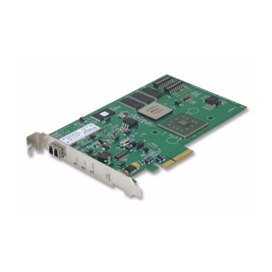
Page 23: Front Panel Description
1.5 Front Panel Description The PCIE-5565RC has an optical transceiver and three LEDs located on the front panel illustrated in the figure below. Table 1-3 on page 23 outlines the front panel’s LEDs. The port labeled “RX” is the receiver and the port labeled “TX” is the transmitter. -
Page 24: Led Description
1.5.1 LED Description Table 1-3 LED Descriptions Color Description Status User defined board status indicator. SIG. DET. Yellow Indicates optical network connection. Own Data Green Indicates when own data is received. The status LED’s power up default state is ON. The status LED is a user defined board indicator and can be toggled ON or OFF by writing to Bit 31 of the Control and Status register. -
Page 25: Figure 1-4 Lc Type Fiber-Optic Cable Connector
Figure 1-4 LC Type Fiber-Optic Cable Connector 0.84 (21.23) (4.5mm) 0.49 (1.25) Dimensions: inches (mm) 24 PCIE-5565RC* Ultrahigh Speed Fiber-Optic Reflective Memory with Interrupts Publication No. 500-9300875565-000 Rev. C.0 Artisan Technology Group - Quality Instrumentation ... Guaranteed | (888) 88-SOURCE | www.artisantg.com... -
Page 26: Figure 1-5 Example: Six Node Ring Connectivity Pcie-5565Rc
Figure 1-5 Example: Six Node Ring Connectivity PCIE-5565RC Publication No. 500-9300875565-000 Rev. C.0 Handling and Installation 25 Artisan Technology Group - Quality Instrumentation ... Guaranteed | (888) 88-SOURCE | www.artisantg.com... -
Page 27: Theory Of Operation
2 • Theory of Operation The following sections describe the functionality of the RFM-5565 Reflective Memory board. A description of the major sub-circuits and their operation is included. This section will also occasionally mention Control and Status registers related to operations. To see a detailed description of these Control and Status registers please refer to Chapter 3 •... -
Page 28: Rfm-5565 Register Sets
The bottom green LED is the OWN DATA indicator. When a board detects its own data returning on the network, it turns this LED ON. 2.3 RFM-5565 Register Sets To go beyond the simple target read and write operation of the board, the user must understand and manipulate bits within three register sets. -
Page 29: Interrupt Circuits
2.5 Interrupt Circuits The RFM-5565 has a single interrupt output (INTA#). One or more events on the RFM-5565 board can cause the interrupt. The sources of the interrupt can be individually enabled and monitored through several registers. The interrupt circuitry of the RFM-5565 is arranged in two tiers. The primary tier of interrupts is enabled and monitored by the Local Configuration Register’s INTCSR at offset $68. -
Page 30: Figure 2-1 Interrupt Circuitry Block Diagram
Figure 2-1 Interrupt Circuitry Block Diagram Network Receiver Circuitry RFM Control and Status Registers (per Base Address Register 2) Network Fault/Status Interrupt FIFOs Events Local Interrupt Status Register (LISR) Local Interrupt Enable Register (LIER) (Offset $10) (Offset $14) Second Tier Interrupts LINT# RFM Control and Status Registers (per Base Address Register 0 or 1) -
Page 31: Network Interrupts
2.6 Network Interrupts The RFM-5565 is capable of passing interrupt packets, as well as data packets, over the network. The network interrupt packets can be directed to a specific node or broadcast globally to all other nodes on the network. Each network interrupt packet contains the sender’s node ID, the destination node ID, the interrupt type and 32 bits of user defined data. -
Page 32: Rogue Packet Removal Operation
2.8 Rogue Packet Removal Operation A rogue packet is a packet that does not belong to any node on the network. Recalling the basic operation of Reflective Memory, one node originates a packet on the network in response to a memory write from the host. The packet is transferred around the network to all nodes until it returns to the originating node. -
Page 33: Programming
3 • Programming Basic target write and read operations of the RFM-5565 require little or no software. The board powers up in a functional mode. The user will need to access the PCI Configuration registers (Base Address Register 0, 1, 2 and 3) to learn where the system BIOS has located the other register sets and the Reflective Memory. -
Page 34: Pci Configuration Registers
3.1 PCI Configuration Registers The PCI Configuration registers are located in 256 bytes of the PCI Configuration Space, which follows a template defined by the PCI Specification v2.2. The first 64 bytes of the PCI Configuration Space are composed of a fully predefined header. -
Page 35: Table 3-3 Pci Command Register
Table 3-3 PCI Command Register PCI Command: Offset $04 *Value after Description Read Write PCI Reset I/O Space. Writing a one (1) allows the device to respond to I/O Space accesses. Writing a zero (0) disables the device from responding to I/O Space accesses. Memory Space. -
Page 36: Table 3-4 Pci Status Register
Table 3-4 PCI Status Register PCI Status: Offset $06 Value after Description Read Write PCI Reset Reserved Interrupt Status. Set by the Reflective Memory when the function would normally assert an interrupt pin, regardless of interrupt disable bit state. New Capabilities Functions Support. Hardwired to a one (1). -
Page 37: Table 3-5 Pci Revision Id Register
Table 3-4 PCI Status Register (Continued) PCI Status: Offset $06 Detected Parity Error. Yes/Clr When set to one (1), indicates the Reflective Memory has detected a PCI bus parity error, even if parity error handling is disabled (the Parity Error Response bit in the Command register is clear). -
Page 38: Table 3-8 Pci Latency Timer Register
Table 3-8 PCI Latency Timer Register PCI Latency Timer: Offset $0D *Value Description Read Write after PCI Reset PCI Bus Latency Timer. Specified amount of time (in units of PCI bus clocks) the Reflective Memory, as a bus master can burst data on the PCI bus. *NOTE: This register can be altered by the system BIOS during the system boot process. -
Page 39: Table 3-11 Pci Base Address Register 0 For Access To Local Configuration Registers
PCI Base Address Register 0 contains the starting address for memory mapped accesses to the Local Configuration Registers, which include the interrupt Control and Status and the DMA Registers. The value in this register is loaded by the system BIOS. Table 3-11 PCI Base Address Register 0 for Access to Local Configuration Registers PCIBAR0: Offset $10 *Value... -
Page 40: Table 3-12 Pci Base Address Register 1 For Access To Local Configuration Registers
PCI Base Address Register 1 contains the starting address for I/O mapped accesses to Local Configuration Registers. The value in this register is loaded by the system BIOS. Table 3-12 PCI Base Address Register 1 for Access to Local Configuration Registers PCIBAR1: Offset $14 *Value Description... -
Page 41: Table 3-14 Pci Base Address Register 3 For Access To Reflective Memory
Table 3-13 PCI Base Address Register 2 for Access to RFM Control and Status Registers PCIBAR2: Offset $18 Prefetchable (If Memory Space). Mem: No I/ A one (1) indicates there are no side effects on O: Yes reads. If I/O Space, Bit 3 is included in the base address. -
Page 42: Table 3-15 Pci Base Address Register 4
Table 3-14 PCI Base Address Register 3 for Access to Reflective Memory (Continued) PCIBAR3: Offset $1C *NOTE: This register will be altered by the system BIOS during the system boot process. NOTE While examining the contents of the PCI Configuration Registers, the user may notice that Base Address Register 4 contains a non-zero value and may mistakenly believe that this value specifies a set of useful functions. -
Page 43: Table 3-19 Pci Subsystem Id Register
Table 3-19 PCI Subsystem ID Register PCI Subsystem ID: Offset $2E *Value Description Read Write after PCI Reset 15:0 Subsystem ID (unique add-in board $0080 device ID). *NOTE: The value $0080 denotes a PLD Application PCI-X core. Table 3-20 PCI Expansion ROM Base Register PCI Expansion ROM Base: Offset $30 *Value after... -
Page 44: Table 3-21 Pci Capability Pointer Register
Table 3-21 PCI Capability Pointer Register Capability Pointer: Offset $34 Value Writ after Description Read Reset New Capability Pointer. Offset into PCI Configuration Space for the location of the first item in the New Capabilities Linked List. 31:8 Reserved Table 3-22 PCI Interrupt Line PCI Interrupt Line: PCIILR, Offset $3C *Value after... -
Page 45: Local Configuration Registers
Table 3-25 PCI Max_Lat PCI Max_Lat: PCIMLR, Offset $3F Value Description Read Write after PCI Reset Max_Lat. Specifies how often the device must gain access to the PCI bus. Value is a multiple of ¼ μsec increments. NOTE The RFM-5565 does not support the optional Power Management, Hot Swap and Vital features of the PCI Specification. -
Page 46: Table 3-27 Mode/Dma Arbitration Register
Table 3-26 Local Configuration and DMA Control Registers (Continued) (Offset Register Name Writable from Base Address) DMA Channel 0 PCI DAC Upper Address $B8-$EF Reserved PCI PIO Address Range PCI PIO Base Address (Remap) $F8-$1FF Reserved NOTE To ensure software compatibility with other RFM-5565 boards using the PLX 9656 and to ensure compatibility with future enhancements, write zero (0) to all unused bits. -
Page 47: Table 3-29 Interrupt Control And Status Register
(Continued) Table 3-28 Big/Little Endian Descriptor Register (Continued) BIGEND: BAR0/1 Offset $0C DMA Channel 0 Big Endian Mode (Address Invariance). Writing a one (1) specifies use of Big Endian data ordering for DMA Channel 0 accesses to the RFM Address Space. Writing a zero (0) specifies Little Endian ordering. -
Page 48: Table 3-30 Intcsr Interrupt Enables
Table 3-30 INTCSR Interrupt Enables Set the following Bit Enable the interrupt source: high (1): Global PCI interrupt enable for all sources Any second tier int. through Local Int. Input (LINTi#) Local DMA Channel 0 interrupt summarizes the INTCSR Interrupt Status bits that pertain to RFM-5565 operation. -
Page 49: Table 3-34 Dma Channel 0 Pci Address Register
Table 3-33 DMA Channel 0 Mode Register (Continued) DMAMODE0: BAR0/1 Offset $80 Scatter-Gather Mode. Writing one (1) indicates DMA Scatter-Gather mode is enabled. For Scatter-Gather mode, the DMA descriptors are loaded from memory in PCI Address space. Writing zero (0) indicates DMA Block mode is enabled. -
Page 50: Table 3-37 Dma Channel 0 Descriptor Pointer Register
Table 3-37 DMA Channel 0 Descriptor Pointer Register DMADPR0: BAR0/1 Offset $90 Value after Description Write Reset DMA Channel 0 Descriptor Location. A one (1) indicates PCI Address space. Reserved N/A N/A Direction of Transfer. Writing a one (1) indicates transfer from the RFM to the PCI bus. -
Page 51: Table 3-39 Dma Channel 0 Pci Dual Address Cycles Upper Address
Table 3-39 DMA Channel 0 PCI Dual Address Cycles Upper Address DMADAC0: BAR0/1 Offset $B4 Value after Description Read Write Reset 31:0 Upper 32 Bits of the PCI Dual Address Cycle PCI Address during DMA Channel 0 Cycles. If set to $0, the DMA performs a 32-bit address DMA Channel 0 access. - Page 52 Table 3-41 PCI PIO Direct Slave Local Base Address (Remap) (Continued) LAS1BA: BAR0/1 Offset $F4 Value after Description Read Write Reset 31:4 Remap PCIBAR3 Base Address to Local Address Space 1 Base Address. The PCIBAR3 base address translates to the Local Address Space 1 Base Address programmed in this register.
-
Page 53: Rfm Control And Status Registers
3.3 RFM Control and Status Registers The RFM Control and Status Registers for the RFM-5565 are memory cycle accessible at the offsets from the value stored in Base Address Register 2. The offsets are specified below. The space reserved for this group of registers is 64 bytes. -
Page 54: Board Revision Register
3.3.1 Board Revision Register Board Revision (BRV) BAR2 (Offset $0): An 8-bit register used to represent revisions or model numbers. This register is read-only. 3.3.2 Board ID Register Board ID (BID) BAR2 (Offset $1): An 8-bit register which contains an 8-bit code unique to the RFM-5565 type boards. - Page 55 Bit 30: Transmitter Disable – Setting this bit high (1) will manually turn OFF the board’s transmitter. The default state of this bit after reset is low (0) and the transmitter is enabled. When turning the board’s transmitter back ON by setting this bit back to low (0), an unspecified amount of time must be allowed to provide for the turn-on time of the optics.
- Page 56 Window 1 Window 0 PCI PIO Window Size default = installed memory size 64 MByte 16 MByte 2 MByte Bits 21 and 20: Config 1 and Config 0 – These two bits indicate the installed memory size as defined in the following table. The two bits are read-only.
- Page 57 Offset 1 Offset 0 Offset Applied $4000000 $8000000 $C000000 Bits 15 through 08: Reserved – These bits are reserved. Bit 07: TX FIFO Empty – A logic high (1) indicates the TX FIFO is currently empty. This bit provides immediate status only (not latched) and is read-only.
-
Page 58: Local Interrupt Control Registers
flag had previously been cleared. Under normal operating conditions, this event should not occur and may indicate a loss of data. This bit is read-only within this register. To clear this condition, write to the corresponding bit within the Local Interrupt Status Register. - Page 59 Local Interrupt Control Register Bit Definitions Bits 31 through 16: Reserved - These bits are reserved. Bit 15: Auto Clear Flag – This bit is a read-only status indicator of the corresponding bit in the LIER Register. When this bit is high (1), the Global Interrupt Enable (Bit 14) will automatically be cleared as this register (LISR) is being read.
- Page 60 Bit 09: RX FIFO Almost Full – When this bit is high (1), the RX FIFO has been almost full one or more times. This bit is latched. Once set, it must be cleared by writing a zero to this bit location. The assertion of the RX FIFO Almost Full bit indicates the receiver circuit is operating at maximum capacity.
-
Page 61: Network Target Data Register
FIFO at offset $20 and the Interrupt Sender ID (SID1) FIFO at offset $24 respectively. Local Interrupt Enable Register Local Interrupt Enable Register (LIER) BAR2 (Offset $14): A 32-bit register containing a group of interrupt enables corresponding to the status bits in LISR. Table 3-45 Local Interrupt Enable Register LIER: BAR2 Offset $14 Bit 31... -
Page 62: Network Interrupt Command Register
3.3.9 Network Interrupt Command Register Network Interrupt Command (NIC) BAR2 (Offset $1D): An 8-bit register containing a four-bit code that defines the type of network interrupt issued. See Table 3-46 on page 61 for a definition of the possible codes. The NIC is both read and write accessible. -
Page 63: Interrupt 1 Sender Id Fifo
3.3.11 Interrupt 1 Sender ID FIFO Interrupt 1 Sender ID FIFO (SID1) BAR2 (Offset $24): An 8-bit FIFO containing the Node ID corresponding to the data in ISD1. Each time one node issues a network interrupt, it includes its own node ID as part of the packet. At each other network node, the interrupt packet is evaluated. -
Page 64: Figure 3-1 Block Diagram Of The Network Interrupt Reception Circuitry
Figure 3-1 Block Diagram of the Network Interrupt Reception Circuitry Publication No. 500-9300875565-000 Rev. C.0 Programming 63 Artisan Technology Group - Quality Instrumentation ... Guaranteed | (888) 88-SOURCE | www.artisantg.com... -
Page 65: Example Of A Block Dma Operation For Rfm-5565
3.4 Example of a Block DMA Operation for RFM-5565 1. Base Address Register 0 stores the starting address of the Local Control and Configuration registers, which include the DMA Control registers. The value in this register is PCIBAR0. 2. There are six DMA registers that must be configured to set up the DMA cycle. -
Page 66: Example Of A Scatter-Gather Dma Operation For Rfm-5565
3.5 Example of a Scatter-Gather DMA Operation for RFM-5565 Scatter-Gather DMA transfer is a mode usually used to perform large data transfers separated into multiple smaller pages or blocks. Note that a data page must not cross a 4 GByte address boundary. The DMA descriptor pointer is the address for a chained list of page descriptors. - Page 67 DMA channel 0 mode setting: DMAMODE0 at PCIBAR0 + offset $80 Bit 9 set to 1 indicates the use of Scatter- Gather DMA (not normal Block mode). DMA channel 0 PCI starting address: DMAPADR0 at PCIBAR0 + offset $84 This register is unused during Scatter- Gather DMA.
-
Page 68: Example Of A Pci Pio Sliding Window Operation For Rfm-5565
3.6 Example of a PCI PIO Sliding Window Operation for RFM-5565 RFM-5565 cards are currently available with 128 or 256 MByte of installed memory. Under some circumstances, it is useful to reduce the PCI memory address space window size. For example, a BIOS may have difficulty dividing the address space into enough windows with appropriate granularity for all of the installed devices. -
Page 69: Example Of Network Interrupt Handling
setting the Remap Value to 0 at the beginning of the installed memory address space. This gives the user application PIO access to the Reflective Memory locations $00000000 up to $001FFFFF. The user application can set the Local Base Address (Remap) register pointing to any valid window in the installed memory. For example, the user application can write $00200000 to the Remap register to access the second 2 MByte PCI PIO window. -
Page 70: Servicing Network Interrupts
6. Write the value $4000 to the LISR register at PCIBAR2 + offset $10. The value $4000 sets the Global Interrupt Enable (Bit 14) high (1) and clears any unrelated sources. You may prefer to use a read-modify-write operation if other sources in the LISR are to remain unchanged. - Page 71 © 2016 Abaco Systems, Inc. All rights reserved. Information Centers For more information, please visit the * indicates a trademark of Abaco Systems, Inc. and/or its affiliates. All other Abaco Systems website at: Americas: trademarks are the property of their 1-866-652-2226 (866-OK-ABACO) respective owners.
Need help?
Do you have a question about the PCIE-5565RC Series and is the answer not in the manual?
Questions and answers