Table of Contents
Advertisement
Dec.2004
TABLE OF CONTENTS
CAUTIONARY NOTES........................................................ 2
SPECIFICATIONS................................................................. 2
LOCATION OF CONTROLS............................................... 4
LOCATION OF CONTROLS PARTS LIST ....................... 6
EXPLODED VIEW ................................................................ 8
EXPLODED VIEW PARTS LIST ....................................... 10
WIRING DIAGRAM ........................................................... 11
WIRING DIAGRAM PARTS LIST .................................... 11
PARTS LIST.......................................................................... 12
CHECKING THE VERSION NUMBER ........................... 17
USERS DATA SAVE AND LOAD.................................... 17
Copyright © 2004 ROLAND CORPORATION
All rights reserved. No part of this publication may be reproduced in any form without the written permission
of ROLAND CORPORATION.
FACTORY RESET INSTRUCTIONS ................................. 18
TEST MODE.......................................................................... 19
BLOCK DIAGRAM ............................................................. 24
CIRCUIT BOARD (MAIN SHEET) ................................... 26
CIRCUIT DIAGRAM (MAIN SHEET 1/3) (Power) .......30
CIRCUIT DIAGRAM (MAIN SHEET 2/3) (Jack) ...........32
CIRCUIT BOARD (SW SHEET) ......................................... 36
CIRCUIT DIAGRAM (SW SHEET) ................................... 38
ERROR MESSAGES............................................................. 40
17058309E0
SERVICE NOTES
Issued by RJA
Printed in Japan (0500) (AS)
GT-8
Advertisement
Chapters
Table of Contents

Related Manuals for Boss Roland GT-8


Summary of Contents for Boss Roland GT-8
-
Page 1: Table Of Contents
Dec.2004 GT-8 SERVICE NOTES Issued by RJA TABLE OF CONTENTS FACTORY RESET INSTRUCTIONS ......... 18 CAUTIONARY NOTES............2 SYSTEM SOFTWARE UPDATING INSTRUCTIONS..19 SPECIFICATIONS..............2 TEST MODE................19 LOCATION OF CONTROLS..........4 BLOCK DIAGRAM ............. 24 LOCATION OF CONTROLS PARTS LIST ....... 6 CIRCUIT BOARD (MAIN SHEET) ........ -
Page 2: Cautionary Notes
Dec.2004 CAUTIONARY NOTES Output Impedance OUTPUT: 2 k Ω SEND: 2 k Ω User data status Digital Output User data status after each of the following processes is described below. EIAJ CP1201, S/P DIF Whenever carrying out procedures that involve deleting or erasing user data, Dynamic Range always be sure to back up the user data to some form of external media (refer to Saving and Loading Data). - Page 3 Display AF Method (Adaptive Focus method) This is a proprietary method from Roland & BOSS that vastly improves the 16 characters, 2 lines (backlit LCD) signal-to-noise (S/N) ratio of the A/D and D/A converters.
-
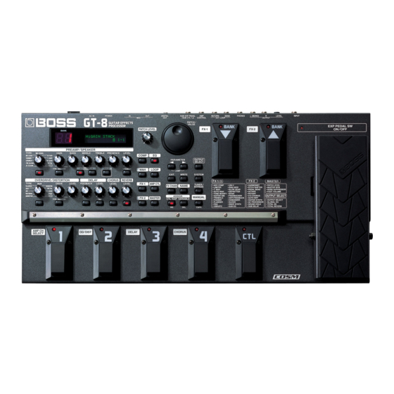
Page 4: Location Of Controls
Dec.2004 GT-8 LOCATION OF CONTROLS fig.haichi.eps 10.11.12. 15.16.14. 17.19. 1.2. 4. 5. 7. 8. 1.3. 13.14. 17.18. 20. 21.22. 30.31.32.33. 35.36.37.38. 39.40.41. 50.51. 42.43. 45.46. -
Page 5: Location Of Controls Parts List
Dec.2004 LOCATION OF CONTROLS PARTS LIST PART CODE CATEGORY PART NAME DESCRIPTION Q'TY G2477122 KNOB,BUTTON R-KNOB F3279803 POTENTIOMETER POTENTIOMETER 11 CLICKS 50KB RD901-40-125F-B54-11D F3279802 POTENTIOMETER POTENTIOMETER NO CLICK 50KB RD901-40-125F-B54-00D G2237113 MISCELLANEOUS GUARD PLATE G2237112 MISCELLANEOUS GUARD 75D912C000 CASING TOP COVER F5029412 DISPLAY UNIT 7SEG LED... - Page 6 GT-8...
-
Page 7: Exploded View
Dec.2004 GT-8 EXPLODED VIEW fig.bunkai.eps... -
Page 8: Exploded View Parts List
Dec.2004 EXPLODED VIEW PARTS LIST [Parts] PART CODE PART NAME DESCRIPTION Q’TY 75D912C000 TOP COVER 75D912E000 BOTTOM COVER G2237112 GUARD G2237113 GUARD PLATE G2637107 RUBBER SW G2567121 RUBBER SW ESCUTCHEON G2357120 FOOT G2567119 DISPLAY COVER 12499175 BUTTON JSPUE001A F2477101 DR-KNOB 01340412 P R-KNOB SF-A BLK/LCG... -
Page 9: Wiring Diagram
GT-8 WIRING DIAGRAM fig.haisen.eps WIRING 12P SW2 BOARD ASSY WIRING 7P WIRING 13P WIRING 8P RIBBON 7P SW3 BOARD SW1 BOARD ASSY ASSY RIBBON 3P ENC BOARD ASSY EXP BOARD ASSY WIRING 3P MAIN SHEET ASSY WIRING DIAGRAM PARTS LIST PART CODE PART NAME DESCRIPTION... -
Page 10: Parts List
Dec.2004 PARTS LIST fig.part1e Due to one or more of the following reasons, SAFETY PRECAUTIONS: parts with parts code ******** cannot be supplied as service parts. The parts marked have safety-related characteristics. Use only listed parts for replacement. • Part supplied only as a component in a complete assembly •... - Page 11 GT-8 F5249101 HD74HC4051P IC (CMOS) IC4,IC6 F5249134 TC74HC08AF IC (CMOS) IC26 on MAIN F5279720 TC74VHC138F IC (CMOS) IC13 on MAIN F5249128 TC74VHC574FT(EL) IC (CMOS) IC11,IC14 on MAIN F5249129 TC74VHCT574AF IC (CMOS) IC12,IC15 on MAIN F5279311 TC7SH04F IC (CMOS) IC28 on MAIN F5249135 TC7SH04FU IC (CMOS)
- Page 12 Dec.2004 RESISTOR F5399128 1K J MTL.FILM RESISTOR R22,R23,R33,R34,R60,R61,R80,R84,R110,R1 21,R160,R161,R162 on MAIN F5399200 1M J MTL.FILM RESISTOR R7 on MAIN F5399130 2.2K J MTL.FILM RESISTOR R70,R123 on MAIN F5399190 220K J MTL.FILM RESISTOR R50 on MAIN F5399118 MTL.FILM RESISTOR R26,R40,R75 on MAIN F5399107 MTL.FILM RESISTOR R113 on MAIN...
-
Page 13: Hex Button Feni
GT-8 CONNECTOR F3439164 A2001WR2-8P CONNECTOR 8P CN3 on MAIN WIRING, CABLE F3467038 WIRING 12P P=2MM L=120MM CN5 on SW F3467039 WIRING 13P P=2MM L=65MM CN8 on SW G3467178 WIRING 8P P=2MM L=65MM CN7 on SW G3477156 RIBBON CABLE 7P P=2MM L=140MM CN3,CN2 on SW G3467175 WIRING... - Page 14 Dec.2004 ACCESSORIES (Standard) G6047001 OWNER’S MANUAL JAPANESE G6047002 OWNER’S MANUAL ENGLISH G6027107 PRESET PATCH LIST JAPANESE/ENGLISH G6047005 READ ME FIRST JAPANESE/ENGLISH G6027108 USER PATCH LIST JAPANESE/ENGLISH 40232389 WARRANTY CARD FOR BOSS JAPAN ONLY...
-
Page 15: Checking The Version Number
GT-8 CHECKING THE VERSION When Transmitting Data to Another GT-8 NUMBER Connect as shown in the figure below, and match the Device ID for the transmitting and receiving devices. fig.08-150 Simultaneously hold down the [OUTPUT SELECT], [TUNER] and [MANUAL] buttons and turn on the power to the GT-8. The version number and checksum appear in the lower row of the LCD display. -
Page 16: Factory Reset Instructions
Dec.2004 Receiving Data from an External fig.08-220d MIDI Device (Bulk Load) Making the Connections At this stage, even more data can be received. Press [EXIT] to quit Bulk Load. When Receiving Data Saved on a MIDI After you press [EXIT], “Checking...” appears in the display, indicating Sequencer that the GT-8 is checking the received data. -
Page 17: System Software Updating Instructions
GT-8 SYSTEM SOFTWARE After the GT-8 has received all of the SMF data, a checksum (4-digit number) of the system software is run; confirm the checksum value. UPDATING INSTRUCTIONS fig.4-01up All Completed. Sum=**** Required Equipment • Sequencer (MC-80 or other) TEST MODE •... - Page 18 Dec.2004 Quitting Test Mode [3] Seven-Segment LEDs Confirm that the segments in the seven-segment LEDs go off one at a time each time [WAH] is pressed. Power off the unit. All of the segments should be off after the [WAH] button is pressed 14 DSP Check times.
- Page 19 GT-8 7. Battery that the waveform alternately changes as shown below. Press the [WRITE] button; the voltage of the memory backup battery is displayed. fig.7-01test <--> 7.Battery 3.1V Error indications: “*.*V Low”: When the battery voltage is 2.0-2.6 V. Connect the oscilloscope (Channel 1 and 2) to the PHONES jack, and use the “No Battery!!”: When there is no battery, or when the battery voltage is below same procedure to confirm the waveform output.
- Page 20 Dec.2004 12. INPUT A/D 15. Noise(LOOP) Input a rectangular wave, and observe the output waveform with the INPUT -> A/D -> DSP -> D/A -> SEND -> RETURN -> A/D -> DSP -> D/A - oscilloscope. > OUTPUT INPUT: Rectangular wave, 400 Hz, 40 mVp-p (Connect noise meter and observe) Press the [WRITE] button.
- Page 21 GT-8 17. Factory Load Press the [WRITE] button; the following is displayed. fig.17-01test 17.Factory Load press [WRITE] Press the [WRITE] button again. fig.17-02test 17.Factory Load sure? Press the [WRITE] button again to execute Factory Reset. fig.17-03test Now writing... When Factory Reset is completed, the following is displayed. fig.17-04test 17.Factory Load Press the [EXIT] button to return to the normal operating mode.
-
Page 22: Block Diagram
Dec.2004 BLOCK DIAGRAM fig.block.eps MIDI IN / OUT EXP BOARD ASSY PEDAL VR SUB EXP PEDAL IC22 CPU / SUB CTL 1, 2 H8S/2312S ENC BOARD ASSY IC37 ENCODER JK10 PHOTO RELAY AMP CONTROL TLP172A IC2a SW1 BOARD ASSY INPUT PANEL SW, LED IC1a IC2b... - Page 23 GT-8...
-
Page 24: Circuit Board (Main Sheet)
Dec.2004 GT-8 CIRCUIT BOARD (MAIN SHEET) fig.b-main1.eps View from components side... - Page 25 Dec.2004 GT-8 fig.b-main2.eps View from foil side...
-
Page 26: Circuit Diagram (Main Sheet 1/3) (Power)
Dec.2004 GT-8 CIRCUIT DIAGRAM (MAIN SHEET 1/3) (Power) fig.c-main-power.eps IC30 R118 BA17805FP IC31 10 (0805size) S-812C33AY-Z 1N4004 C150 C151 C154 C155 C152 C153 C156 R119 N.I.U. 47/16 N.I.U. 1.5k C149 R157 470/35 N.I.U.(miniSMDC075) SW1A R120 R121 SDKLA1-B N.I.U.(1/2W) R123 JK11 DSS9ND31H223Q91J L16 N.I.U.(0) 2.2k... -
Page 27: Circuit Diagram (Main Sheet 2/3) (Jack)
Dec.2004 GT-8 CIRCUIT DIAGRAM (MAIN SHEET 2/3) (Jack) fig.c-main-jack.eps 0.01 1.2k N.I.U C3 10P C196 N.I.U. N.I.U R4 12K(F) 47/16 R5 100K(F) IC2A AK4552VT N.I.U.(0) 1SS352 NJM2100M N.I.U.(0) C170 MCLK N.I.U IC1A C171 GUITAR_IN SDTO GUITAR IN M5238FP N.I.U BCLK C172 0.47(ECPU1C474MA5) LRCK... -
Page 28: Circuit Diagram (Main Sheet 2/3) (Digital)
Dec.2004 GT-8 CIRCUIT DIAGRAM (MAIN SHEET 2/3) (Digital) fig.c-main-digital.eps D 3. 3 D 3. 3 IC39 R133 R151 TC7SH04FU N.I.U.(0) N.I.U D 3. 3 D 3. 3 AD_C TO LCD AD_B CRN34103J CRN34103J AD_A R134 SW_SCAN4 C198 SW_SCAN3 A2541WR2-2A16NP SW_SCAN2 SW_SCAN1 CRN34101J SW_SCAN0... -
Page 29: Circuit Board (Sw Sheet)
Dec.2004 GT-8 CIRCUIT BOARD (SW SHEET) fig.b-sw.eps View from components side... -
Page 30: Circuit Diagram (Sw Sheet)
Dec.2004 GT-8 CIRCUIT DIAGRAM (SW SHEET) fig.c-sw.eps BANK BANK EXP PEDAL FX "1" "2" "3" "4" "CTL" DOWN ON/OFF D 3. 3 D 3. 3 D 3. 3 D 3. 3 D 3. 3 EXP BOARD D 3. 3 D 3. 3 D 3. -
Page 31: Error Messages
Dec.2004 ERROR MESSAGES If you attempt an incorrect operation or if an operation could not be executed, the display will indicate an error message. Refer to this list and take the appropriate action. fig.09-080d ● The memory backup battery inside the GT-8 has run down. (This message will appear when the power is turned on.) ❍...
Need help?
Do you have a question about the Roland GT-8 and is the answer not in the manual?
Questions and answers