Table of Contents
Advertisement
Advertisement
Table of Contents

Related Manuals for Nordic nRF52833 DK


Summary of Contents for Nordic nRF52833 DK
- Page 1 DK User Guide v1.0.1 4452_198 v1.0.1 / 2020-04-08...
-
Page 2: Table Of Contents
....... . . Nordic tools and downloads ...... - Page 3 9.3 Using an ampere-meter for current measurement ....RF measurements ....... Glossary .
-
Page 4: Revision History
Revision history Date Version Description April 2020 1.0.1 Editorial changes October 2019 First release (for nRF52833 DK v0.9.0 and 1.0.0) 4452_198 v1.0.1... -
Page 5: Introduction
Introduction The nRF52833 DK is a Development Kit (DK) that includes hardware, firmware source code, documentation, hardware schematics, and layout files. This kit can be used for developing for either the nRF52833 or nRF52820 System on Chip (SoC)s. The key features of the DK are: ®... -
Page 6: Minimum Requirements
Minimum requirements Before you start, check that you have the required hardware and software. Hardware requirements • Personal computer (PC) or Mac • Micro-USB 2.0 cable Software requirements • SEGGER J-Link Software v6.52 or later 4452_198 v1.0.1... -
Page 7: Kit Content
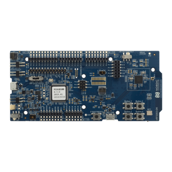
The nRF52833 DK includes hardware, preprogrammed firmware, documentation, hardware schematics, and layout files. 3.1 Hardware content The nRF52833 DK (PCA10100) comes with a Near Field Communication (NFC) antenna. Figure 1: nRF52833 DK (PCA10100) and NFC antenna Hardware files The hardware design files including schematics, PCB layout files, bill of materials, and Gerber files for the... - Page 8 Kit content Nordic documentation • nRF52833 DK Getting Started • nRF52833 Product Specification • Software Development Kit • nRF52833 Compatibility Matrix • nRF52833 Engineering A Errata 4452_198 v1.0.1...
-
Page 9: Getting Started
Getting started To get started with the nRF52833 DK, go to nRF52833 DK Getting Started and follow the instructions there. 4452_198 v1.0.1... -
Page 10: Nordic Tools And Downloads
SEGGER Embedded Studio (SES) MDK-ARM Keil µVision GNU/GCC SES is the recommended platform. It is free for use with nRF devices. Essential tools You need to download these Nordic tools to develop with our devices. Tool Description Download Documentation Protocol... - Page 11 Nordic tools and downloads Tool Description Download Documentation Protocol SoftDevice Wireless protocol BLE/ANT Compatible downloads nRF51 SoftDevice stack for nRF52840 Specifications Compatible downloads nRF52 SoftDevice for nRF52833 Specifications Compatible downloads for nRF52832 Compatible downloads for nRF52811 Compatible downloads for nRF52810...
- Page 12 Nordic tools and downloads Tool Description Download Documentation Protocol network to the Internet See also Nordic mobile apps for a list of available Bluetooth Low Energy and Mesh mobile apps for iOS, Android, and Windows Phones. 4452_198 v1.0.1...
-
Page 13: Start Developing
Start developing After you have set up the DK and installed the toolchain, it is time to start developing. There are several ways to continue from here, depending on which networking protocol you want to use. • For nRF5 SDK for Bluetooth Low Energy, ANT, or proprietary 2.4Ghz (nRF5 Series devices), see nRF5 SDK Getting Started. -
Page 14: Interface Mcu
Interface MCU The interface MCU on the nRF52833 DK runs SEGGER J-Link OB interface firmware and is used to program and debug the firmware of the nRF52833 SoC. Figure 2: Interface MCU 7.1 IF Boot/Reset button The nRF52833 DK is equipped with an IF Boot/Reset button (SW5). -
Page 15: Msd
Interface MCU The virtual COM port has the following features: • Flexible baud rate setting up to 1 Mbps. • Dynamic Hardware Flow Control (HWFC) handling. • Tri-stated UART lines when no terminal is connected. The table below shows an overview of the UART connections on the nRF52833 SoC and the interface MCU. GPIO nRF52833 nRF52833 UART P0.05... -
Page 16: Hardware Description
Hardware description The nRF52833 DK (PCA10100) can be used as a development platform for the nRF52833 SoC. It features an onboard programming and debugging solution. In addition to radio communication, the SoC can communicate with a computer through USB and a virtual COM port provided by the interface MCU. -
Page 17: Power Supply
Debug in supply Figure 5: Block diagram 8.3 Power supply The nRF52833 DK has multiple power options. The power options are: • USB connector J2 for the interface MCU (5 V) • USB connector J3 for the nRF52833 SoC (5 V) •... -
Page 18: Power Sources
Hardware description Figure 7: Power supply options (back) 8.3.1 5 V power sources The nRF52833 DK has a 5 V boost regulator. It gives a stable 5 V output from four possible sources: • USB connector J2 for the interface MCU •... - Page 19 Hardware description If the high voltage regulator of the nRF52833 is used, the DK will be supplied from the VDD_nRF voltage follower regardless of the state of the other power sources. 4452_198 v1.0.1...
- Page 20 Hardware description Figure 9: Power supply circuitry 4452_198 v1.0.1...
-
Page 21: Interface Mcu Power
Hardware description The power switches work in the way that the body diode of the internal transistor powers the VSUPPLY net, which supplies the gates controlling the enable signal of the switches. If 5 V is present, the switches for external supply and battery are disabled. If external supply is present, the switch for the battery is disabled. -
Page 22: Nrf52833 Power Source
Operating modes on page 24 for more information. 8.3.4 nRF52833 power source The nRF52833 DK has a power source switch (SW9) for selecting between three power sources for the nRF52833 SoC. The three positions of the switch are: • VDD (default) •... -
Page 23: Nrf52833 Soc Direct Supply
Hardware description In the Li-Po position, the high voltage regulator of the SoC is supplied directly from the Li-Po battery connectors (J6 or P27). In the USB position, the USB high voltage regulator gets power from the nRF52833 USB connector (J3). When the high voltage regulator is used, the VDD_nRF voltage can be set by the firmware of the SoC. -
Page 24: Operating Modes
24. 8.4 Operating modes The nRF52833 DK has various modes of operation. 8.4.1 USB detect To detect when USB for the interface MCU is connected, there is a circuit sensing the VBUS of USB connector J2. -
Page 25: Signal Switches
Hardware description Figure 16: nRF ONLY switch (SW6) 8.4.3 Signal switches On the nRF52833 DK, there are multiple analog switches that are used to connect and disconnect signals based on different scenarios. 4452_198 v1.0.1... - Page 26 Hardware description Figure 17: Signal switches The USB and SW6 control the signal switches by using USB_DETECT as an input to SW6. Therefore, the interface MCU can be disconnected either by unplugging the USB cable from J2 or by toggling the nRF ONLY switch (SW6).
-
Page 27: Connector Interface
31 for more information. 8.5 Connector interface Access to the nRF52833 GPIOs is available from connectors P2, P3, P4, P5, P6, and P24. The P1 connector provides access to ground and power on the nRF52833 DK. 4452_198 v1.0.1... - Page 28 Some of the signals are also available on connectors P7, P8, P9, P10, P11, and P12, which are on the bottom side of the DK. By mounting pin lists on the connector footprints, the nRF52833 DK can be used as a shield for Arduino motherboards or other boards that follow the Arduino standard.
-
Page 29: Mapping Of Analog Pins
AIN2 P0.28 AIN4 P0.29 AIN5 P0.30 AIN6 P0.31 AIN7 Table 3: Mapping of analog pins 8.6 Buttons and LEDs The four buttons and four LEDs on the nRF52833 DK are connected to dedicated GPIOs on the nRF52833 SoC. 4452_198 v1.0.1... - Page 30 Hardware description Part GPIO GPIO alternative Solder bridge Button 1 P0.11 P1.07 Button 2 P0.12 P1.08 Button 3 P0.24 Button 4 P0.25 LED 1 P0.13 LED 2 P0.14 LED 3 P0.15 LED 4 P0.16 Table 4: Button and LED connection If P0.13–P0.16 are needed elsewhere, the LEDs can be disconnected by cutting the short on SB5–SB8, see figure Figure 21: Disconnecting the LEDs...
-
Page 31: Khz Crystal
The nRF52833 SoC can use an optional 32.768 kHz crystal (X2) for higher accuracy and lower average power consumption. On the nRF52833 DK, P0.00 and P0.01 are used for the 32.768 kHz crystal by default and are not available as GPIO on the connectors. -
Page 32: Debug Output
VDD by cutting SB60 and soldering SB59. 8.9 Debug output The nRF52833 DK supports programming and debugging external boards with nRF51 or nRF52 SoCs. To debug an external board with SEGGER J-Link OB IF, connect to the Debug out connector (P19) with a 10- pin cable. -
Page 33: Connectors For Programming External Boards
P19. If it is inconvenient to have a separate power supply on the external board, the nRF52833 DK can supply power through the Debug out connector (P19). To enable this, short solder bridge SB47. Note that as long as SB47 is shorted, it is not possible to program the onboard nRF52833 SoC even if the external board is unplugged. -
Page 34: Extra Op-Amp
Hardware description Pin number Signal Description EXT_VTG Voltage supply from the external target, used as voltage detect input to the interface EXT_SWDIO Serial Wire Debug (SWD) data line Ground EXT_SWDCLK SWD clock line Ground EXT_SWO Serial Wire Output (SWO) line N.C. -
Page 35: Nfc Antenna Interface
17. Figure 27: Extra op-amp 8.11 NFC antenna interface The nRF52833 DK supports an NFC tag. NFC-A listen mode operation is supported on the nRF52833 SoC. The NFC antenna input is available on connector J5 on the nRF52833 DK. -
Page 36: Solder Bridge Configuration
Figure 29: NFC input 8.12 Solder bridge configuration The nRF52833 DK has a range of solder bridges for enabling or disabling functionality on the DK. Changes to these are not needed for normal use on the DK. The following table is a complete overview of the solder bridges on the nRF52833 DK. - Page 37 Hardware description Solderbridge Default Function SB42 Closed Cut to disconnect IF Boot/Reset button from nRF52833 reset pin when the interface MCU is disconnected SB43 Open Short to connect IF Boot/Reset button to RESET pin on the Arduino interface SB44 Open Short to connect the RESET pin on the Arduino interface to the nRF52833 reset pin SB45...
-
Page 38: Measuring Current
Measuring current The current drawn by the nRF52833 SoC can be monitored on the nRF52833 DK. Current can be measured using various test instruments. Examples of test equipment are the following: • Power analyzer • Oscilloscope • Ampere-meter • Power Profiler Kit Power analyzer and Power Profiler Kit measurements will not be described in the present document. -
Page 39: Using An Oscilloscope For Current Profile Measurement
Measuring current Figure 30: Preparing the for current measurements • To put P22 in series with the load, cut the PCB track shorting solder bridge SB40. • To restore normal kit function after measurement, solder SB40 or apply a jumper on P22. 9.2 Using an oscilloscope for current profile measurement An oscilloscope can be used to measure both the average current over a given time interval and capture... -
Page 40: Using An Ampere-Meter For Current Measurement
Measuring current Some tips to reduce noise: • Use probes with 1 × attenuation • Enable averaging mode to reduce random noise • Enable high resolution function if available Use a minimum of 200 kSa/s (one sample every 5 µs) to get the correct average current measurement. 9.3 Using an ampere-meter for current measurement The average current drawn by the nRF52833 SoC can be measured using an ampere-meter. -
Page 41: Rf Measurements
RF measurements The nRF52833 DK is equipped with a small coaxial connector (J1) for conducting measurements of the RF signal using a spectrum analyzer. The connector is of SWF type (Murata part no. MM8130-2600) with an internal switch. By default, when no cable is attached, the RF signal is routed to the onboard trace antenna. -
Page 42: Glossary
Glossary Clear to Send (CTS) In flow control, the receiving end is ready and telling the far end to start sending. Data Terminal Ready (DTR) A control signal in RS-232 serial communications transmitted from data terminal equipment, such as a computer, to data communications equipment. Development Kit (DK) A development platform used for application development. - Page 43 System on Chip (SoC) A microchip that integrates all the necessary electronic circuits and components of a computer or other electronic systems on a single integrated circuit. Transmit Data (TXD) A signal line in a serial interface that transmits data to another device. 4452_198 v1.0.1...
-
Page 44: Acronyms And Abbreviations
Acronyms and abbreviations These acronyms and abbreviations are used in this document. Clear to Send Development Kit Data Terminal Ready HWFC Hardware Flow Control Integrated Development Environment Mass Storage Device Near Field Communication op-amp Operational Amplifier Root Mean Square Request to Send Receive Data SubMiniature version A System on Chip... -
Page 45: Legal Notices
Nordic Semiconductor ASA customers using or selling these products for use in such applications do so at their own risk and agree to fully indemnify Nordic Semiconductor ASA for any damages resulting from such improper use or sale.
Need help?
Do you have a question about the nRF52833 DK and is the answer not in the manual?
Questions and answers