Table of Contents
Advertisement
Quick Links
Struck Documentation
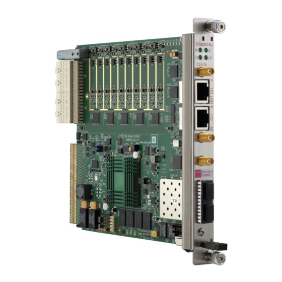
SIS8300-KU
MTCA.4 Digitizer
SIS8300-KU
10 channel
125 MSPS 16-bit
MTCA.4 Digitizer
User Manual
SIS GmbH
Harksheider Str. 102A
22399 Hamburg
Germany
Phone: ++49 (0) 40 60 87 305 0
Fax:
++49 (0) 40 60 87 305 20
email: info@struck.de
http://www.struck.de
Version: SIS8300KU-M-x002-1-V101.doc as of 09.03.2017
Page 1 of 92
Advertisement
Table of Contents

Related Manuals for SIS SIS8300-KU

Summary of Contents for SIS SIS8300-KU
- Page 1 Struck Documentation SIS8300-KU MTCA.4 Digitizer SIS8300-KU 10 channel 125 MSPS 16-bit MTCA.4 Digitizer User Manual SIS GmbH Harksheider Str. 102A 22399 Hamburg Germany Phone: ++49 (0) 40 60 87 305 0 Fax: ++49 (0) 40 60 87 305 20 email: info@struck.de http://www.struck.de...
- Page 2 Struck Documentation SIS8300-KU µTCA 16-bit Digitizer Revision Table: Revision Date Modification 0.01 24.10.2016 Based on SIS8300L2-M-x00D-1-V110 (Firmware: V100D) 0.02 25.10.2016 Chapter "Functionality" updated Chapter "Block diagram" updated Chapter "Platform Management" MMC scheme updated Chapter "MGT clock" scheme updated Chapter "Frontpanel" sketch updated Chapter 5.1 changed from Harlink to "RJ45 In-/Outputs"...
-
Page 3: Table Of Contents
Struck Documentation SIS8300-KU MTCA.4 Digitizer - Table of contents Table of contents ............................. 3 Introduction ..............................5 Related documents ..........................5 Design ................................6 Functionality ............................6 Block Diagram ............................6 Platform Management ..........................7 2.3.1 E-Keying ............................7 2.3.2 MMC sensors .......................... - Page 4 Struck Documentation SIS8300-KU µTCA 16-bit Digitizer 7.5.15 DAC Trigger Control register ....................... 43 Synch-Mode = 1: Both DACs are triggered synchronous with DAC1 “Start-logic” ........43 7.5.16 Clock Distribution Multiplexer control register ................44 7.5.17 Clock Distribution AD9510 Serial Interface (SPI) interface register ..........46 7.5.18...
-
Page 5: Introduction
The SIS8300-KU is a 10 channel 125 MS/s digitizer with 16-bit resolution according to the MTCA.4 standard. SIS8300-KU Note: While the SIS8300-KU is Kintex Ultrascale based you will find many Virtex 5/6 references in the firm- and software for historical reasons (i.e. remnants from the SIS8300_V2 and SIS8300L2 designs). -
Page 6: Design
SIS8300-KU MTCA.4 Digitizer 2 Design The central building block of the SIS8300-KU card is a Xilinx Kintex Ultrascale FPGA. It holds the 4 lane PCI Express interface and is in control of all active components. 2.1 Functionality The key properties of the SIS8300-KU card are listed below. -
Page 7: Platform Management
MMC as FRU information. It will be communicated to the MCH at power up. E-Keying entries in the FRU information of the SIS8300-KU match the FPGA design at shipment version and are fixed. If you change the FPGA design and/or make a custom FPGA design it can be necessary to change part of the FRU information also. -
Page 8: Mmc Sensors
An additional memory with unique ID is available for board identification purposes. An overview of all existing SIS8300-KU MMC sensors –as seen with NATView- is illustrated below. Note: On SIS8300-KU further temperature sensors exist, please see section 2.6. -
Page 9: Spi Connectivity
The SPI bus connectivity scheme of the SIS8300-KU is illustrated below. The SIS8300-KU has two SPI EEPROMs, that can hold FPGA configuration data. So it is possible to choose from two firmware designs for the configuration of the FPGA. The selection of the SPI EEPROM is under control of the MMC and can be changed per IPMI command. -
Page 10: Jtag Connectivity
SIS8300-KU MTCA.4 Digitizer JTAG Connectivity The JTAG connectivity scheme of the SIS8300-KU is illustrated below. JTAG connection to µRTM can be realized in FPGA firmware but is a optional feature for future. Switching connection of FPGA hardware JTAG port between MTCA (AMC Backplane) and on board JTAG connector (illustrated switch CON/MTCA) can be made via IPMI command. -
Page 11: Dac
A software example can be found on the Struck product DVD under: sisdvd_xxxxxx\sis8xxx and DWC\sis8300L\software\tests\adc_temp A part of the SIS8300-KU versions comes with the 250 MSPS MAX5878 dual DAC chip. The dual DAC can be used to control the Vectormodulator on the DWC8VM1 Downconverter/Vectormodulator RTM over the Zone 3 connector for example. -
Page 12: Clock Distribution
Struck Documentation SIS8300-KU MTCA.4 Digitizer Clock Distribution 2.8.1 Overall Clock Distribution The clock distribution scheme of the SIS8300-KU is illustrated below. FPGA Quartz CLK69 (optional) ΔT ΔT SI5326 RJ45 FPGA CLK05 MUX C ΔT ΔT ADCLK925 ADCLK925 MUX A MUX B... -
Page 13: Dac Clock
Struck Documentation SIS8300-KU MTCA.4 Digitizer 2.8.2 DAC Clock The DAC clock scheme of the SIS8300-KU is illustrated below. 16 DATA DAC_SELIQ FPGA FPGA_FB FPGA_CLK DAC_CLK DIV1_OUT0 RTM_CLK4 ΔT ΔT DIV0_OUT0 ΔT ΔT 2.8.3 µRTM Clock Overview The µRTM clock overview table is shown below. -
Page 14: Amc_Tclk On Zone 3
The status can be read back with the command: <IPMI> raw 0x30 0x02 After power up TCLKA is selected per default. AMC_TCLK signal is available for SIS8300-KU with Zone 3 class compatibility A1.1CO and A1.0C only. Please refer to section 10.4.2. Page 14 of 92... -
Page 15: Mgt Clock
Struck Documentation SIS8300-KU MTCA.4 Digitizer 2.8.6 MGT Clock The MGT (Multi Gigabit Transceiver) clock scheme of the SIS8300-KU is illustrated below. DIV1_OUT1 clock from AMC Backplane (FCLKA) ΔT ΔT 227-0 PCIe 3 (Port 7) REFCLK0 227-1 PCIe 2 (Port 6) -
Page 16: Jumper/Connector Pin Assignments
CON100 is a 2mm (i.e. metric) 14 pin header that allows you to reprogram the firmware of the SIS8300-KU board with a JTAG programmer. The pin out is shown in the schematic below. It is compatible with the cable that comes with the XILINX HW-USB-II-G-JTAG platform cable. -
Page 17: J32 Avr Jtag
This 10-pin header is used to connect to the JTAG of the Atmel ATxmega128 microcontroller providing the IPMI/MCH functionality of the SIS8300-KU. J32 can be found at the left bottom side of the board. The pin out is shown in the schematic below. -
Page 18: Leds
SFP Link 2 receiver loss of signal T (L2) SFP Link 2 transmitter fault Note: if SIS8300-KU is in operational state and no SFP modules are present in SFP card cage associated LEDs (R and T) are lit permanently Page 18 of 92... -
Page 19: Smd Leds
Struck Documentation SIS8300-KU MTCA.4 Digitizer 4.3 SMD LEDs A number of surface mount red LEDs are on the SIS8300-KU to visualize part of the board status. LED designator LED comment Function D20A Firmware dependent (Optical Link 1 up) D20B Firmware dependent... -
Page 20: Front Panel
Struck Documentation SIS8300-KU MTCA.4 Digitizer 5 Front panel A sketch of the SIS8300-KU front panel view (with front panel I/O option) is shown below. Page 20 of 92... -
Page 21: Rj45 Lvds In-/Outputs
Struck Documentation SIS8300-KU MTCA.4 Digitizer 5.1 RJ45 LVDS In-/Outputs Two identical RJ45 connectors are present for clock and digital I/O signals. A drawing with the pin count and pin orientation is shown below. Front view The RJ45 Input connector has inputs only and RJ45 Output connector has outputs res- pectively. -
Page 22: Sma Clock Input
Struck Documentation SIS8300-KU MTCA.4 Digitizer 5.2 SMA Clock Input The front panel SMA clock input is designed to accept a maximum peak to peak signal level of 3V into 50 Ohms. The clock input signal is coupled to the internal logic via a capacitor. -
Page 23: Board Layout
µRTM Keying TYCO 5120913-3 (*) J209 Data & Clock Out ERNI 133268 J205 Data & Clock In ERNI 133268 J604 Watchdog SAMTEC HTSW-102-26-G-S Note : The used Key may depend on the hardware configuration of the SIS8300-KU Page 23 of 92... -
Page 24: Firmware Description
Struck Documentation SIS8300-KU MTCA.4 Digitizer 7 Firmware Description 7.1 ADC Sample Logic The block diagram shows the ADC data handling. Each ADC channel has its own Memory Address Control Logic. Page 24 of 92... -
Page 25: Memory Interface
Write Interface addr sis_write_addr_fifo_wr_en protocol sis_write_64bit_addr_fifo_din Address Fifo 512 x 32 sis_write_addr_fifo_wr_count Data sis_write_data_fifo_wr_en sis_write_data_fifo_din Data Fifo 512 x 512 sis_write_data_fifo_wr_count Note: the data width has changed from 256 bit to 512 bit with the SIS8300-KU. Page 25 of 92... -
Page 26: Memory Write Interface
Therefore the lower 3 address bits of the written 64-bit address must be 0 and the “next address” will be incremented by 8. Note again: the data width has changed from 256 bit to 512 bit with the SIS8300-KU and therefore the logic has to write in packages of 512 bits (64 Bytes) into the memory. -
Page 27: Memory Buffer
Start Address (see Memory Sample Start Block Address register) and the Sample Length (see Sample Block Length register). Note again: the data width has changed from 256 bit to 512 bit with the SIS8300-KU and therefore only even “Block addresses” and even “Block length” values are valid. -
Page 28: Address Map
ADC Input Tap delay register 0x4E DAC Trigger and DAC_CLK Prescaler setup register 0x4F DAC RAM endpoint register 0xFF Bit 0 = 1: Master Reset (reset all registers) Notes 1: new with SIS8300-KU 2: changed from SIS8300L/L2 to SIS8300-KU Page 28 of 92... - Page 29 Struck Documentation SIS8300-KU MTCA.4 Digitizer Offset Access Function Note 0x100 ADC ch1 Trigger Setup register 0x101 ADC ch2 Trigger Setup register 0x109 ADC ch10 Trigger Setup register 0x110 ADC ch1 Trigger Threshold register 0x111 ADC ch2 Trigger Threshold register 0x119...
-
Page 30: Register Description
0000FF00 Firmware Revision 1..255 000000FF Example: The initial versions of the SIS8300-KU reads 0x83031001 and 0x83032001 Meaning of the several firmware versions: 83031xxx: standard versions (for RTM8900) 83032xxx: versions with µRTM-USER-I²C support on Zone 3 Connector J30 4a/b (DWCnnnn) 7.5.2 Serial Number register... -
Page 31: User Control/Status Register
Struck Documentation SIS8300-KU MTCA.4 Digitizer 7.5.3 User Control/Status register #define SIS8300_USER_CONTROL_STATUS_REG 0x04 The control register is implemented as a selective J/K register, a specific function is enabled by writing a 1 into the set/enable bit, the function is disabled by writing a 1 into the clear/disable bit (which location is 16-bit higher in the register). -
Page 32: Firmware Options Register
Struck Documentation SIS8300-KU MTCA.4 Digitizer 7.5.4 Firmware Options register #define SIS8300_FIRMWARE_OPTIONS_REG 0x05 This register holds the information of the Xilinx firmware option features. read Function reserved Hardware Version flag reserved reserved reserved reserved reserved reserved reserved Z3 Class Bit 1... -
Page 33: Adc Temperature Sensor Interface Register
Struck Documentation SIS8300-KU MTCA.4 Digitizer 7.5.5 ADC Temperature Sensor interface register #define SIS8300_ADC_TEMP_I2C_REG 0x06 Write read unused Write/Read Logic BUSY Flag unused unused unused unused unused unused unused Byte Read cycle Byte Write cycle Issue STOP condition Issue REPEATSTART condition Issue START condition Master I²C ACK bit, written during reads... -
Page 34: Firmware Options Register
Struck Documentation SIS8300-KU MTCA.4 Digitizer 7.5.6 Firmware Options register #define SIS8300KU_PCIE_STATUS_REG 0x07 This register holds the information of the PCI Express Link. read Function reserved reserved reserved PCI Express Link Max_Payload_Size bit 2 PCI Express Link Max_Payload_Size bit 1 PCI Express Link Max_Payload_Size bit 0... -
Page 35: Adc Acquisition Control/Status Register
Struck Documentation SIS8300-KU MTCA.4 Digitizer 7.5.7 ADC Acquisition Control/Status register #define SIS8300_ACQUISITION_CONTROL_STATUS_REG 0x10 write read Status: DDR4 Memory Init OK Status: internal Sample Logic Buffer FIFO Not Empty Status: internal Sample Logic Busy ‘1’ : Disable Sampling (Reset Sample Logic) ‘1’... -
Page 36: Adc Sample Control Register
Struck Documentation SIS8300-KU MTCA.4 Digitizer 7.5.8 ADC Sample Control register #define SIS8300_SAMPLE_CONTROL_REG 0x11 ADC channels can be disabled from storing data to memory by setting the corresponding disable bit in this register. write Enable external Trigger Enable internal Trigger Disable Sampling Ch10... -
Page 37: Mlvds Input/Output Control Register
Struck Documentation SIS8300-KU MTCA.4 Digitizer 7.5.9 MLVDS Input/Output Control register #define SIS8300_MLVDS_IO_CONTROL_REG 0x12 Write Read Enable LVDS Output Bit 7 Enable LVDS Output Bit 7 Enable LVDS Output Bit 6 Enable LVDS Output Bit 6 Enable LVDS Output Bit 1... -
Page 38: Rj45 Connector Input/Output Control Register
Struck Documentation SIS8300-KU MTCA.4 Digitizer 7.5.10 RJ45 Connector Input/Output Control register #define SIS8300KU_RJ45_IO_CONTROL_REG 0x13 Write Read No function No function No function Test Output Enable (**) Test Output Enable Test Output 3 (*) Test Output 3 Test Output 2 (*) -
Page 39: Sfp1 Link Control/Status Register
Struck Documentation SIS8300-KU MTCA.4 Digitizer 7.5.11 SFP1 Link Control/Status register #define SIS8300KU_SFP1_LINK_CONTROL_STATUS_REG 0x14 Write Read SFP1 and SFP2 GTH reset pulse DMA Output Fifo full Flag DMA Output Fifo halffull Flag DMA Output Fifo empty Flag DMA Input Fifo read count D9... -
Page 40: Sfp2 Link Control/Status Register
Struck Documentation SIS8300-KU MTCA.4 Digitizer 7.5.12 SFP2 Link Control/Status register #define SIS8300KU_SFP2_LINK_CONTROL_STATUS_REG 0x15 Write Read DMA Output Fifo full Flag DMA Output Fifo halffull Flag DMA Output Fifo empty Flag DMA Input Fifo read count D9 DMA Input Fifo read count D0... -
Page 41: Port12 Link Control/Status Register
Struck Documentation SIS8300-KU MTCA.4 Digitizer 7.5.13 Port12 Link Control/Status register #define SIS8300KU_PORT12_LINK_CONTROL_STATUS_REG 0x16 Write Read Port12,13,14 and 15 GTH reset pulse DMA Output Fifo full Flag DMA Output Fifo halffull Flag DMA Output Fifo empty Flag DMA Input Fifo read count D9... -
Page 42: Port13/14/15 Link Control/Status Register
Struck Documentation SIS8300-KU MTCA.4 Digitizer 7.5.14 Port13/14/15 Link Control/Status register #define SIS8300KU_PORT13_LINK_CONTROL_STATUS_REG 0x17 #define SIS8300KU_PORT14_LINK_CONTROL_STATUS_REG 0x18 #define SIS8300KU_PORT15_LINK_CONTROL_STATUS_REG 0x19 Write Read DMA Output Fifo full Flag DMA Output Fifo halffull Flag DMA Output Fifo empty Flag DMA Input Fifo read count D9... -
Page 43: Dac Trigger Control Register
Struck Documentation SIS8300-KU MTCA.4 Digitizer 7.5.15 DAC Trigger Control register #define SIS8300_DAC_TRIGGER_CONTROL_REG 0x20 Write Read Synch-Mode Synch-Mode reserved reserved DAC 2 - Stop converting 1: DAC 2 stopped DAC 1 - Stop converting 1: DAC 1 stopped DAC 2 - Arm converting... -
Page 44: Clock Distribution Multiplexer Control Register
#define SIS8300_CLOCK_DISTRIBUTION_MUX_REG 0x40 The SIS8300-KU has 5 IDT ICS853S057 clock multiplexer chips, which are labelled A to E in the clock distribution scheme in section 2.8. The multiplexer control register holds the two select bits for the 5 multiplexer chips as shown in the table below. - Page 45 Struck Documentation SIS8300-KU MTCA.4 Digitizer 7.5.16.1 Multiplexer A Input Signals: U222 - Sel0 and Sel1 (MUX1A_SEL) = Multiplexer A select lines Sel1 Sel0 Selected Input - Net Name Clock source Description RTMCLK_0 Clock 2 from µRTM card TCLKB_0 Clock 2 (Telecom Clock B) from AMC Connector (Backplane)
-
Page 46: Clock Distribution Ad9510 Serial Interface (Spi) Interface Register
Struck Documentation SIS8300-KU MTCA.4 Digitizer 7.5.17 Clock Distribution AD9510 Serial Interface (SPI) interface register #define SIS8300_AD9510_SPI_REG 0x41 The parameters of the Clock Distribution IC AD9510 chips can be configured with the SPI (serial Peripheral Interface). Write read Cmd Bit 1... - Page 47 Struck Documentation SIS8300-KU MTCA.4 Digitizer Command Bit (31:30) Explanation: Cmd Bit 1 Cmd Bit 0 Command No Function R/W CMD Function CMD Generates a pulse at the Function Input pin of the AD9510 which is synchronous to the selected clock. The clock selection is done via Bit 28 (Function Syn CLK).
-
Page 48: Clock Multiplier Ic Si5326 Spi Interface Register
Struck Documentation SIS8300-KU MTCA.4 Digitizer 7.5.18 Clock Multiplier IC SI5326 SPI interface register #define SIS8300_CLOCK_MULTIPLIER_SPI_REG 0x42 Several parameters of the Clock Multiplier SI5326 chip can be configured with the SPI (serial Peripheral Interface). Please refer to the documentation of the SI5326 chip for details. -
Page 49: Clock Synthesizer Ic Si5338A I²C Interface Register
Struck Documentation SIS8300-KU MTCA.4 Digitizer 7.5.19 Clock Synthesizer IC Si5338A I²C interface register #define SIS8300_MGTCLK_SYNTH_I2C_REG 0x43 Several parameters of the Clock Synthesizer SI5338A chip can be configured with the I²C Interface. Please refer to the documentation of the SI5338A chip for details. -
Page 50: Fpga Boot Spi Flash Interface
Struck Documentation SIS8300-KU MTCA.4 Digitizer 7.5.20 FPGA Boot SPI Flash interface #define SIS8300_SPI_FLASH_REG 0x44 Write read Clear “Dout/CS/CCLK Output Enable” (*) SPI logic busy Clear “Flash chip select” (*) Clear “Block mode” (*) unused unused Clear “Read Block mode” (*) -
Page 51: Dac Control Register
Struck Documentation SIS8300-KU MTCA.4 Digitizer 7.5.21 DAC Control register #define SIS8300_DAC_CONTROL_REG 0x45 write read Tap Delay Write Pulse Tap Delay value bit 8 Tap Delay value bit 7 Tap Delay value bit 6 Tap Delay value bit 5 Tap Delay value bit 4... -
Page 52: Dac Data Register
Struck Documentation SIS8300-KU MTCA.4 Digitizer DAC Clock Multiplexer table select bit 1 select bit 0 DAC clock source FPGA clock Clock Divider AD9510 #2 Out 0 Clock Divider AD9510 #1 Out 0 RTM Clk4 Test mode bit function table Test Mode Bit 1 Test Mode Bit 0... -
Page 53: Rtm I2C Interface Register
Struck Documentation SIS8300-KU MTCA.4 Digitizer 7.5.23 RTM I2C interface register #define SIS8300_RTM_I2C_BUS_REG 0x47 Rear Transition Modules (µRTMs) like the DWC8VM1 or DWC8300 have components that are configured and/or read out by an I²C interface over the Zone 3 connector. This register furnishes the interface for I²C read and write access. -
Page 54: Adc Serial Interface (Spi) Interface Register
Struck Documentation SIS8300-KU MTCA.4 Digitizer 7.5.24 ADC Serial Interface (SPI) interface register #define SIS8300_ADC_SERIAL_INTERFACE_REG 0x48 Several parameters of the ADC AD9268 chip can be configured with the SPI (serial Peripheral Interface). Please refer to the documentation of the ADC AD9268 chip for details. -
Page 55: Adc Input Tap Delay Register
Struck Documentation SIS8300-KU MTCA.4 Digitizer 7.5.25 ADC Input Tap delay register #define SIS8300_ADC_INPUT_TAP_DELAY 0x49 The ADC input tap delay register is used to adjust the FPGA data strobe timing. 31-13 12 Function None ADC 9/10 ADC 7/8 ADC 5/6 ADC 3/4... -
Page 56: Dac Trigger And Dac_Clk Prescaler Setup Register
Struck Documentation SIS8300-KU MTCA.4 Digitizer 7.5.26 DAC Trigger and DAC_CLK prescaler setup register #define SIS8300_DAC_TRIGGER_PRECLK_REG 0x4E The DAC uses the same clock source like the ADC 1. With the DAC CLK prescaler it is possible to define a different clock period based on the ADC clock. The prescaler are set up... -
Page 57: Dac Ram Endpoint Register
Struck Documentation SIS8300-KU MTCA.4 Digitizer 7.5.27 DAC RAM endpoint register #define SIS8300_DAC_DATA_ENDP_REG 0x4F This register defines the last element in the DAC RAM and mark the value at the RAM read logic 'wrap around' to the first RAM element (if the 'Wrap select' Bit set at the DAC control register). -
Page 58: Trigger Registers
Struck Documentation SIS8300-KU MTCA.4 Digitizer 7.5.28 Trigger registers The Trigger Block contains Logic to generate internal triggers (only implemented if the Firmware Option register bit TRIGGER_BLOCK_EN = 1). Two types are implemented: A “threshold trigger” and a “FIR trigger”. 7.5.28.1... - Page 59 Struck Documentation SIS8300-KU MTCA.4 Digitizer Sum of ADC input sample stream from x to x+P Peaking time (number of values to sum) SumG: SumGap time (distance in clock ticks of the two running sums) The maximum SumG time: 16 (clocks)
- Page 60 Struck Documentation SIS8300-KU MTCA.4 Digitizer 7.5.28.2.2 FIR Trigger Threshold FIR Trigger Mode = 1 31-20 19-0 Function None Trapezoidal threshold value default after Reset: The value of the Sum (trapezoidal value) depends on the peaking time P. Therefore the selection of the value of the Trapezoidal threshold depends on P also.
-
Page 61: Memory Sample Start Block Address / Actual Sample Block Address Registers
Struck Documentation SIS8300-KU MTCA.4 Digitizer 7.5.29 Memory Sample Start Block Address / Actual Sample Block Address registers #define SIS8300_SAMPLE_START_ADDRESS_CH1_REG 0x120 #define SIS8300_SAMPLE_START_ADDRESS_CH10_REG 0x129 The write function to these registers defines the memory start block address. The value is given in 256-bit blocks. -
Page 62: Sample Block Length Register
Struck Documentation SIS8300-KU MTCA.4 Digitizer 7.5.30 Sample Block Length register #define SIS8300_SAMPLE_LENGTH_REG 0x12A This register defines the number of sample blocks of each ADC channel. The size of one sample block for each ADC channel is 256-bit (16 x 16-bit word). -
Page 63: Sis8900 Rtm Lvds Test Input/Output Control Register
Struck Documentation SIS8300-KU MTCA.4 Digitizer 7.5.32 SIS8900 RTM LVDS Test Input/Output Control register #define SIS8300_RTM_LVDS_IO_CONTROL_REG 0x12F Write Read Z3 Class Bit 0 Z3 Class Bit 1 Enable RTM LVDS Output Bit 11 (*) Enable RTM LVDS Output Bit D 11 (*) - Page 64 Struck Documentation SIS8300-KU MTCA.4 Digitizer Note: AMC_TCLK signal on Z3 connector is available in Z3 class A1.0C and A1.1CO only. Please refer to chapter 2.8.5 and 10.3.2. Output signals of Interlock logic (Out0, Out1) on Z3 connector are available in Z3 class A1.1CO only.
-
Page 65: Read Dma System Destination Address (Lower 32Bits)
Struck Documentation SIS8300-KU MTCA.4 Digitizer 7.5.33 Read DMA System Destination address (lower 32bits) #define DMA_READ_DST_ADR_LO32 0x200 This register holds the lower 32bits of the destination address (byte address !) in system memory into which the card will transfer data. 31-0... -
Page 66: Read Dma Transfer Length
Struck Documentation SIS8300-KU MTCA.4 Digitizer 7.5.36 Read DMA Transfer length #define DMA_READ_LEN 0x203 This register holds the amount of data (bytes !) which is going to be transferred. 31-0 Function DMA Transfer length Note: The DMA Transfer length must be a multiple of 64 Bytes. -
Page 67: Readout Dma Sample Byte Swap
Struck Documentation SIS8300-KU MTCA.4 Digitizer 7.5.38 Readout DMA Sample byte swap #define DMA_READ_BYTESWAP 0x205 This register allows swapping each byte in a sample for optimizing data handling on big/little endian machines. Example for disabled swapping: Byte address offset: Sample value... -
Page 68: Write Dma System Source Address (Lower 32Bits)
Struck Documentation SIS8300-KU MTCA.4 Digitizer 7.5.39 Write DMA System Source address (lower 32bits) #define DMA_WRITE_DST_ADR_LO32 0x210 This register holds the lower 32bits of the destination address (byte address !) in system memory from which the card will transfer data. 31-0... -
Page 69: Write Dma Transfer Length
Struck Documentation SIS8300-KU MTCA.4 Digitizer 7.5.42 Write DMA Transfer length #define DMA_WRITE_LEN 0x213 This register holds the amount of data (bytes) which is going to be transferred. 31-0 Function DMA Transfer length Note: The DMA Transfer length must be a power of two (min. 64 Byte). -
Page 70: Daq Done Dma Chain Control
Struck Documentation SIS8300-KU MTCA.4 Digitizer 7.5.45 DAQ Done DMA Chain Control #define DAQ_DMA_CHAIN 0x216 This register allows the chaining of the DAQ Done Signal into the DMA Start Signal. write read unused unused DAQ Done DMA Start Chain enable Chain enabled 7.5.46 IRQ Enable... -
Page 71: Irq Status
Struck Documentation SIS8300-KU MTCA.4 Digitizer 7.5.47 IRQ Status #define IRQ_STATUS 0x221 This register lists the latched interrupt bits for which an interrupt has been generated. write read unused unused unused User IRQ happened unused DAQ Done IRQ happened unused unused... -
Page 72: Memory Test Mode Register
Struck Documentation SIS8300-KU MTCA.4 Digitizer 7.5.50 Memory test mode register #define MEMORY_TEST_MODE_ REGISTER 0x230 Test functionality only, not relevant for standard use. Page 72 of 92... -
Page 73: External Register Interface
Struck Documentation SIS8300-KU MTCA.4 Digitizer External register interface The external register interface provides the user with the possibility to implement up to 3072 32bit registers on the top level of the HDL design. The registers are embedded into the devices regular register space from address 0x400 to 0xFFF. - Page 74 Struck Documentation SIS8300-KU MTCA.4 Digitizer Page 74 of 92...
-
Page 75: User Blockram Dma Interface
Struck Documentation SIS8300-KU MTCA.4 Digitizer 7.7 User Blockram DMA Interface The User Blockram DMA interface consists of the following signals: COMPONENT sis_pcie_intf port ( dma_bram_clk : out std_logic; -- pcie user side clock dma_bram_read_add_latency : in std_logic_vector(1 downto 0); dma_bram_read_en : out std_logic;... -
Page 76: User Interrupt Interface
Struck Documentation SIS8300-KU MTCA.4 Digitizer 7.8 User Interrupt Interface The User Interrupt interface consists of the following signals. COMPONENT sis_pcie_intf port ( user_irq : in std_logic; user_irq_clear : out std_logic; user_irq: User interrupt pulse input to the PCIe endpoint. The connected logic has to supply a pulse of at least 1 clockperiod in length to trigger the interrupt logic. -
Page 77: Μrtm Management
(refer to PICMG AMC.0). Additionally the EEPROM shall contain the new record types defined in PICMG MTCA.4. In order to be able to decide whether a connected µRTM is compatible to the SIS8300-KU the µRTM record shall contain one of the Zone 3 Identifier listed in the table below. -
Page 78: Fpga Firmware Upgrade
USB device. Also Xilinx Vivado software must be installed on USB connected computer. On SIS8300-KU with intact Xilinx firmware only, the second way is the fastest of all. Second and third way uses different LINUX tools (which can be found on the product DVD) . - Page 79 Struck Documentation SIS8300-KU MTCA.4 Digitizer Now please select configuration memory and confirm with "OK" like to see in screenshot below. Now in left side hardware window selected configuration memory part appears. Right click with mouse on s25fl128s... device and select "Program Configuration Memory Device...".
-
Page 80: Linux Tool 'Flashupdater
To be able to use this tool, it is required that the driver is loaded and the devices are mounted properly. Use the commands below for verification: # lsmod | grep sis Result (if driver loaded): sis8300drv # ls /dev/ | grep sis Result: for each installed device one entry ( sis8300-0 e.g.) Now the update can be started: ./flashupdate <path/to/file>.bin... -
Page 81: Linux Workaround For Pcie-Hot-Plug
Struck Documentation SIS8300-KU MTCA.4 Digitizer Linux workaround for PCIe-Hot-Plug During the firmware development phase it may be of interest to re-establish PCIe connectivity to the SIS8300-L without a power cycle of the crate. A workaround is given in the command sequence below. -
Page 82: Appendix
MTCA.4 Digitizer 10 Appendix 10.1 Power Consumption The module current requirements record is defined to 5.0A and includes the current budget for an attached µRTM also. The currents drawn by the SIS8300-KU are listed in the table below. Voltage Current 3.3 V... -
Page 83: Zone 3 Connectors J30 And J31
Struck Documentation SIS8300-KU MTCA.4 Digitizer 10.4 Zone 3 connectors J30 and J31 J30 and J31 are 90 pin right angle female connectors providing 30 contact pairs each (60 signal contacts and 30 ground contacts). Every contact pair is surrounded by a “L” shaped male shield blade. - Page 84 Struck Documentation SIS8300-KU MTCA.4 Digitizer Pin Assignment for Class A1.0 Col → Row ↓ CLK1- CLK1+ CLK0- CLK0+ CLK5- CLK5+ CLK2- CLK2+ CLK4- CLK4+ D11- D11+ D10- D10+ MP+3.3V PWR+12V PWR+12V PWR+12V PWR+12V Pin Assignment for Class A1.0C Col →...
-
Page 85: Note On Ac/Dc Input Stage Selection
MTCA.4 Digitizer 10.5 Note on AC/DC input stage selection The AC (transformer) or DC (operational amplifier) input path is selected on the SIS8300-KU card via 0603 solder bridges as illustrated for channels 0 and 1 on the screenshot below. Page 85 of 92... - Page 86 Struck Documentation SIS8300-KU MTCA.4 Digitizer The designators for all channels can be found in the table below. ADC Channel Designator Input for ADC SW63A ADC_CH0+ SW63B ADC_CH0- SW61A ADC_CH1+ SW61B ADC_CH1- SW58A ADC_CH2+ SW58B ADC_CH2- SW56A ADC_CH3+ SW56B ADC_CH3- SW53A...
-
Page 87: Interlock
FPGA RTM Z3 ILOCK enable (0x12F) Interlock signals are available for SIS8300-KU with Zone 3 class compatibility A1.1CO only. Please refer to section 10.4.2. Please refer to application note "Interlock use with SIS8300-L and SIS8300-L2" for additional information. It can be found on the Struck product DVD under: sisdvd_xxxxxx\sis8xxx and DWC\sis8300L2\doc\SIS8300-L_L2-AT-311214-1-V110- Interlock.pdf... -
Page 88: Zone 3 Connector Schematic
Struck Documentation SIS8300-KU MTCA.4 Digitizer 10.6 Zone 3 connector schematic Page 88 of 92... -
Page 89: Mmc Readme File
Struck Documentation SIS8300-KU MTCA.4 Digitizer 10.7 MMC Readme file The license to use the DESY MMC code is granted to Struck Innovative Systeme under license contract LV92. Struck and its’ end users are bound to adhere to the contents and conditions of the following Readme file (which can be found on our product DVD also): DESY MMC end user licence notice v1.0... -
Page 90: Index
Struck Documentation SIS8300-KU MTCA.4 Digitizer 11 Index +5V 21 Test Mode Bit 52 12 V 82 Trigger Control register 28 250 MSPS 11 Trigger source 56 3,3 V 82 DAQ Done 70 8-bit 16 DC 85 A 18 DDR4 25 A1.0 64, 83... - Page 91 Struck Documentation SIS8300-KU MTCA.4 Digitizer A 18 ADC IOB delay 55 D105A 19 ADC Sample Control 36 D105B 19 ADC serial interface 54 D110A 19 clock distribution AD9510 SPI interface 46 D110B 19 clock distribution multiplexer control 44 D20B 19...
- Page 92 Struck Documentation SIS8300-KU MTCA.4 Digitizer U222 45 user interrupt interface 76 U223 45 Vectormodulator 11 U240 45 Virtex 6 6 U250 45 watchdog reset 16 U251 45 Xilinx 6, 78 U500 16 XILINX HW-USB-JTAG 16 user Z3 64 LED 31...
Need help?
Do you have a question about the SIS8300-KU and is the answer not in the manual?
Questions and answers