VIA Technologies Qseven QSM-8Q60 Design Manual
Arm module
Hide thumbs
Also See for Qseven QSM-8Q60:
- User manual (45 pages) ,
- Quick start manual (31 pages) ,
- Installation manual (7 pages)

Related Manuals for VIA Technologies Qseven QSM-8Q60

Summary of Contents for VIA Technologies Qseven QSM-8Q60
- Page 1 DESIGN GUIDE Carrier Board ™ for VIA QSM-8Q60 Qseven ARM module 1.01-09022020-175700...
- Page 2 VIA Technologies, Inc. reserves the right the make changes to the products described in this manual at any time without prior notice. Regulatory Compliance FCC-A Radio Frequency Interference Statement This equipment has been tested and found to comply with the limits for a class A digital device, pursuant to part 15 of the FCC rules.
- Page 3 Carrier Board Design Guide for VIA QSM-8Q60 Revision History Revision Date Description 1.00 03/07/2017 Initial release 1.01 09/02/2020 Updated VIA logo and copyright year...
-
Page 4: Table Of Contents
Carrier Board Design Guide for VIA QSM-8Q60 Table of Contents 1. Introduction ........................... 1 1.1. Document Overview ............................1 1.2. Acronyms and Definitions ..........................2 1.3. Illustrations and Schematics ..........................3 2. General Carrier Board Recommendations ................4 2.1. PCB Stackup Example ............................4 2.1.1. - Page 5 Carrier Board Design Guide for VIA QSM-8Q60 List of Figures Figure 1: Conventions pertaining to schematics ......................3 Figure 2: Six-layer microstrip PCB stackup example ....................4 Figure 3: Six-layer stripline PCB stackup example .......................4 Figure 4: Point-to-point and multi-drop examples ......................6 Figure 5: Daisy-chain example ............................6 Figure 6: Alternate multi-drop example .........................6 Figure 7: Suggested clock trace spacing .........................7...
- Page 6 Carrier Board Design Guide for VIA QSM-8Q60 List of Tables Table 1: Acronyms and definitions ..........................2 Table 2: General six-layer microstrip PCB stackup ......................5 Table 3: PCB stack-up detail .............................5 Table 4: Recommended trace width and spacing ......................7 Table 5: MXM connector sample ..........................11 Table 6: MXM connector pinout ...........................
-
Page 7: Introduction
Carrier Board Design Guide for VIA QSM-8Q60 1. Introduction This document provides design guidelines to the developers of a custom Qseven compliant carrier board that supports the features of VIA QSM-8Q60 ™ module. This document includes the layout and routing guidelines for general board designs and major underlying interfaces such as PCI Express, Gigabit Ethernet, USB, LVDS, HDMI and Audio. -
Page 8: Acronyms And Definitions
Carrier Board Design Guide for VIA QSM-8Q60 1.2. Acronyms and Definitions Term Description ASIC Application-Specific Integrated Circuit Electromagnetic Interference Gigabit Ethernet HDMI High-Definition Multimedia Interface Integrated Circuit IEEE Institute of Electrical and Electronics Engineers Input/Output Integrated Interchip Sound / Inter-IC Sound Local Area Network Liquid Crystal Display LVDS... -
Page 9: Illustrations And Schematics
Carrier Board Design Guide for VIA QSM-8Q60 1.3. Illustrations and Schematics Illustrations and schematics depicted in this document may show the directional flow of signals. Directional flow is indicated by the pointed ends of the arrow shapes. See Figure 1. input signal flow output signal flow bidirectional signal flow... -
Page 10: General Carrier Board Recommendations
Carrier Board Design Guide for VIA QSM-8Q60 2. General Carrier Board Recommendations This section contains general guidelines for the PCB stackup and the layout of traces. General guidelines for routing style, topology, and trace attribute recommendations are also discussed. 2.1. PCB Stackup Example Figure 2 illustrates an example of a PCB with a six-layer stackup. -
Page 11: Table 2: General Six-Layer Microstrip Pcb Stackup
Carrier Board Design Guide for VIA QSM-8Q60 Layer Description Thickness Value Spacing (mil) Component Layer 0.5 oz. Copper + Planting Prepeg 2.4 ~3.5 mils thickness Ground Layer 1.0 oz. Copper Prepeg 2.4 ~3.5 mils thickness Inner Layer ~52.3 mils thickness Prepeg 2.4 ~3.5 mils thickness ~62 mils... -
Page 12: General Layout And Routing Guidelines
Carrier Board Design Guide for VIA QSM-8Q60 2.2. General Layout and Routing Guidelines This section provides general layout rules and routing guidelines for designing carrier boards for VIA QSM-8Q60 module. 2.2.1. Routing Styles and Topology Topology is the physical connectivity of a net or a group of nets. There are two types of topologies for a motherboard layout: point-to-point and multi-drop. -
Page 13: General Trace Attribute Recommendations
Carrier Board Design Guide for VIA QSM-8Q60 2.2.2. General Trace Attribute Recommendations A 5 mils trace width and 10 mils spacing are generally advised for most signal traces on a carrier board layout. To reduce trace inductance the minimum power trace width is recommended to be 30 mils. As a quick reference, the overall recommended trace width and spacing for different trace types are listed in Table 4, and the recommended trace width and spacing for each signal group is shown in Chapter 4. -
Page 14: Figure 8: Clock Trace Layout In Relation To The Ground Plane
Carrier Board Design Guide for VIA QSM-8Q60 clock trace another ground plane another ground plane clock trace relative ground plane relative ground plane Recommended NOT recommended Figure 8: Clock trace layout in relation to the ground plane damping resistors clock load clock source clock load in equal length... -
Page 15: Qseven Specification Overview
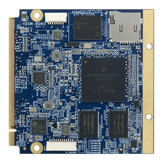
Carrier Board Design Guide for VIA QSM-8Q60 3. Qseven Specification Overview The carrier board for VIA QSM-8Q60 module must follow the placement defined in the Qseven specification. 3.1. Qseven Module Placement Figure 10 shows a depiction of the top view of 3.5” SBC form factor carrier board PCB with appropriate amount of space reserved for the Qseven module (VIA QSM-8Q60). -
Page 16: Via Qsm-8Q60 Module And Carrier Board Dimensions
Carrier Board Design Guide for VIA QSM-8Q60 3.3. VIA QSM-8Q60 Module and Carrier Board Dimensions The mechanical dimensions of the QSM-Q860module and reference carrier board (QSMDB2) are shown below. 70mm 5.1mm 2.69mm 3.95mm 52mm 70mm 62.11mm 54.53mm 18mm 2.5mm 64.9mm 70mm Figure 13: Dimensions of the VIA QSM-8Q60 module (top view) 137.19mm... -
Page 17: Mxm Connector
Carrier Board Design Guide for VIA QSM-8Q60 3.4. MXM Connector The MXM connector can handle high-speed signals and comprises of 230-pins to connect the VIA QSM- 8Q60 module. Table 5 shows the specification of MXM connector with 7.8mm height. Resulting height between Part Number Height Vendor... -
Page 18: Mxm Connector Footprint
Carrier Board Design Guide for VIA QSM-8Q60 3.4.2. MXM Connector Footprint 68.12mm 61.5mm Pin no. 230 0.61mm 51mm Pin no. 2 3.5mm 5.5mm 0.30mm 3mm (2X) 2.0mm 2.5mm 0.98mm 5.15mm (2X) 1.1mm 1.6mm 5.5mm 0.5mm Pin no. 1 Pin no. 229 (Pitch) 3.5mm 0.36mm... -
Page 19: Mxm Connector Pinouts
Carrier Board Design Guide for VIA QSM-8Q60 3.5. MXM Connector Pinouts The MXM connector is used for connecting the VIA QSM-8Q60 module to the Qseven carrier board. The MXM connector is consists of 230-pins. The pinout of the MXM connector is shown below. Pin# Pin Name Signal... - Page 20 Carrier Board Design Guide for VIA QSM-8Q60 USB_P5- USB_P4-/USB_SSRX1- USBD_T4- /USB_SSTX1- USB_P5- USB_P4-/USB_SSRX1+ USBD_T4+ /USB_SSTX1+ USB_2_3_OC# USB_2_3_OC USB_0_1_OC# USB_0_OTG_OC USB_P3- USBD_T3- USB_P2- USBD_T2- USB_P3+ USBD_T3+ USB_P2+ USBD_T2+ USB_CC USB_ID USBD_OTG_ID USB_P1- OTG_USBD_T1- USB_P0- USBD_T0- USB_P1+ OTG_USBD_T1+ USB_P0+ USBD_T0+ eDP0_TX0+ LVDS0_TX0_P eDP1_TX0+ LVDS1_TX0_P /LVDS_A0+...
-
Page 21: Table 6: Mxm Connector Pinout
Carrier Board Design Guide for VIA QSM-8Q60 DP_LANE0+ HDMI_D2P HDMI_CTRL_DAT I2C2_SDA /TMDS_LANE2+ DP_LANE0- HDMI_D2M HDMI_CTRL_CLK I2C2_SCL /TMDS_LANE2- DP_HDMI_HPD# HDMI_HPD RSVD PCIE_CLK_REF+ PCIe_CREFCLKP PCIE_WAKE# PCIE_WAKE_B PCIE_CLK_REF- PCIe_CREFCLKM PCIE_RST# PCIE_RST_B PCIE3_TX+ PCIE3_RX+ PCIE3_TX- PCIE3_RX- PCIE2_TX+ PCIE2_RX+ PCIE2_TX- PCIE2_RX- UART0_TX UART1_TX UART_RTS- UART1_-RTS PCIE1_TX+ PCIE1_RX+ CAN_TX2... -
Page 22: Figure 19: Mxm Connector Schematics
Carrier Board Design Guide for VIA QSM-8Q60 Figure 19: MXM connector schematics... -
Page 23: Layout And Routing Recommendations
Carrier Board Design Guide for VIA QSM-8Q60 4. Layout and Routing Recommendations The information presented in this chapter includes the signal descriptions, reference schematic examples, topology examples, and detailed layout and routing guidelines for each bus interface. The information provided is intended for designing the Qseven compliant carrier boards to support the features of VIA QSM-8Q60 module. -
Page 24: Figure 20: Minipcie Card And Slot Diagram
Carrier Board Design Guide for VIA QSM-8Q60 Ground No Connection/Reserved No Connection/Reserved Ground PCIE_RST_B PCI Express reset PCIe_CRXM Receiver differential pair negative signal, Lane 0 MPCIE_3V3 Auxiliary voltage source, 3.3V PCIe_CRXP Receiver differential pair positive signal, Lane 0 Ground Ground DDR_1_5V Secondary source voltage, 1.5V Ground... -
Page 25: Pci Express Layout And Routing Recommendations
Carrier Board Design Guide for VIA QSM-8Q60 The PCI Express signal has a point-to-point topology. The figure below shows the PCI Express x1 point- to-point bus connection from MXM connector to MiniPCI Express slot/device. Qseven Carrier Board MiniPCI Express slot/device MXM Connector (1-Lane) 0 ohm... -
Page 26: Pci Express Reference Schematics
Carrier Board Design Guide for VIA QSM-8Q60 Routing, layout, and trace properties for implementing PCI Express interface in the carrier board are listed in the following tables. AC Coupling Routing Signal Group Signal Name Signal Type Capacitors Topology PCIE0_TX+ None Transmit Paired Differential PCIE0_TX-... -
Page 27: Ethernet Interface
Carrier Board Design Guide for VIA QSM-8Q60 4.2. Ethernet Interface The VIA QSM-8Q60 module provides one Gigabit Ethernet (LAN) port that complies with the IEEE standard for 10BASE-T, 100BASE-T, 1000BASE-T, TX and T4 Ethernet interfaces. The Gigabit Ethernet (LAN) interface of the VIA QSM-8Q60 module consists of four differential signals and control signals for activity link indicators. -
Page 28: Ethernet Interface Topology
Carrier Board Design Guide for VIA QSM-8Q60 4.2.1. Ethernet Interface Topology This section shows the layout recommendations of both transmit and receive differential data pairs and single-ended control signal between the VIA QSM-8Q60 module and RJ-45 port with integrated magnetic module. -
Page 29: Gigabit Ethernet Layout And Routing Recommendations
Carrier Board Design Guide for VIA QSM-8Q60 4.2.2. Gigabit Ethernet Layout and Routing Recommendations • Route differential pairs close together and away from other signals. • Route any other trace parallel to one of the differential trace. • Keep trace length within each differential pair equal. •... -
Page 30: Gigabit Ethernet Reference Schematics
Carrier Board Design Guide for VIA QSM-8Q60 Trace & Spacing (mil) Pair to Pair Spacing to Signal Name Trace Impedance (S : W : S1 : W : S) Length Mismatch Other Group GBE_MDI0+ GBE_MDI0- GBE_MDI1+ GBE_MDI1- 100Ω ± 15% 20 : 5 : 8 : 5 : 20 5 mils 20 mils... -
Page 31: Usb Interface
Carrier Board Design Guide for VIA QSM-8Q60 4.3. USB Interface The Universal Serial Bus (USB) provides a bi-directional, isochronous, hot-attachable Plug and Play serial interface for adding external peripheral devices (e.g., game controllers, communication devices, and input devices) on a single bus. The USB interface of the VIA QSM-8Q60 module is compliant to USB 2.0 specification. -
Page 32: Figure 27: Usb Differential Signal Routing Example
Carrier Board Design Guide for VIA QSM-8Q60 Qseven Carrier Board Recommended USB port QSM-8Q60 Not recommended Connector Module USB port Figure 27: USB differential signal routing example Figure 28: USB 2.0 trace spacing diagram Routing, layout, and trace properties for implementing USB interface in the carrier board are listed in the following tables. -
Page 33: Table 18: Usb Interface Layout Guidelines
Carrier Board Design Guide for VIA QSM-8Q60 Accumulated Termination Signal Group Signal Name Routing Layer Note Stub Length Trace Length USB_P0+ Port 0 USB_P0- USB_P1+ Port 1 USB_P1- USB_P2+ Differential Port 2 Top or Bottom < 1″ < 4″ Data Pair USB_P2- USB_P3+ Port 3... -
Page 34: Usb Reference Schematics
Carrier Board Design Guide for VIA QSM-8Q60 4.3.2. USB Reference Schematics Figure 29: USB host reference circuitry The USB port mode can be controlled by the signal USB_ID. In the reference circuitry example below, the USB_ID signal is referenced to ground that makes the USB port 1 mode as Client USB (or USB OTG port). Figure 30: USB client reference circuitry... -
Page 35: Lvds Interface
Carrier Board Design Guide for VIA QSM-8Q60 4.4. LVDS Interface The LVDS interface in the VIA QSM-8Q60 module enables displaying graphics on LVDS flat panel. The LVDS is a dual-channel that supports 18-bit and 24-bit interfaces. The LVDS signal interface consists of four differential data pairs and one differential clock pair for each channel, and five single-ended control signals. -
Page 36: Lvds Layout And Routing Recommendations
Carrier Board Design Guide for VIA QSM-8Q60 Qseven Carrier Board MXM Connector 0 ohm LVDS0_TX[3:0]P LVDS_A[3:0]+ LVDS0_TX[3:0]N LVDS_A[3:0]- LVDS1_CLK_P/N LVDS_A_CLK+/- LVDS LCD Pane LVDS1_TX[3:0]P Connector LVDS_B[3:0]+ LVDS1_TX[3:0]N LVDS_B[3:0]- LVDS_B_CLK+/- LVDS0_CLK_P/N QSM-8Q60 Module LVDS_BLEN LVDS_BLEN Backlight Inverter LVDS_PWM2 LVDS_BLT_CTRL control connector Backlight and Power Power LVDS_PPEN... -
Page 37: Table 22: Lvds Interface Layout Guidelines
Carrier Board Design Guide for VIA QSM-8Q60 Accumulated Signal Group Signal Name Routing Layer Note Trace Length LVDS_A[3:0]+ LVDS_A[3:0]- Route each pair of Data Top or Bottom <1.8″ wires in parallel LVDS_B[3:0]+ LVDS_B[3:0]- LVDS_A_CLK+ LVDS_A_CLK- Route each pair of Clock Top or Bottom <1.8″... -
Page 38: Lvds Reference Schematics
Carrier Board Design Guide for VIA QSM-8Q60 4.4.2. LVDS Reference Schematics The following reference circuitry is an example of how to implement the LVDS interface on the carrier board. PDD_ 2A= 80m i l s LVDS1 LVDS1 LVDS0_TX0_N LVDS0_TX0_NC LVDS0_TX0_N LVDS0_TX0_P LVDS0_TX0_PC LVDS0_TX0_P... -
Page 39: Hdmi Interface
Carrier Board Design Guide for VIA QSM-8Q60 4.5. HDMI Interface The VIA QSM-8Q60 supports one HDMI interface. The HDMI is used to connect high definition video and digital audio using a single cable. It allows connecting the digital video devices to utilize a high definition video signal. -
Page 40: Hdmi Layout And Routing Recommendations
Carrier Board Design Guide for VIA QSM-8Q60 4.5.1. HDMI Layout and Routing Recommendations • Differential pair should be all referenced to ground. • Each trace of differential pairs should not have more than two via holes. • Each differential pairs signal should route to parallel to each other with the same trace length. •... -
Page 41: Hdmi Reference Schematics
Carrier Board Design Guide for VIA QSM-8Q60 4.5.2. HDMI Reference Schematics For HDM I ; c l os e t o TM DS141 3P3V DP1TX0+ C191 0.1uF/X C191 0.1uF/X C156 C156 C157 C157 C158 C158 C159 C159 C160 C160 C161 C161 C162 C162... -
Page 42: Audio Interface
Carrier Board Design Guide for VIA QSM-8Q60 4.6. Audio Interface The Audio interface is a link between the VIA QSM-8Q60 module and Audio Codec that supports the I bus in the carrier board. This section contains I S layout and routing information. The corresponding audio interface signals are defined in the table below. -
Page 43: Audio Reference Schematics
Carrier Board Design Guide for VIA QSM-8Q60 Signal Name Routing Layer Accumulated Trace Length Note HDA_RST#/I2S_RST# Top or Bottom HDA_SYNC/I2S_WS Route traces as HDA_BITCLK/I2S_CLK Top or Bottom short as possible HDA_SDO/I2S_SDO Top or Bottom HDA_SDI/I2S_SDI Table 30: Audio interface layout guidelines Trace Width Spacing to Signal Name... - Page 44 Taiwan Headquarters Japan China 1F, 531 Zhong-zheng Road, 940 Mission Court 3-15-7 Ebisu MT Bldg. 6F, Tsinghua Science Park Bldg. 7 Xindian Dist., New Taipei City 231 Fremont, CA 94539, Higashi, Shibuya-ku No. 1 Zongguancun East Road, Taiwan Tokyo 150-0011 Haidian Dist., Beijing, 100084 Japan China...
Need help?
Do you have a question about the Qseven QSM-8Q60 and is the answer not in the manual?
Questions and answers