Table of Contents
Advertisement
Quick Links
Trion
T8 BGA81
®
Development Kit User
Guide
T8F81C-DK-UG-v2.0
August 2020
www.efinixinc.com
Copyright
2020. All rights reserved. Efinix, the Efinix logo, Quantum, Trion, and Efinity are trademarks of Efinix, Inc. All other trademarks and
©
service marks are the property of their respective owners. All specifications subject to change without notice.
Advertisement
Table of Contents

Related Manuals for Efinix Trion T8 BGA81

Summary of Contents for Efinix Trion T8 BGA81
- Page 1 Copyright 2020. All rights reserved. Efinix, the Efinix logo, Quantum, Trion, and Efinity are trademarks of Efinix, Inc. All other trademarks and © service marks are the property of their respective owners. All specifications subject to change without notice.
-
Page 2: Table Of Contents
Contents Introduction............................. 3 What's in the Box?............................ 3 Register Your Kit............................3 Download the Efinity Software......................3 ® Installing Standoffs..........................3 Board Functional Description......................4 Features...............................4 Overview..............................5 Power On..............................6 Reset................................6 Clock Sources............................6 Headers............................... 7 User Outputs............................10 User Inputs............................... 10 Running the Demonstration Design..................... -
Page 3: Introduction
Trion T8 BGA81 Development Kit User Guide Introduction Thank you for choosing the Trion T8 BGA81 Development Kit (part number: ® T8F81C-DK), which allows you to explore the features of the T8 FPGA. Warning: Use correct anti-static methods when handling the board. -
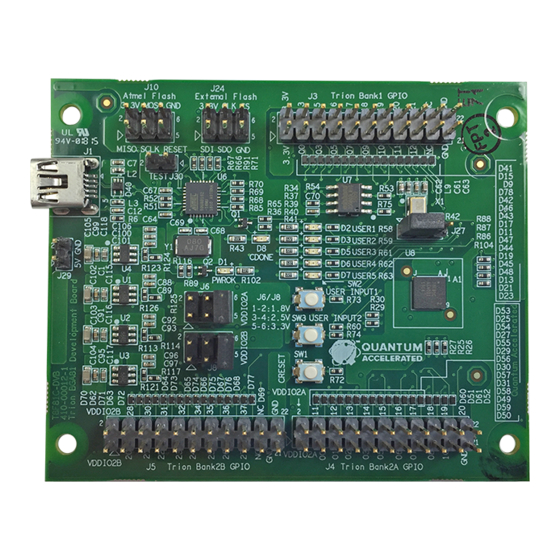
Page 4: Board Functional Description
Trion T8 BGA81 Development Kit User Guide Board Functional Description The Trion T8 BGA81 Development Board contains a variety of components to help you ® build designs for the Trion T8 device. ® Figure 1: Trion T8 BGA81 Development Board Block Diagram ®... -
Page 5: Overview
Trion T8 BGA81 Development Kit User Guide Overview The board features the Efinix T8 programmable device in a 81-ball FBGA package, which is ® fabricated using Efinix Quantum technology. The Quantum -accelerated programmable ® ™ ™ logic and routing fabric is wrapped with an I/O interface in a small footprint package. T8 devices also include embedded memory blocks and multiplier blocks (or DSP blocks). -
Page 6: Power On
Trion T8 BGA81 Development Kit User Guide Power On Upon power-up, the USB power supply is input to the on-board regulators to generate the required 3.3 V, 2.5 V, 1.8 V, and 1.1 V for components on the board. When these voltages are up and stable, the board asserts a “power good”... -
Page 7: Headers
Trion T8 BGA81 Development Kit User Guide Headers The board contains a variety of headers to provide power, inputs, and outputs, and to communicate with external devices or boards. Table 1: Trion T8 BGA81 Development Board Headers ® Reference Designator... - Page 8 Trion T8 BGA81 Development Kit User Guide Pin Number GPIOL_05 GPIOR_02 GPIOR_22 GPIOL_15 GPIOR_13 GPIOR_31 GPIOL_07 GPIOR_03 GPIOR_23 GPIOL_16 GPIOR_14 GPIOR_32 GPIOL_09 GPIOR_05 GPIOR_24 GPIOL_17 GPIOR_15 GPIOR_34 GPIOL_10 GPIOR_06 GPIOR_25 GPIOL_18 GPIOR_16 GPIOR_35 GPIOL_11 GPIOR_07 GPIOR_26 GPIOL_19 GPIOR_17 GPIOR_36 GPIOL_12...
- Page 9 Trion T8 BGA81 Development Kit User Guide Table 4: Header J6 Pin Assignments Pin Number Signal 1.8 V VDDIO2B 2.5 V VDDIO2B 3.3 V VDDIO2B • A shunt connecting J8 pins 1 and 2 selects 1.8 V. • A shunt connecting J8 pins 3 and 4 selects 2.5 V.
-
Page 10: User Outputs
Trion T8 BGA81 Development Kit User Guide User Outputs The board has 5 green user LEDs that are connected to I/O pins in T8F81C banks 1A/1B. By default, the T8F81C I/O connected to these LEDs have a pull-up resistor that turns the LEDs off;... -
Page 11: Creating Your Own Design
Trion T8 BGA81 Development Kit User Guide Creating Your Own Design The Trion T8 BGA81 Development Board allows you to create and explore designs for the ® T8 device. Efinix provides example code and designs to help you get started: ®...
Need help?
Do you have a question about the Trion T8 BGA81 and is the answer not in the manual?
Questions and answers