Panasonic SDR-S7P Service Manual
Sd video camera
Hide thumbs
Also See for SDR-S7P:
- Operating instructions manual (116 pages) ,
- Operating instructions manual (114 pages) ,
- Service manual (54 pages)
Table of Contents
Advertisement
Quick Links
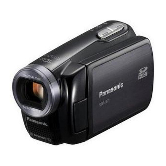
SDR-S7P
Model No.
SDR-S7PC
SDR-S7PL
SDR-S7PR
SDR-S7E
SDR-S7EB
SDR-S7EE
SDR-S7EF
SDR-S7EG
SDR-S7EP
SDR-S7GC
SDR-S7GD
SDR-S7GJ
SDR-S7GK
SDR-S7GN
SDR-S7GT
Vol. 2
Colour
(S)...........Silver Type (except PR,GD,GT)
(K)...........Black Type
© 2008 Matsushita Electric Industrial Co., Ltd. All
rights reserved. Unauthorized copying and distribu-
tion is a violation of law.
ORDER NO. VM0803026CE
SD Video Camera
B27
Advertisement
Chapters
Table of Contents

Subscribe to Our Youtube Channel
Related Manuals for Panasonic SDR-S7P


Summary of Contents for Panasonic SDR-S7P
- Page 1 ORDER NO. VM0803026CE SD Video Camera SDR-S7P Model No. SDR-S7PC SDR-S7PL SDR-S7PR SDR-S7E SDR-S7EB SDR-S7EE SDR-S7EF SDR-S7EG SDR-S7EP SDR-S7GC SDR-S7GD SDR-S7GJ SDR-S7GK SDR-S7GN SDR-S7GT Vol. 2 Colour (S)...Silver Type (except PR,GD,GT) (K)...Black Type © 2008 Matsushita Electric Industrial Co., Ltd. All rights reserved.
-
Page 2: Table Of Contents
TABLE OF CONTENTS PAGE PAGE 1 Safety Precaution -------------------------------------------------3 1.1. General Guidelines ----------------------------------------3 1.2. Leakage Current Cold Check ---------------------------3 1.3. Leakage Current Hot Check (See Figure 1.)--------3 2 Warning --------------------------------------------------------------4 2.1. Prevention of Electrostatic Discharge (ESD) to Electrostatically Sensitive (ES) Devices ----------4 2.2. -
Page 3: Safety Precaution
1 Safety Precaution 1.1. General Guidelines 1.3. Leakage Current Hot Check 1. IMPORTANT SAFETY NOTICE (See Figure 1.) There are special components used in this equipment 1. Plug the AC cord directly into the AC outlet. Do not use which are important for safety. These parts are marked by an isolation transformer for this check. -
Page 4: Warning
2 Warning 2.1. Prevention of Electrostatic Discharge (ESD) to Electrostatically Sensitive (ES) Devices Some semiconductor (solid state) devices can be damaged easily by static electricity. Such components commonly are called Elec- trostatically Sensitive (ES) Devices. Examples of typical ES devices are integrated circuits and some field-effect transistors and semiconductor "chip"... -
Page 5: Caution For Ac Cord(For Eb/Gc
2.3.2.3. How to Replace the Fuse A replacement fuse cover can be purchased from your local Panasonic Dealer. 1. Remove the Fuse Cover with a screwdriver. If the fitted moulded plug is unsuitable for the socket outlet in your home then the fuse should be removed and the plug cut off and disposed of safety. -
Page 6: How To Replace The Lithium Battery
2.4. How to Replace the Lithium Battery 2.4.1. Replacement Procedure 1. Remove the SIDE-R PCB. (Refer to Disassembly Procedures.) 2. Remove the Lithium battery (Ref. No. “B2501” at foil side of SIDE-R PCB) and then replace it into new one. NOTE: This Lithium battery is a critical component. -
Page 7: Service Navigation
3 Service Navigation 3.1. Introduction This service manual contains technical information, which allow service personnel’s to understand and service this model. Please place orders using the parts list and not the drawing reference numbers. If the circuit is changed or modified, the information will be followed by service manual to be controlled with original service manual. 3.2. -
Page 8: How To Define The Model Suffix (Ntsc Or Pal Model)
3.3. How to Define the Model Suffix (NTSC or PAL model) There are six kinds of SDR-S7. • a) SDR-S7P • b) SDR-S7PC • c) SDR-S7E/EB/EF/EG/EP • d) SDR-S7EE • e) SDR-S7GN • f) SDR-S7GK • g) SDR-S7GT • h) SDR-S7GD •... -
Page 9: Specifications
4 Specifications For P/PC/PL areas For other areas... -
Page 11: Service Fixture & Tools
5 Service Fixture & Tools 5.1. When Replacing the Main PCB After replacing the MAIN PCB, be sure to achieve adjustment. The adjustment instruction is available at “software download” on the “Support Information from NWBG/VDBG-PAVC” web-site in “TSN system”, together with Maintenance software. 5.2. - Page 12 3.The voltage being indicated on the schematic diagram is measured in "Standard-Playback" mode when there is no specify mode is mentioned. Model No. SDR-S7P SDR-S7EP 4.Although the voltage and waveform available on here is measured with standard frame, it may be differ from actual measurement due to modification of circuit and so on.
-
Page 13: S2. Voltage Chart
S2. Voltage Chart Note) Indicated voltage values are the standard values for the unit measured by the DC electronic circuit tester (high-impedance) with the chassis taken as standard. Therefore, there may exist some errors in the voltage values, depending on the internal impedance of the DC circuit tester. S2.1. -
Page 14: S3. Block Diagram
S3. Block Diagram S3.1. System Control Block Diagram IC6001 PW CPU VDD (SYSTEM CONTROL) IC6004 JK6901 TELE HI (A/V OUT) (EEPROM/32K-bit) REGD3V (2.9V) CL2501 CL2502 REMOCON PJ3/TCOIN REGD3V CL6039 TELE LOW CL6038 (1.93V) CL2503 CL2504 PG1/RXD1 CL6034 P70/ANA0 WIDE LOW PG0/TXD2 Q6501 (0.97V) -
Page 15: S3.2. Video/Audio Signal Process Block Diagram
S3.2. Video/Audio Signal Process Block Diagram IC3401 (SDRAM/512M-bit) IC601 (LCD CONTROLLER) 512MBit BANK0 BANK2 (4Mx32bitx4pcs) CKV1 STV1 BANK1 BANK3 COLUMN DECODER DECODER Y DECODERS I/O BUFFER & GATE ADDRESS BUFFER & REGISTER TIMING & MODE REGISTER PCG1 CKH2 DATA ADDRESS CTL SIG CLKIN CKH1... -
Page 16: S3.3. Sensor Block Diagram
S3.3. Sensor Block Diagram IC291 (CCD IMAGE SENSOR) IC302 (TG/AFE) FP6931 PW CCD-6R5V FP6931 PW CCD12V Q291 ADC IN PW REGD3V VOUT 10bit USER FP6931 CCD IN To VIDEO LOGIC 10bit (BUS9 ADIN0~9) CLAMP SCAN SP1,SP2,ADCK MAS/SLV To SYSCON PW REGD3V (CG RST) FP6931 OBP,PBLK... -
Page 17: S3.4. Lens Drive Block Diagram
S3.4. Lens Drive Block Diagram IC6001 (SYSTEM CONTROL) QR6002 K4 P52/A2 FP6971 ZLED CONT P50/A0 ZENC P51/A1 FLED CONT FENC ZOOM ENC FOCUS ENC PD7/TB15OUT FILTER CL701 H19 P71/ANA1 IC701 (LENS DRIVE) REFI EXT1 P54/A4 REFO EXT2 P55/A5 FP6971 HOLEOUT- HOLEIN+ EIR+ W18 PD6/TB14OUT... -
Page 18: S3.5. Power Block Diagram
S3.5. Power Block Diagram PW NOREG CL1011 RL1211 PW REGA5V CL1501 PW AF5V RL1001 PW VB5V JK6902 IP6901 Q1412 PW LCDBL5V CL1502 JACK To SYSCON Q1413 (LCD BL ON H) CL1031 PW REGD3R2V CL1511 D1 D1 D2 D2 Q1521 PW SD3R2V IP1511 S1 G1 S2 G2 IC1001... -
Page 19: S4. Schematic Diagram
S4. Schematic Diagram S4.1. Power Schematic Diagram SDR-S7 Series Power Section (Main P.C.B. (1/12)) Schematic Diagram... - Page 20 SDR-S7 Series Power Section (Main P.C.B. (1/12)) Schematic Diagram...
- Page 21 SDR-S7 Series Power Section (Main P.C.B. (1/12)) Schematic Diagram S-10...
- Page 22 SDR-S7 Series Power Section (Main P.C.B. (1/12)) Schematic Diagram S-11...
-
Page 23: S4.2. Video Schematic Diagram
S4.2. Video Schematic Diagram SDR-S7 Series Video Section (Main P.C.B. (2/12)) Schematic Diagram S-12 S-12... - Page 24 SDR-S7 Series Video Section (Main P.C.B. (2/12)) Schematic Diagram S-13...
- Page 25 SDR-S7 Series Video Section (Main P.C.B. (2/12)) Schematic Diagram S-14...
- Page 26 SDR-S7 Series Video Section (Main P.C.B. (2/12)) Schematic Diagram S-15...
-
Page 27: S4.3. Sd Holder Schematic Diagram
S4.3. SD Holder Schematic Diagram SDR-S7 Series SD Holder Section (Main P.C.B. (3/12)) Schematic Diagram S-16... -
Page 28: S4.4. Avio Schematic Diagram
S4.4. AVIO Schematic Diagram SDR-S7 Series AVIO Section (Main P.C.B. (4/12)) Schematic Diagram S-17... -
Page 29: S4.5. Charge Schematic Diagram
S4.5. Charge Schematic Diagram SDR-S7 Series Charge Section (Main P.C.B. (5/12)) Schematic Diagram S-18... - Page 30 S-19...
-
Page 31: S4.6. Main Cn Schematic Diagram
S4.6. Main CN Schematic Diagram SDR-S7 Series Main CN Section (Main P.C.B. (6/12)) Schematic Diagram S-20 S-20... - Page 32 SDR-S7 Series Main CN Section (Main P.C.B. (6/12)) Schematic Diagram S-21 S-21...
- Page 33 SDR-S7 Series Main CN Section (Main P.C.B. (6/12)) Schematic Diagram S-22...
- Page 34 SDR-S7 Series Main CN Section (Main P.C.B. (6/12)) Schematic Diagram S-23...
-
Page 35: S4.7. Tg Afe Schematic Diagram
S4.7. TG AFE Schematic Diagram SDR-S7 Series TG AFE Section (Main P.C.B. (7/12)) Schematic Diagram S-24... -
Page 36: S4.8. Lens Drive Schematic Diagram
S4.8. Lens Drive Schematic Diagram SDR-S7 Series Lens Driver Section (Main P.C.B. (8/12)) Schematic Diagram S-25... -
Page 37: S4.9. Syscon Schematic Diagram
S4.9. Syscon Schematic Diagram SDR-S7 Series Syscon Section (Main P.C.B. (9/12)) Schematic Diagram S-26... - Page 38 SDR-S7 Series Syscon Section (Main P.C.B. (9/12)) Schematic Diagram S-27 S-27...
- Page 39 SDR-S7 Series Syscon Section (Main P.C.B. (9/12)) Schematic Diagram S-28...
- Page 40 SDR-S7 Series Syscon Section (Main P.C.B. (9/12)) Schematic Diagram S-29...
-
Page 41: S4.10. Rtc Schematic Diagram
S4.10. RTC Schematic Diagram SDR-S7 Series RTC Section (Main P.C.B. (10/12)) Schematic Diagram S-30... -
Page 42: S4.11. Usb Host Schematic Diagram
S4.11. USB Host Schematic Diagram SDR-S7 Series USB Host Section (Main P.C.B. (11/12)) Schematic Diagram S-31... -
Page 43: S4.12. Mic Ir Schematic Diagram
S4.12. Mic IR Schematic Diagram SDR-S7 Series Mic IR Section (Main P.C.B. (12/12)) Schematic Diagram S-32... -
Page 44: S5. Print Circuit Board
S5. Print Circuit Board S5.1. Main P.C.B. S5.1.1. Main P.C.B. (Component Side) (Component Side) SDR-S7 Series Main P.C.B. (Component Side) S-33... -
Page 45: S5.1.2. Main P.c.b. (Foil Side
S5.1.2. Main P.C.B. (Foil Side) (Foil Side) SDR-S7 Series Main P.C.B. (Foil Side) S-34... -
Page 46: S5.1.3. Main P.c.b. Address Information
S5.1.3. Main P.C.B. Address Information Main P.C.B. Integrated Circuit QR3402 D1101 LB6906 C1014 C3306 C3474 C6030 R1042 R2001 R3492 R6045 IC301 QR3403 D1221 LB6907 C1015 C3308 C3475 C6031 R1043 R2301 R3496 R6048 IC302 QR3405 D1222 C1021 C3310 C3479 C6503 R1044 R2302 R3497 R6049... - Page 47 S-36...
-
Page 48: S6. Replacement Parts List
S6. Replacement Parts List Note: 1.* Be sure to make your orders of replacement parts according to this list. 2. IMPORTANT SAFETY NOTICE Components identified with the mark have the special characteristics for safety. When replacing any of these components, use only the same type. 3. - Page 49 SDR-S7P/PC/PL/PR/EG/E/EB/EF/EP/GC/GN/EE/GK/GJ/GT/GD vol.2 Ref.No. Part No. Part Name & Description Remarks Ref.No. Part No. Part Name & Description Remarks C1105 F1J0J106A049 C.CAPACITOR CH 6.3V 10U VEP03H52A MAIN P.C.B. 1 E.S.D. (RTL) P PC C1106 F1G0J1050007 C.CAPACITOR CH 6.3V 1U VEP03H52G MAIN P.C.B.
- Page 50 SDR-S7P/PC/PL/PR/EG/E/EB/EF/EP/GC/GN/EE/GK/GJ/GT/GD vol.2 Ref.No. Part No. Part Name & Description Remarks Ref.No. Part No. Part Name & Description Remarks C3440 F1G1C104A080 C.CAPACITOR CH 16V 0.1U C6031 F1H0J475A010 C.CAPACITOR CH 6.3V 4.7U C3441 F1G1C104A080 C.CAPACITOR CH 16V 0.1U C6503 F1G0J224A004 C.CAPACITOR CH 6.3V 0.22U...
- Page 51 SDR-S7P/PC/PL/PR/EG/E/EB/EF/EP/GC/GN/EE/GK/GJ/GT/GD vol.2 Ref.No. Part No. Part Name & Description Remarks Ref.No. Part No. Part Name & Description Remarks IP6901 K5H4021A0011 IC PROTECTOR QR1532 UNR32A400L TRANSISTOR-RESISTOR 1 E.S.D. QR1533 UNR32A400L TRANSISTOR-RESISTOR 1 E.S.D. JK6901 K2HZ110E0002 JACK QR2301 UNR31A300L TRANSISTOR-RESISTOR 1 E.S.D.
- Page 52 SDR-S7P/PC/PL/PR/EG/E/EB/EF/EP/GC/GN/EE/GK/GJ/GT/GD vol.2 Ref.No. Part No. Part Name & Description Remarks Ref.No. Part No. Part Name & Description Remarks R1211 D0YAR0000007 M.RESISTOR CH 1/16W R3418 ERJ2GEJ473Y M.RESISTOR CH 1/16W 47K R1251 D0YAR0000007 M.RESISTOR CH 1/16W R3419 ERJ2GEJ220 M.RESISTOR CH 1/16W 22...
- Page 53 SDR-S7P/PC/PL/PR/EG/E/EB/EF/EP/GC/GN/EE/GK/GJ/GT/GD vol.2 Ref.No. Part No. Part Name & Description Remarks Ref.No. Part No. Part Name & Description Remarks R4807 VRE0071E392 M.RESISTOR CH 1/10W 3.9K R4808 ERJ2GEJ124 M.RESISTOR CH 1/16W 120K X301 H0J360500014 CRYSTAL RESONATORS R4809 ERJ2GEJ333 M.RESISTOR CH 1/16W 33K...
Need help?
Do you have a question about the SDR-S7P and is the answer not in the manual?
Questions and answers