
Subscribe to Our Youtube Channel
Related Manuals for Sony KV-EF34N90


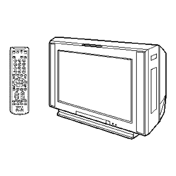
Summary of Contents for Sony KV-EF34N90
- Page 1 SERVICE MANUAL BG-3S CHASSIS MODEL COMMANDER DEST. CHASSIS NO. MODEL COMMANDER DEST. CHASSIS NO. KV-EF34N90 RM-913 TAIWAN SCC-P13EA TRINITRON COLOR TV ®...
- Page 2 CARBON PAINTED ON THE CRT, AFTER REMOVING THE PARTS LIST ARE CRITICAL TO SAFE OPERATION. REPLACE ANODE. THESE COMPONENTS WITH SONY PARTS WHOSE PART NUMBERS APPEAR AS SHOWN IN THIS MANUAL OR IN SUPPLEMENTS PUBLISHED BY SONY. – 2 –...
-
Page 3: Table Of Contents
KV-EF34N90 RM-913 TABLE OF CONTENTS Section Title Page Section Title Page SELF DIAGNOSIS FUNCTION 5. DIAGRAMS ........ 4 5-1. Block Diagram ............51 1. GENERAL ................ 8 5-2. Frame Schematic Diagram ........59 Circuit Boards Location .......... 63 2. DISASSEMBLY 5-4. -
Page 4: Self Diagnosis Function
KV-EF34N90 RM-913 SELF DIAGNOSTIC FUNCTION The units in this manual contain a self-diagnostic function. If an error occurs, the STANDBY/TIMER lamp will automatically begin to flash. The number of times the lamp flashes translates to a probable source of the problem. A definition of the STANDBY/TIMER lamp flash indicators is listed in the instruction manual for the user’s knowledge and reference. - Page 5 KV-EF34N90 RM-913 DISPLAY OF STANDBY/TIMER LIGHT FLASH COUNT Diagnostic Item Flash Count* +B overcurrent/overvoltage 2 times Vertical deflection stopped White balance failure 5 times * One flash count is not used for self-diagnostic. STOPPING THE STANDBY/TIMER FLASH Turn off the power switch on the TV main unit or unplug the power cord from the outlet to stop the STANDBY/TIMER lamp from flashing.
- Page 6 KV-EF34N90 RM-913 SELF-DIAGNOSTIC SCREEN DISPLAY For errors with symptoms such as “power sometimes shuts off” or “screen sometimes goes out” that cannot be confirmed, it is possible to bring up past occurances of failure for confirmation on the screen: [To Bring Up Screen Test] In standby mode, press buttons on the remote commander sequentially in rapid succession as shown below: [Screen display] / channel [5] / Sound volume [-] / Power ON...
- Page 7 KV-EF34N90 RM-913 SELF-DIAGNOSTIC CIRCUIT [+B overcurrent ªOCPº] Occurs when an overcurrent on the +B(135) line is detected by Q604 (A board). If Q604 (A board) go to ON and the voltage to pin 18 of IC301 (A board) should go down when V.SYNC is more than seven verticals in a period, the unit will automatically turn off.
-
Page 12: Set-Up Adjustments
KV-EF34N90 SECTION 3 RM-913 SET-UP ADJUSTMENTS • The following adjustments should be made when a complete Perform the adjustments in the following order : realignment is required or a new picture tube is installed. 1. Beam Landing • These adjustments should be performed with rated power 2. - Page 13 KV-EF34N90 RM-913 3-2. CONVERGENCE ADJUSTMENT V. STAT Preparation : • Before starting this adjustment, adjust the focus, horizontal size and vertical size. • Set the PICTURE and BRIGHTNESS 50%. • Cross hatch / Dot pattern. (1) Horizontal and Vertical Static Convergence H.
- Page 14 KV-EF34N90 RM-913 BMC (Hexapole) Magnet. (2) Dynamic Convergence Adjustment If the red, green and blue dots are not balanced or aligned, then Preparation: • use the BMC magnet to adjust in the manner described below. Before starting this adjustment, adjust the horizontal static convergence and the vertical static convergence •...
-
Page 15: Focus Adjustment
KV-EF34N90 RM-913 (3) Screen-corner Convergence 3-3. FOCUS ADJUSTMENT Note Focus adjustment should be completed before W/B adjustment. (1) Receive digital monoscope pattern. (2) Set "A/V CONTROL" to "STANDARD". a-d : screen-corner (3) Adjust FOCUS VR so that the center of the screen becomes misconvergence justfocus. -
Page 16: G2 (Screen) And White Balance Adjustments
KV-EF34N90 RM-913 4. SUB PICTURE BRIGHTNESS ADJUSTMENT 3-5. G2 (SCREEN) AND WHITE BALANCE 1) Set to service mode (Refer Section 4-1: ADJUSTMENTS WITH ADJUSTMENTS COMMANDER). 2) Input a PAL RF colorbar signal through Sub TUNER (TU3301). 1. G2 (SCREEN) ADJUSTMENT 3) BRIGHTNESS .. -
Page 17: Circuit Adjustments
KV-EF34N90 SECTION 4 RM-913 CIRCUIT ADJUSTMENTS 4-1. ADJUSTMENTS WITH COMMANDER Service adjustments are made with the RM-951 that comes with 1, 4 this unit. Select the adjustment item. ↓ a. ENTERING SERVICE MODE 3, 6 Raise/lower the data value. With the unit on standby ↓... -
Page 18: Adjustment Method
KV-EF34N90 RM-913 4-2. ADJUSTMENT METHOD Item Number 00 of device GEO Use the same method for all Items. Use 1 and 4 to select the This explanation uses H-Position as an example. 1. Select “GEO 00 HPS” with the 1 and 4 buttons. - Page 24 KV-EF34N90 RM-913 NOTE • shaded items are fixed data. • Standard data listed on the Adjustment Item Table are reference values, therefore it may be different for each model and for each mode. • Note for Different Data: Those are the standard data values written on the microprocessor. Therefore, the data values of the modes and stored respectively in the memory.
-
Page 25: Picture Quality Adjustments
KV-EF34N90 RM-913 4-3. PICTURE QUALITY ADJUSTMENTS SUB COLOR ADJUSTMENT (SCL) 1. Set to service mode. 110mV 2. Input RF PAL colorbar signal. Set A/V control to PERSONAL. 3. Set to VP7 (Service mode) "DYC" = 0 The highest level of VB1,VB2,VB4 4. -
Page 26: A Board Adjustment After Ic003 (Memory) Replacement
KV-EF34N90 RM-913 Y LEVEL (SUB PICTURE) ADJUSTMENT 4-4. A BOARD ADJUSTMENT AFTER IC003 (MEMORY) REPLACEMENT 1. Input a PAL colorbar signal. 2. Set to TWIN PICTURE mode. 3. Connect an oscilloscope to pin 2 (R-out) of CN705 on the C When replacing IC003 (MEMORY), be sure to change IC001 (µ-... -
Page 27: Picture Distortion Adjustment
KV-EF34N90 RM-913 4-5. PICTURE DISTORTION ADJUSTMENT (1) PICTURE DISTORTION ADJUSTMENT (2) Item Number 00 – 0B H-TRAPEZOID (Rotate RV1801) GEO 0 HPS (H POSITION) GEO 1 HSZ (H SIZE) GEO 2 PAP (PIN AMP) GEO 3 TLT (TRAPEZIUM) GEO 4... -
Page 28: Diagrams
KV-EF34N90 KV-EF34N90 KV-EF34N90 KV-EF34N90 SECTION 5 RM-913 RM-913 RM-913 RM-913 DIAGRAMS 5-1. BLOCK DIAGRAM IC3303 IC301 IC701 A/V SWITCH Y/C/J CN8300 CN8301 CN305 CN703 VIDEO AMP TU101 CN102 CN1307 CN1305 CN101 R,G,B V901 BUFFER BUFFER BUFFER DET OUT C OUT1... - Page 29 KV-EF34N90 KV-EF34N90 KV-EF34N90 KV-EF34N90 RM-913 RM-913 RM-913 RM-913 H1 (3/4)(FUNCTION SWITCH, REMOTE SENSOR) IC001 T 501 S1902 SYSTEM u-COM ENTER CN1905 CN904 CN201 CN1206 H DRIVE H OUT Q506 Q511 8 KEY2 KEY2 PROT 3 PROT2 PROT IC502 PIN CORR.
-
Page 30: Frame Schematic Diagram
KV-EF34N90 KV-EF34N90 KV-EF34N90 KV-EF34N90 RM-913 RM-913 RM-913 RM-913 5-2. FRAME SCHEMATIC DIAGRAM NS MUTE DEGAUSS CN3802 CN3803 N/S (B) CN510 CN1602 AC IN CN601 N/S (E) NECK ASSY AC OUT SP L OUT AC IN CN307 : S-MICRO N/S (E) -
Page 31: Schematic Diagrams And Printed Wiring Boards
KV-EF34N90 KV-EF34N90 KV-EF34N90 KV-EF34N90 RM-913 RM-913 RM-913 RM-913 MAIN TUNER, VIF, SIF, AV SW Y/C DECODE JUNGLE, PRINTED WIRING BOARD A BOARD POWER SUPPLY, DEFLECTION – A Board – D004 D614 D005 D615 IC001 B-10 D006 D616 IC002 D203 C-11... - Page 32 KV-EF34N90 KV-EF34N90 KV-EF34N90 KV-EF34N90 RM-913 RM-913 RM-913 RM-913 VIDEO SIGNAL PROCESSING, Y/C/J SWITCHER, PICTRE IMPROVEMENT, AUDIO AMP CONTROLLER [AC IN] PRINTED WIRING BOARDS – B Board – – F Board – • :Pattern from the side which enables seeing. •...
- Page 33 KV-EF34N90 KV-EF34N90 KV-EF34N90 KV-EF34N90 RM-913 RM-913 RM-913 RM-913 [MULTI IMAGE DRIVER] P BOARD IC9506 CXD2079Q – P Board – P BOARD WAVEFORMS Frame Memory P (2/3) BOARD WAVEFORMS 124~137 103~115 Memory Control C Bus Data Interpolation A-ch Clock Input 5.2Vp-p (V) 5.2Vp-p (V)
- Page 34 (7) Schematic Diagrams of P3/3, J and B Boards [COMPONENT, VIDEO IN] [RGB BUFFER] PRINTED WIRING BOARDS – J Board – – B Board – – – – – – – – –...
-
Page 35: Schematic Diagrams Of C And H1 Boards
(8) Schematic Diagrams of C and H Boards Schematic diagrams Schematic diagram ? P J 4 boards – – 1 board – – – – – –... - Page 36 KV-EF34N90 KV-EF34N90 KV-EF34N90 RM-913 RM-913 RM-913 [CONTROL S/W, INPUT TERMINAL ] [RGB OUT] – C Board – PRINTED WIRING BOARDS – H Board – C BOARD WAVEFORMS NTSC : 15.7Vp-p (H) PAL/SECAM : 135V NTSC : 13.6Vp-p (H) PAL/SECAM : 135Vp-p (H) NTSC : 15.0Vp-p (H)
-
Page 37: Schematic Diagrams Of Vm2 And Dh Boards
(9) Schematic Diagrams of VM and DH Boards – – – – – –... - Page 38 KV-EF34N90 RM-913 [VELOCITY MODULATION] [N/S COIL DRIVE] PRINTED WIRING BOARDS – VM Board – – DH Board – – 109 –...
- Page 39 KV-EF34N90 RM-913 ROTATION CIRCUIT, V-PIN CORRECTION PICTURE ROTATION CONTROL, V-PIN CONTROL PRINTED WIRING BOARD – D Board – BOARD WAVEFORMS 23.0Vp-p (V) – 110 –...
-
Page 40: Schematic Diagram Of D2 Board
KV-EF34N90 KV-EF34N90 RM-913 RM-913 (10) Schematic Diagram of D Board – 111 – – 112 –... -
Page 41: Semiconductors
KV-EF34N90 KV-EF34N90 RM-913 RM-913 5-5. SEMICONDUCTORS DIODE TRANSISTOR 5P6M AK04V0 MA111 DTA114EKA-T146 2SC3840(3) CXA1855S (48PIN) AU-01Z-V1 1SS355 DTC114EK CXA2130S (64PIN) LETTER SIDE D2L20U 2SA1037AK-T146-R CXP86332-008S (64PIN) EL1Z 2SA1162-G CXP750097-001S (52PIN) ERA22-08 2SC1623-L5L6 SAA5261 (52PIN) GP08D 2SC2712-YG STV5112 (15PIN) HSS83TD ANODE... - Page 42 KV-EF34N90 RM-913 SBX1981-11(12) S-80743AL-A7-S SBX3005-01 SE-135N MSM548331TS-K (100PIN) TOP VIEW TDA8172 PST9143NL (5PIN) LA6510 RU-1P MARKING SIDE VIEW – –...
-
Page 43: Exploded Views
KV-EF34N90 SECTION 6 RM-913 EXPLODED VIEWS NOTE: • • Items marked " ∗ " are not stocked since Items with no par t number and no The components identified by description are not stocked because they are seldom required for routine... -
Page 44: Chassis
KV-EF34N90 RM-913 6-2. CHASSIS : 7-685-648-71 SCREW +BVTP 3 × 12 : 7-685-663-71 SCREW +BVTP 4 × 16 REF. NO. PART NO. DESCRIPTION REMARK REF. NO. PART NO. DESCRIPTION REMARK ! 1-467-525-21 4-046-797-01 SCREW (3X12), (+)BVTAP CAP BLOCK, HIGH-VOLTAGE * A-1372-556-A H1 MOUNT... -
Page 45: Electrical Parts List
KV-EF34N90 SECTION 7 RM-913 The components identified by shading and mark ! are critical for safety. ELECTRICAL PARTS LIST Replace only with part number specified. REF. NO. PART NO. DESCRIPTION REMARK REF. NO. PART NO. DESCRIPTION REMARK NOTE: • Items marked " ∗ " are not stocked since they •... - Page 46 KV-EF34N90 RM-913 The components identified by shading and mark ! are critical for safety. Replace only with part number specified. REF. NO. PART NO. DESCRIPTION REMARK REF. NO. PART NO. DESCRIPTION REMARK C519 1-102-212-00 CERAMIC 820PF 500V C615 ! 1-119-886-51...
- Page 47 KV-EF34N90 RM-913 The components identified by shading and mark ! are critical for safety. Replace only with part number specified. REF. NO. PART NO. DESCRIPTION REMARK REF. NO. PART NO. DESCRIPTION REMARK CN602 * 1-508-786-00 PIN, CONNECTOR (5MM PITCH) 2P...
- Page 48 KV-EF34N90 RM-913 The components identified by shading and mark ! are critical for safety. Replace only with part number specified. REF. NO. PART NO. DESCRIPTION REMARK REF. NO. PART NO. DESCRIPTION REMARK <CHIP CONDUCTOR> <PHOTO COUPLER> JR002 1-216-295-91 SHORT PH600 ! 8-749-924-35...
- Page 49 KV-EF34N90 RM-913 The components identified by shading and mark ! are critical for safety. Replace only with part number specified. REF. NO. PART NO. DESCRIPTION REMARK REF. NO. PART NO. DESCRIPTION REMARK R016 1-216-025-91 RES,CHIP 1/10W R237 1-216-295-91 SHORT R017...
- Page 50 KV-EF34N90 RM-913 The components identified by shading and mark ! are critical for safety. Replace only with part number specified. REF. NO. PART NO. DESCRIPTION REMARK REF. NO. PART NO. DESCRIPTION REMARK R515 1-216-349-00 METAL OXIDE R585 1-249-381-11 CARBON 1/4W...
- Page 51 KV-EF34N90 RM-913 The components identified by shading and mark ! are critical for safety. Replace only with part number specified. REF. NO. PART NO. DESCRIPTION REMARK REF. NO. PART NO. DESCRIPTION REMARK R660 1-216-073-00 RES,CHIP 1/10W C1210 1-107-823-11 CERAMIC CHIP 0.47MF...
- Page 52 KV-EF34N90 RM-913 The components identified by shading and mark ! are critical for safety. Replace only with part number specified. REF. NO. PART NO. DESCRIPTION REMARK REF. NO. PART NO. DESCRIPTION REMARK C1279 1-164-690-91 CERAMIC CHIP 0.0022MF C3310 1-126-964-11 ELECT...
- Page 53 KV-EF34N90 RM-913 The components identified by shading and mark ! are critical for safety. Replace only with part number specified. REF. NO. PART NO. DESCRIPTION REMARK REF. NO. PART NO. DESCRIPTION REMARK C3375 1-126-964-11 ELECT 10MF C5315 1-163-243-11 CERAMIC CHIP...
- Page 54 KV-EF34N90 RM-913 The components identified by shading and mark ! are critical for safety. Replace only with part number specified. REF. NO. PART NO. DESCRIPTION REMARK REF. NO. PART NO. DESCRIPTION REMARK <FERRITE BEAD> <COIL> FB1205 1-410-397-21 FERRITE 1.1UH L1201...
- Page 55 KV-EF34N90 RM-913 The components identified by shading and mark ! are critical for safety. Replace only with part number specified. REF. NO. PART NO. DESCRIPTION REMARK REF. NO. PART NO. DESCRIPTION REMARK Q1320 8-729-230-49 TRANSISTOR 2SC2712-YG R1211 1-216-097-91 RES,CHIP 100K...
- Page 56 KV-EF34N90 RM-913 The components identified by shading and mark ! are critical for safety. Replace only with part number specified. REF. NO. PART NO. DESCRIPTION REMARK REF. NO. PART NO. DESCRIPTION REMARK R1316 1-216-025-91 RES,CHIP 1/10W R1379 1-216-089-91 RES,CHIP 1/10W...
- Page 57 KV-EF34N90 RM-913 The components identified by shading and mark ! are critical for safety. Replace only with part number specified. REF. NO. PART NO. DESCRIPTION REMARK REF. NO. PART NO. DESCRIPTION REMARK R3343 1-216-049-91 RES,CHIP 1/10W R5203 1-216-065-91 RES,CHIP 4.7K...
- Page 58 KV-EF34N90 RM-913 The components identified by shading and mark ! are critical for safety. Replace only with part number specified. REF. NO. PART NO. DESCRIPTION REMARK REF. NO. PART NO. DESCRIPTION REMARK R5334 1-216-081-00 RES,CHIP 1/10W <VARIABLE RESISTOR> R5335 1-216-081-00...
- Page 59 KV-EF34N90 RM-913 The components identified by shading and mark ! are critical for safety. Replace only with part number specified. REF. NO. PART NO. DESCRIPTION REMARK REF. NO. PART NO. DESCRIPTION REMARK R8306 1-216-025-91 RES,CHIP 1/10W D714 8-719-051-85 DIODE HSS83TD...
- Page 60 KV-EF34N90 RM-913 The components identified by shading and mark ! are critical for safety. Replace only with part number specified. REF. NO. PART NO. DESCRIPTION REMARK REF. NO. PART NO. DESCRIPTION REMARK R745 1-215-410-00 METAL 1/4W Q3809 8-729-119-78 TRANSISTOR 2SC2785-HFE...
- Page 61 KV-EF34N90 RM-913 The components identified by shading and mark ! are critical for safety. Replace only with part number specified. REF. NO. PART NO. DESCRIPTION REMARK REF. NO. PART NO. DESCRIPTION REMARK C2824 1-104-664-11 ELECT 47MF <TRANSISTOR> C2825 1-136-601-11 FILM 0.01MF...
- Page 62 KV-EF34N90 RM-913 The components identified by shading and mark ! are critical for safety. Replace only with part number specified. REF. NO. PART NO. DESCRIPTION REMARK REF. NO. PART NO. DESCRIPTION REMARK R2884 1-216-067-00 RES,CHIP 5.6K 1/10W * A-1372-556-A H1 MOUNT...
- Page 63 KV-EF34N90 RM-913 The components identified by shading and mark ! are critical for safety. Replace only with part number specified. REF. NO. PART NO. DESCRIPTION REMARK REF. NO. PART NO. DESCRIPTION REMARK <TRANSISTOR> <CONNECTOR> Q1901 8-729-030-02 TRANSISTOR DTC144ESA CN2410* 1-564-523-11...
- Page 64 KV-EF34N90 RM-913 The components identified by shading and mark ! are critical for safety. Replace only with part number specified. REF. NO. PART NO. DESCRIPTION REMARK REF. NO. PART NO. DESCRIPTION REMARK C9509 1-126-204-11 ELECT CHIP 47MF C9574 1-126-206-11 ELECT CHIP 100MF 6.3V...
- Page 65 KV-EF34N90 RM-913 The components identified by shading and mark ! are critical for safety. Replace only with part number specified. REF. NO. PART NO. DESCRIPTION REMARK REF. NO. PART NO. DESCRIPTION REMARK FL9504 1-233-504-21 FILTER, LOW PASS <TRANSISTOR> FL9505 1-233-504-21...
- Page 66 KV-EF34N90 RM-913 The components identified by shading and mark ! are critical for safety. Replace only with part number specified. REF. NO. PART NO. DESCRIPTION REMARK REF. NO. PART NO. DESCRIPTION REMARK R9433 1-216-065-91 RES,CHIP 4.7K 1/10W R9526 1-216-295-91 SHORT...
- Page 67 KV-EF34N90 RM-913 The components identified by shading and mark ! are critical for safety. Replace only with part number specified. P VM REF. NO. PART NO. DESCRIPTION REMARK REF. NO. PART NO. DESCRIPTION REMARK R9598 1-216-295-91 SHORT <CRYSTAL> R9599 1-216-295-91...
- Page 68 KV-EF34N90 RM-913 The components identified by shading and mark ! are critical for safety. Replace only with part number specified. REF. NO. PART NO. DESCRIPTION REMARK REF. NO. PART NO. DESCRIPTION REMARK Q5903 8-729-119-78 TRANSISTOR 2SC2785-HFE MISCELLANEOUS Q5904 8-729-119-76 TRANSISTOR 2SA1175-HFE...
- Page 69 Replace only with part number specified. REF. NO. PART NO. DESCRIPTION REMARK REF. NO. PART NO. DESCRIPTION REMARK Sony Corporation English 99GG70025-1 Sony TV Industries (M) Sdn. Bhd. Printed in Malaysia 9-965-748-01 TV Business of General Area 1999. 7 – 142 –...
Need help?
Do you have a question about the KV-EF34N90 and is the answer not in the manual?
Questions and answers