Table of Contents
Advertisement
SERVICE MANUAL
DVD SYSTEM
SYSTEM
HT-DV50
• This Service Manual is the "Revision Publishing" and replaces "Simple Manual"
AV-HD50 (EZ), (S/M Code No. 09-00C-439-7T1).
DVD
STEREO
PLAYER
RECEIVER
AV-HD50
XD-DV50
S/M Code No. 09-012-439-7R1
HT-DV50
BASIC DVD/CD MECHANISM : DV32BF
SPEAKER
SYSTEM
SX-AVW50
SX-CR677
EZ
REMOTE
CONTROLLER
RC-AAR05
RC-AVL01
Advertisement
Table of Contents

Related Manuals for Aiwa HT-DV50


Summary of Contents for Aiwa HT-DV50
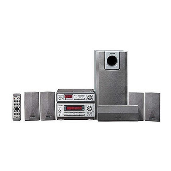
- Page 1 HT-DV50 SERVICE MANUAL DVD SYSTEM BASIC DVD/CD MECHANISM : DV32BF SPEAKER REMOTE STEREO SYSTEM PLAYER SYSTEM CONTROLLER RECEIVER SX-AVW50 RC-AAR05 HT-DV50 AV-HD50 XD-DV50 SX-CR677 RC-AVL01 • This Service Manual is the “Revision Publishing” and replaces “Simple Manual” AV-HD50 (EZ), (S/M Code No. 09-00C-439-7T1).
-
Page 2: Table Of Contents
TABLE OF CONTENTS SPECIFICATIONS ............................3 ~ 4 PROTECTION OF EYES FROM LASER BEAM DURING SERVICING ............5 MODEL NO. AV-HD50 ELECTRICAL MAIN PARTS LIST ......................6 ~ 11 TRANSISTOR ILLUSTRATION .......................... 12 WIRING – 1 (MAIN) <1 / 2> ..........................13 WIRING –... -
Page 3: Specifications
SPECIFICATIONS Stereo Receiver AV-HD50 Input/Output Input AUDIO VIDEO 1 IN, AUDIO VIDEO 2 FM tuner section IN : 360 mV (47 kohms) Tuning range 87.5 MHz to 108 MHz DIGITAL IN MD, DIGITAL IN DVD : Usable sensitivity (IHF) 16.2 dBf accept linear PCM signals and Dolby Antenna jack 75 ohms (unbalanced) - Page 4 DVD Player XD-DV50 Speaker System SX-AVW50 Speakers Front, Surround, Center : full range, Colour system DVD : PAL 70 mm cone type VCD : NTSC/PAL (Switchable) Subwoofer : 140 mm x 2, bass reflex Supported discs DVD video discs type 12 cm (single-sided single-layer, Impedance 3 ohms...
-
Page 5: Protection Of Eyes From Laser Beam During Servicing
PROTECTION OF EYES FROM LASER BEAM DURING SERVICING CAUTION This set employs laser. Therefore, be sure to follow carefully the instructions below when servicing. WARNING! ATTENTION ADVARSEL! This Compact Disc player is classified as a CLASS 1 LASER product. The CLASS 1 LASER PRODUCT label is located on the rear exterior. -
Page 6: Electrical Main Parts List
MODEL NO. AV-HD50 ELECTRICAL MAIN PARTS LIST REF. NO. PART NO. KANRI DESCRIPTION REF. NO. PART NO. KANRI DESCRIPTION 87-A40-574-080 ZENER,MTZJ3.0A 87-A40-269-080 C-DIODE,MC2836 87-A21-918-040 C-IC,NJM4558V 87-A40-270-080 C-DIODE,MC2838 87-A21-862-010 IC,STR-F6676 87-017-931-080 ZENER,MTZJ5.6B 87-A21-819-010 IC,SE013E 87-A40-002-080 ZENER,MTZJ5.1C 87-020-970-010 IC,NJM79L09 87-A20-389-010 IC,NJM7809FA 87-A40-956-080 DIODE,EK04 87-A40-553-080 DIODE,1N4003 LES... - Page 7 REF. NO. PART NO. KANRI DESCRIPTION REF. NO. PART NO. KANRI DESCRIPTION C109 87-010-805-080 CAP, S 1-16 C438 87-016-369-080 C-CAP,S 0.033-25 B K C110 87-010-805-080 CAP, S 1-16 C439 87-016-369-080 C-CAP,S 0.033-25 B K C111 87-010-805-080 CAP, S 1-16 C440 87-016-369-080 C-CAP,S 0.033-25 B K C112...
- Page 8 REF. NO. PART NO. KANRI DESCRIPTION REF. NO. PART NO. KANRI DESCRIPTION C116 87-010-322-080 C-CAP,S 100P-50 CH S116 87-A90-095-080 SW,TACT EVQ11G04M C117 87-010-322-080 C-CAP,S 100P-50 CH S117 87-A90-095-080 SW,TACT EVQ11G04M C118 87-010-322-080 C-CAP,S 100P-50 CH S118 87-A90-095-080 SW,TACT EVQ11G04M C120 87-010-322-080 C-CAP,S 100P-50 CH SW101...
- Page 9 REF. NO. PART NO. KANRI DESCRIPTION REF. NO. PART NO. KANRI DESCRIPTION C318 87-010-196-080 CHIP CAPACITOR,0.1-25 C625 87-012-154-080 C-CAP,S 150P-50 CH C319 87-010-248-080 CAP, ELECT 220-10V C626 87-012-154-080 C-CAP,S 150P-50 CH C320 87-010-196-080 CHIP CAPACITOR,0.1-25 C627 87-010-196-080 CHIP CAPACITOR,0.1-25 C321 87-A12-091-080 CAP,E 10-50 SMG C628...
- Page 10 REF. NO. PART NO. KANRI DESCRIPTION REF. NO. PART NO. KANRI DESCRIPTION C902 87-010-382-080 CAP, ELECT 22-25V C790 87-016-034-080 CHIP CAP U 0.027-25F C906 87-010-322-080 C-CAP,S 100P-50 CH C791 87-010-831-080 C-CAP,U,0.1-16F C907 87-010-196-080 CHIP CAPACITOR,0.1-25 C792 87-012-286-080 C-CAP,U 0.01-25 K B C908 87-010-374-080 CAP, ELECT 47-10V...
- Page 11 REF. NO. PART NO. KANRI DESCRIPTION REF. NO. PART NO. KANRI DESCRIPTION C982 87-010-831-080 C-CAP,U,0.1-16F D903 87-A41-048-040 C-VARI-CAP,HVM16-03 TL C983 87-A11-132-080 CAP,TC U 0.01-50 K B J832 87-A61-534-010 TERMINAL,ANT PAL AJ-2021 C984 87-012-286-080 C-CAP,U 0.01-25 K B J940 87-A60-633-010 CONN,2P H 2.5MM JMT C985 87-012-195-080 C-CAP,U 100P-50CH...
-
Page 12: Transistor Illustration
TRANSISTOR ILLUSTRATION E C B E C B E C B B C E 2SA1015 2SB1370 CSC2001 CSD1489 2SC2001 CSC4115 2SC1815 KTA1266 KTC3198 E C B 2SK2158 2SA1235 DTC123JK 2SK360 2SA1357 2SC3052 KRA107S 2SC2714 RT1N144C CMBT5401 RT1P141C CSD1306 – 12 –... -
Page 13: Wiring - 1 (Main) <1 / 2
WIRING – 1 (MAIN) <1 / 2> – 13 –... -
Page 14: Wiring - 1 (Main) <2 / 2
WIRING – 1 (MAIN) <2 / 2> – 14 –... -
Page 15: Schematic Diagram - 1 (Main)
SCHEMATIC DIAGRAM – 1 (MAIN) – 15 –... -
Page 16: Wiring - 2 (Front / Hp / Led) <1 / 2
WIRING – 2 (FRONT / HP / LED) <1 / 2> – 16 –... -
Page 17: Wiring - 2 (Front / Hp / Led) <2 / 2
WIRING – 2 (FRONT / HP / LED) <2 / 2> – 17 –... -
Page 18: Schematic Diagram - 2 (Front / Hp / Led)
SCHEMATIC DIAGRAM – 2 (FRONT) – 18 –... -
Page 19: Wiring - 3 (Func) <1 / 2
WIRING – 3 (FUNC) <1 / 2> – 19 –... -
Page 20: Wiring - 3 (Func) <2 / 2
WIRING – 3 (FUNC) <2 / 2> – 20 –... -
Page 21: Schematic Diagram - 3 (Func)
SCHEMATIC DIAGRAM – 3 (FUNC) – 21 –... -
Page 22: Wiring - 4 (Tuner)
WIRING – 4 (TUNER) – 22 –... -
Page 23: Schematic Diagram - 4 (Tuner)
SCHEMATIC DIAGRAM – 4 (TUNER) – 23 –... -
Page 24: Ic Block Diagram
IC BLOCK DIAGRAM – 24 –... - Page 25 – 25 –...
-
Page 26: Lcd Display
LCD DISPLAY SEGMENT WIRING COMMON WIRING – 26 –... -
Page 27: Ic Description
IC DESCRIPTION IC, UPD780308-033 Pin No. Pin Name Description I-STEREO Tuner stereo detection input. "L": stereo. I-TUNE/IFC Tuner TUNE/IFC detection input. O-CLK(M) Function IC, PLL, SW VOL clock output. O-DATA(M) Function IC, PLL, SW VOL data output. O-CLK-SHIFT Micro computer shift clock output. —... - Page 28 Pin No. Pin Name Description O-POWER System power on (Active "H"). I-PROTECT Protector input (Active "H"). O-RELAY-SW Relay output. O-LED LED input (Active "L"). O-SLEEP Sleep output (Active "L"). I-FAULT Fault input (Active "H"). O-SWF CTL Subwoofer control output. I-HP-MUTE Detect headphone plug insertion.
- Page 29 IC, YSS912 Pin No. Pin Name Description VDD1 +5V power supply for (I/Os). RAMCEN External SRAM interface / CE. (Not used) RAMA16 External SRAM interface address 16. (Not used) RAMA15 External SRAM interfce address 15. (Not used) 5~7,12 SDIB0~2, SDIB3 PCM input 0~3 to Sub DSP.
- Page 30 Pin No. Pin Name Description /SDBCK0 Inverted SDBCK0 clock output . (Not used) 58,59 RAMA6,5 External SRAM interface address 6, 5. (Not used) Ground. RAMA4 External SRAM interface address 4. (Not used) Initial clear. TEST Test terminal (Not used). RAMA3 External SRAM interface address 3.
- Page 31 IC, AK4112A Pin No. Pin Name Description DVDD Digital power supply pin, 3.3V. DVSS Digital ground pin. TVDD Input buffer power supply pin, 3.3V or 5V. DVD1OUT Transmit channel (through data) output pin in serial mode. Crystal input pin. Crystal output pin. (Not used) Power-down mode pin.
- Page 32 IC, M61501FP Pin No. Pin Name Description Not connected. ING R Right input selector G input. (Connected to GND) REC OUT R Right input B through output. Not connected. SEL OUT R Right signal after 0/-6 dB output. D OUT R Right tone A signal input.
- Page 33 Pin No. Pin Name Description SUR-L SL channel signal output. SLCH NIN SL channel B select signal input. SLCH DIN SL channel A select signal input. AGND SL channel analog GND. LCH BB1 L channel bass boost control input. LCH BB0 L channel bass boost control input.
- Page 34 IC, AK4527VQ Pin No. Pin Name Description SDTO source select pin. (Note 1) SDOS "L": Internal ADC output, "H": DAUX input. (Connected to DVSS) Control mode select pin. (Connected to DVSS) Soft mute pin. (Note 1) SMUTE When this pin goes to "H", soft mute cycle is initialized. When returning to "L", the output mute releases.
- Page 35 Pin No. Pin Name Description Common voltage output pin, AVDD/2. VCOM Large external capacitor around 2.2µF is used to reduce power-supply noise. VREFH Positive voltage reference input pin, AVDD. AVDD Analog power supply pin, 4.5 ~ 5.5V. AVSS Analog ground pin, 0V. Zero input detect 1 pin.
- Page 36 IC, TA2020-020 Pin No. Pin Name Description 1,5,15 Not connected. +5INA, +5INB Digital +5V, analog +5V. AGND1 Analog ground. Reference resistor. OVERLOAD A logic low output indicates the input signal has overloaded the amplifier. (Not used) AGND2 Analog ground. 9,12 VP1,VP2 Input stage feedback drive.
-
Page 37: Adjustment
ADJUSTMENT < TUNER SECTION > 1. Clock Frequency Check 6. FM Tracking Adjustment Settings : • Test point : TP2 (CLK) Settings : • Test point : TP8 (Rch), TP9 (Lch) Method : Set to AM 1602kHz and check that the test point is •... -
Page 38: Mechanical Exploded View 1 / 1
MECHANICAL EXPLODED VIEW 1 / 1 SH,LCD INSULATION CHAS,MAIN – 38 –... -
Page 39: Mechanical Parts List 1 / 1
KANRI DESCRIPTION 1 8A-AR6-004-010 PANEL,TOP 21 88-AR1-218-010 HLDR,PWB H8.9 2 8A-AR6-044-010 WINDOW,DISP EZ 22 8A-AR6-212-010 HLDR,PWB TU 3 8A-AV6-008-010 BADGE,AIWA 25 SIL 23 8A-AR6-214-010 HLDR,FAN 4 8A-AR6-010-010 KNOB,RTRY VOL 24 8Z-CL1-663-010 FAN,MF40D-12-200MM 5 8A-AR6-021-010 CABI,FR EZ 25 8A-AR6-011-010 FOOT,AAR 6 8A-AR6-019-010... -
Page 40: Electrical Main Parts List
MODEL NO. XD-DV50 ELECTRICAL MAIN PARTS LIST REF. NO. PART NO. KANRI DESCRIPTION REF. NO. PART NO. KANRI DESCRIPTION C0005 87-A11-976-080 C-CAP,E 470-16 M 10.5L MV C0006 87-A12-416-080 C-CAP,E 100U-25 M 7.7L UD 8Z-AV2-630-010 C-IC,L64021D C0007 87-016-669-080 C-CAP,S 0.1-25 K B 8Z-AV2-628-010 C-IC,HD6412350F20 C0008... - Page 41 REF. NO. PART NO. KANRI DESCRIPTION REF. NO. PART NO. KANRI DESCRIPTION C0222 87-010-831-080 C-CAP,U 0.1-16 Z F C0342 87-012-180-080 C-CAP,U 22P-50 J CH C0224 87-012-277-080 C-CAP,U 1800P-50 K B GRM C0343 87-012-270-080 C-CAP,U 470P-50 K B C0225 87-012-274-080 C-CAP,U 1000P-50 K B C0344 87-012-195-080 C-CAP,U 100P-50 J CH...
- Page 42 REF. NO. PART NO. KANRI DESCRIPTION REF. NO. PART NO. KANRI DESCRIPTION C0712 87-012-286-080 C-CAP,U 0.01-25 K B C0838 87-012-174-080 C-CAP,U 12P-50 J CH C0713 87-012-286-080 C-CAP,U 0.01-25 K B C0839 87-012-178-080 C-CAP,U 18P-50 J CH C0714 87-012-286-080 C-CAP,U 0.01-25 K B C0844 87-012-168-080 C-CAP,U 6P-50 D CH...
- Page 43 REF. NO. PART NO. KANRI DESCRIPTION REF. NO. PART NO. KANRI DESCRIPTION R0012 87-022-284-080 C-RES,U 68K-1/16W F LED0500 87-A41-095-010 LED,SELS5B20C ORG R0013 87-022-285-080 C-RES,U 82K-1/16W F LED0501 87-A41-095-010 LED,SELS5B20C ORG R0020 87-022-241-080 C-RES,U 12K-1/16W F S0500 87-A90-164-080 SW,TACT SKQNAB(N) R0021 87-022-223-080 C-RES,U 2.2K-1/16W F S0501...
-
Page 44: Transistor Illustration
TRANSISTOR ILLUSTRATION 3LN01C 2SA1037 2SB1132 FTS1002 2SA1586 2SC2412 2SC3326 2SC4116 2SC4213 DTA114EK DTA144EK DTC144EK DTC144EU – 44 –... -
Page 45: Block Diagram
BLOCK DIAGRAM PICK UP IC700 (MPEG Decoder) IC301 RF AMP L64021D OPTICAL OUT U001 IC201 DSP&SERVO LA9702W LC78660 18-24 33 34 SP_DIF CN300 DVD EQ DVD RF 40,41 BOOT3T Dolby Digital (A+B+C+D) Servo DVD_RF Decoder SDT0-7 CD EQ DEFECTI BCATH 12-19 DVD_A PreParser... -
Page 46: Wiring - 1 (Main) - Bottom View
WIRING - 2 (MAIN C.B) -Bottom View- COLOR SCHEMATIC DESCRIPTION TO FE PROGRAM WRITING IIG DC IN MICON VCC D/D OUT A 5V‑1 A 5V‑2 RF VCC D 5V‑3 D 5V‑2 D 5V‑5 REG.+3.3V D 8V VCC D 3V 2.5V 2.5V‑2 -46-... -
Page 47: Wiring - 1 (Main) - Top View
WIRING - 1 (MAIN C.B) -Top View- -47-... - Page 48 SCHEMATIC DIAGRAM - 1 (MAIN C.B -1/5) MICON VCC 1A TO MAIN C.B 4/5 (SYSCON SECTION) MAIN C.B 1/5 (POWER, VIDEO SECTION) TP023 TP015 A 5V‑1 TO MAIN C.B 5/5 (AV DECODER SECTION) TP021 RF VCC TO MAIN C.B 2/5 (SERVO, DSP SECTION) D 5V‑3 TO MAIN C.B 3/5 (RF AMP SECTION) TP001 TP004 TP008 TP017 TO MAIN C.B 2/5 D 5V‑2 (SERVO, DSP SECTION) TP010 TP002 TP025 D 5V‑5 TO MAIN C.B 5/5 (AV DECODER SECTION) REG.+3.3V 11A TO MAIN C.B 5/5 (AV DECODER SECTION) TP019 TO MAIN C.B 2/5...
- Page 49 SCHEMATIC DIAGRAM - 2 (MAIN C.B -2/5) MAIN C.B 2/5 (SERVO, DSP SECTION) TP218 TP200 D‑RAM I/F DVD Decoder RF I/F TP217 CLV/CAV EFM PLL TP208 TP212 Servo Frame sysc Protect Combine Frame sync TP213 EFM Detector Sub Code TP211 Audio TP210 TP209 CIRC Decoder CD‑ROM Decoder AV Decoder CPU I/F Clock Gen. Sys PLL TP136 TP101 TP137 TP138 TP139 TP132 TP131 TP140 TP130...
-
Page 50: Schematic Diagram - 10 (Front)
SCHEMATIC DIAGRAM - 3 (MAIN C.B -3/5) MAIN C.B 3/5 (RF AMP SECTION) TP309 TP314 TP313 TP316 DVD TE DVD,CD TE Generator CD TE TP318 Generator TP317 Reflect APC1 Amp. (DVD) APC1 (CD) LPF1 TP306 LPF2 TP304 TP308 TP319 TP320 TP305 TP307 TP303 TP327 TP302 D 5V‑3 2.5V 2.5V‑2 -50-... - Page 51 SCHEMATIC DIAGRAM - 4 (MAIN C.B -4/5) MAIN C.B 4/5 (SYSCON SECTION) TP616 TP615 TP610 3‑State Buff. Driver TP611 TP612 TP613 TP617 3‑State Buff. Driver Bus Transceiver TP605 TP604 TP603 TP607 -51-...
- Page 52 SCHEMATIC DIAGRAM - 5 (MAIN C.B -5/5) MAIN C.B 5/5 (AV DECODER SECTION) TP711 TP706 TP705 TP712 TP714 TP713 Memory Interface Audio Decoder Channel Decoder Interface Video Decoder Video D 5V‑5 Interface A 5V‑2 Host Interface REG.+3.3V TP707 TP708 -52-...
- Page 53 WIRING - 3 (FRONT C.B) SENSOR C. B DECK C. B PICK-UP SPINDLE MOTOR CNA402 CON1 PHOTO INTERRUPTER TO MAIN C.B FFC1 CN300 LIMIT SWITCH CON2 SLED MOTOR -53-...
- Page 54 SCHEMATIC DIAGRAM - 6 (FRONY C.B) FRONT C.B -54-...
-
Page 55: Lcd Display
LCD DISPLAY – 55 –... -
Page 56: Ic Block Diagram
IC BLOCK DIAGRAM IC, BA00ASFP IC, SN74LV541APW – 56 –... - Page 57 IC, NJM2267M IC, MM1454XFBE VIN2 6.2dB 75Ω VOUT2 DRIVER 750Ω VSAG2 2.2kΩ 2.07kΩ VIN1 6.2dB 75Ω VOUT1 DRIVER 750Ω VSAG1 2.2kΩ 2.07kΩ IC, LC75854W 39 38 37 36 35 34 33 32 31 30 29 28 27 26 25 24 23 22 21 20 19 18 17 16 15 14 13 12 SEGMENT DRIVER &...
- Page 58 IC, LA6556L-TE-L S-GND MUTE2 MUTE2 MUTE1 VCC2 MUTE1 LLD- VIN4 VLD+ VIN4- VO4+ VIN4+ VO4- VREF-IN VO3- VIN1(VREF)-SW VIN1/VREF-SW VO3+ VREF-OUT(CH1) REG-OUT VO2+ REG-IN VO2- VIN3+ VO1+ VIN3- VO1- VIN3 VCC1 VIN2+ VIN1 VIN1-A VIN2- AMP-A VIN2 VIN1+A VIN1(VREF)-SW VIN1-B VIN1+B L:AMP-A AMP-B...
- Page 59 IC, PCM1723 Internal System Clock Data ROM Counter N Phase Detector & Loop Filter Counter M MCKO SCKO 27 MHz 256 fs / 384 fs IC, S-8520B28MC REFERENCE POWER SUPPLY VOUT CONTROL CIRCUIT ON/OFF ON/OFF IC, SN74LV245APW – 59 –...
-
Page 60: Ic Description
IC DESCRIPTION IC, MC44722AVFU Pin No. Pin Name Description CVBS/CB Analog composite video signal or Cb signal output current drive (positive) CVBS/CB Analog composite video signal or Cb signal output current drive (negative) CVBS/CBVDD Power supply for CVBS/Cb DAC circuit Analog luminance signal output current drive (positive) Analog luminance signal output current drive (negative) YVDD... - Page 61 IC, L64021D Pin No. Pin Name Description Ground. 2 ~ 5 SBD_7 ~ 4 SDRAM data bus 7 ~ 4. Power (3.3V). 7 ~ 10 SBD_3 ~ 0 SDRAM data bus 3 ~ 0. Ground. 12 ~ 19 CH_DATA_0 ~ 7 Channel data bus 0 ~ 7.
- Page 62 Pin No. Pin Name Description Power (3.3V). OSD_ACTIVE On screen display active. 73, 74 PD_0, 1 Pixel data output bus 0, 1. Ground. 76-78 PD_2-4 Pixel data output bus 2-4. Power (3.3V). — Not connected. Ground. 82 ~ 84 PD_5 ~ 7 Pixel data output bus 5 ~ 7.
- Page 63 Pin No. Pin Name Description Ground. 124 ~ 126 SBD_12 ~ 10 SDRAM data bus 12 ~ 10. Power (3.3V). 128, 129 SBD_9, 8 SDRAM data bus 9, 8. SCLK SDRAM 81MHz clock. Ground. 132 ~ 134 SBA_9 ~ 7 SDRAM address bus 9 ~ 7.
- Page 64 IC, HD6412350F20 Pin No. Pin Name Description CS1ROM — Not used. CS0ROM Chip select output terminal for ROM. 3, 4 GND. Power input terminal. EVER 5 V. 6 ~ 9 A0 ~ 3 Address bus output terminal. GND. 11 ~ 18 A4 ~ 11 Address bus output terminal.
- Page 65 Pin No. Pin Name Description USDA C data input/output terminal for EEPROM, video encoder IC. Data enable signal output terminal for AUDIO DAC IC control. Clock for AUDIO DAC IC control. Data output terminal for AUDIO DAC IC control. WDTOVF Watch dog timer overflow signal output terminal.
- Page 66 Pin No. Pin Name Description AMUTE Audio signal (analog audio) output mute control terminal ON = H OFF = L. POWER ON Power supply control terminal ON = H OFF = L. A MUTE AC-3 — Not used. YS917 CS —...
- Page 67 IC, LC87F72C8A Pin No. Pin Name Description SUBRXD DATA input terminal for LOADER serial communication control. SUBSCK Clock input terminal for LOADER serial communication control. LEDD1 Detection of LEDD1. LEDCSB Detection of LEDCSB. LEDCLK Detection of LEDCLK. RDY_HIF LOADER READY signal output terminal. Detection of PWM.
- Page 68 Pin No. Pin Name Description CURRENT RF general-purpose port output pin 2. RW_DISC RW DISC control output pin. DUAL DUAL control output pin. DECRESB Decoder reset output pin. EVARESOB System reset output pin. 61 ~ 65 AB8-12 Address 8-12. 66-68 S37-39/PE5 ~ 7 Detection of S37-39/PE5 ~ 7.
- Page 69 IC, LC78660W Pin No. Pin Name Description RFPI RF input port pin. (Pull down) TEST0 Tracking margin signal I/O pin. DVDD2 — A/D D/A internai logic power supply. [Digital 5V] DVSS — Digital GND. AD5/BH Servo A/D input pin. (AD5: Assistant input 5) AD4/PH/TE Servo A/D input pin.
- Page 70 Pin No. Pin Name Description FG counter input pin. EVENT EVENT counter input pin. (Pull down) HFLIO Mirror detest signal I/O pins. 45 ~ 48 PP0 ~ 3 General-purpose port 0 ~ 3. (Pull down) Subcode Q read ready monitor pin. HFBUSYB DSP command dispose busy signal output pin.
- Page 71 Pin No. Pin Name Description Oscillator circuit input pin. XOUT Oscillator circuit outpit pin. DVDD6 — Oscillator circuit power supply. [Digital 3.3V] 109, 110 PP6, 7 General-purpose port6, 7. (Pull down) AVREQIO AV data demand flag I/O pins. AVACKOI AV data read strobe output pin. AVDACK AV data read (Clock/Enable) output pins.
- Page 72 Pin No. Pin Name Description AVSS — Analog GND. 159 ~ 166 MD15 ~ 8 DRAM data15 ~ 8. DVDD5 — I/O power supply. [Digital 5V] DVSS — Digital GND. 169 ~ 176 MD7 ~ 0 DRAM data7 ~ 0. 177 ~ 184 MA0 ~ 7 DRAM address0 ~ 7.
- Page 73 IC, LA9702W Pin No. Pin Name Description RF signal - input. (Pull down) RF signal + input. Pickup signal input. Pickup signal input. Pickup signal input. Pickup signal input. Pickup signal input. Pickup signal input. Pickup signal input. Pickup signal input. Pickup signal input.
- Page 74 Pin No. Pin Name Description RFOP RF + output. RF bottom detection output. External resistor for setting peak hold detection constant, is connected to this terminal. — (Pull down). RF peak detection output. BCA output. Defect output. (H: Defect detection) DEFC —...
- Page 75 IC, HN58X2416FPI Pin No. Pin Name Description 1 ~ 3 — Not used. — Ground Serial data input/output Serial clock input Write protect — Power supply – 75 –...
-
Page 76: Mechanical Exploded View 1 / 1
MECHANICAL EXPLODED VIEW 1/1 SH,LCD SHLD-CASE, BTTM -76-... -
Page 77: Mechanical Parts List 1 / 1
4 8A-AV6-205-010 SPR-T,LID 5 87-036-389-010 SW,PUSH 1-1-1 R8120125 6 87-063-164-010 OIL-DMPR, 7 8A-AV6-030-010 WINDOW,LCD SDV 8 8A-AV6-028-010 CABI,FRONT SDV 9 8A-AV6-008-010 BADGE,AIWA 25 SIL 10 8A-AV6-009-010 KEY,POWER 11 8A-AV6-608-010 LCD,AAV-6 12 8A-AV6-033-010 KEY,PLAY SDV 13 8A-AV6-034-010 KEY,ENTER SDV 14 8A-AV6-202-010 LENS,LCD... -
Page 78: General Speaker Disassembly Instructions (For Reference)
GENERAL SPEAKER DISASSEMBLY INSTRUCTIONS (FOR REFERENCE) Type.1 Type.4 Insert a flat-bladed screwdriver into the position indicated by the TOOLS arrows and remove the panel. Remove the screws of each speaker 1 Plastic head hammer unit and then remove the speaker units. 2 (() flat head screwdriver 3 Cut chisel How to Remove the PANEL, FR... -
Page 79: Speaker Parts List
SPEAKER PARTS LIST (SX–AVW50) <YSC> REF. NO. PART NO. KANRI DESCRIPTION 1 8A-ASB-014-010 CABI,FR CS 2 8A-ASB-009-010 CABI,FR MS 3 8A-ASB-015-010 CABI,RE CS 4 8A-ASB-010-010 CABI,RE MS 5 8A-ASB-612-010 CORD, SPKR 30M 6 8A-AS2-006-010 COVER 7 8A-ASB-002-010 GRILLE,FRAME ASSY 8 8A-ASB-016-010 GRILLE,FRAME ASSY CS 9 8A-ASB-011-010 GRILLE,FRAME ASSY MS... - Page 80 2–11, IKENOHATA 1–CHOME, TAITO-KU, TOKYO 110, JAPAN TEL:03 (3827) 3111 9301978 920074 2000041 0251431 Printed in Singapore...
Need help?
Do you have a question about the HT-DV50 and is the answer not in the manual?
Questions and answers