Advertisement
Quick Links
Advertisement

Subscribe to Our Youtube Channel
Related Manuals for RCA RDR3600V


Summary of Contents for RCA RDR3600V
- Page 1 Communications Systems RDR3600V Service Manual RCA Communications Systems...
-
Page 2: Circuit Description
Circuit Description 一、 、 Frequencies constitute The receiver uses secondary frequency conversion. The first IF is 49.95 MHz and the second IF is 450 kHz. The first local oscillation signal is provided by the PLL circuit. The PLL circuit generates the required transmit frequency as picture 1 Frequency structure 二、... - Page 3 As picture 2 receiving department The front-end (RF amplifier) From the antenna signal into the transmit/receive switch diode circuits(D501,D503and D504)to amplify.This signal passes through BPF (L508) and then enters mixing.These BPFs are adjusted by the variable capacitors (D505, D506 and D512).The voltage of the input variable capacitor is adjusted by the voltage output of the microprocessor (U301).
-
Page 4: Audio Amplifier Circuit
as picture 3 Wide / narrow switching circuit Audio amplifier circuit The demodulated signal from U501 is sent to the audio amplifier via U102.The signal is output by AF volume control and amplified by audio power amplifier (U204) to loudspeaker Squelch A part of the AF signal output by the U601 enters the IC, and the noise component is amplified and modified by the filter and amplifier to generate the DC voltage corresponding to the noise level.The DC... - Page 5 As picture 4 AFamplifier and squelch Receive signaling 1) QT/DQT The signal output by U601 enters microprocess (U301) through U201. U301 Determines whether QT or DQT matches the set value, and controls the SP MUTE and speaker output sound based on this result 2) MSK(Fleet Sync)...
- Page 6 as picture 5 PLL Circuit Loss of lock detector If the pulse signal appears on the PLD pin, a lockout occurs,The DC voltage obtained from C671, R623 and D601 lowers the input voltage of the microprocessor. The microprocessor detects this condition after the launch is disabled, ignoring the PTT switch input signal.
-
Page 7: Power Supply
Automatic power control (APC) circuit The APC circuit monitors the current through the RF power amplifier (Q501) and keeps the current stable. Changes in the current through the RF power amplifier cause the voltage drop of the R559, R560 and R561 to be sent to the differential amplifier U502A.U502B compares the output voltage of U502A from the reference voltage of U301.U502B output voltage control RF power amplifier, drive amplifier, pre-drive amplifier VG, so that the voltage remains the same. -
Page 8: Control System
Frequency offset circuit The microprocessor (U301) operates under the 8MHz clock. The oscillator has a circuit that can be converted to U308 frequency. If the "Beat Shift" is set to ON, the beat tone can be avoided. as picture 8 Frequency offset circuit Battery low voltage warning The battery voltage is monitored by the microprocessor and a warning tone is issued when the warning voltage is lower than the warning... -
Page 10: Pin Definition
Pin definition Each pin is assigned as shown in chart 1. chart 1---CPU pin definition: Type Name pin definition Description FLASH_CS Connect the serial FLASH to the first foot CS FLASH_SCLK/ Connect serial FLASH sixth pin SCK, multiplexing to LCD_DB6 LCD_DB6 FLASH_SDO Connect serial FLASH second pin SO... - Page 11 DAC_OUT1 PA5/ Controls the TCXO reference frequency D / A MOD2_BIAS output DAC_OUT2 PA6/ POWER_DET Power switch input. ADC12_IN6 POWER_C Power on control; active high. RF_APC_SW RF amplifier switch control; active high. 5T power control, active high. PB0/ RSSI RSSI detection input. ADC12_IN8 PB1/ BUSY...
- Page 12 PD13 LCD_A0 LCD_A0 PD14 LCD_CS1 LCD_CS1 PD15 FL_C Fast lock voltage output control, active high PC6/TIM8_CH1 FAST_LOCK Fast lock voltage output control, active high. PC7/TIM8_CH2 CTC/DCS_OUT CTC / DCS PWM output to TCXO PC8/TIM8_CH3 BEEP BEEP / ALARM / DTMF PWM output 5R power control, active high.
- Page 13 PB4/ V_SDO Connect HR_C5000 to pin 42 V_SDO SPI3_MISO PB5/ V_SDI Connect HR_C5000 to pin 41 V_SDI SPI3_MOSI SELECT Internal external audio output selection, high level external. MODE Audio amplifier control, high level open. BOOT0 BOOT0 The default 10K pull-down resistor is grounded. PB8/ Connect the chip to the third pin, an external pull-up resistor to 3.3V.
- Page 14 chart 2--- CPU pin Port definition: Type Name Explain Pin definition PA0/ MANDOWN (Reserved) MANDOWN input; ADC123_IN0 PA1/ Battery voltage detection; the maximum input BATT voltage of 2.8v. ADC123_IN1 PA2/ QT/DQT_IN QT/DQT input ADC123_IN2 PA3/ VOX detection input ADC123_IN3 PA4/ Transmit power control and receive tuned APC/TV D / A outputs...
- Page 15 PB4/ V_SDO Connect HR_C5000 to pin 42 V_SDO SPI3_MISO PB5/ V_SDI Connect HR_C5000 to pin 41 V_SDI SPI3_MOSI SELECT Internal external audio output selection, high level external. MODE Audio amplifier control, high level open PB8/ Connect the chip to the third pin, an external pull-up resistor to 3.3V.
- Page 16 Press key K2 to enter Press key K3 to enter Press key K4 to enter Press key K5 to enter Press key K6 to enter Press key K7 to enter Press key K8 to enter V_CS Connect HR_C5000 to pin 44 V_CS PLL_LD PLL lock detection, high when locked.
- Page 17 specification Element bit number parameter Package Quantity Additional information 16.8MHz 1XTV16800CFA 3225 X601 1SR154-400 D1210 D402 1SS372 1SS372 D101 D114-115 29.4912MHz 1XTW29491CAA 3225 X201 2SA1586 2SA1586 Q105 2SC3356 SOT-23 Q503-504 Q601 Q603 PBR951 SOT-23 Q507 Q509 KTC4075 2SC4116 2SC4116 Q103 2SJ243 2SJ243 Q101 Q607...
- Page 18 C102 C126 C131 C141-142 C144-145 C150 C162 C182 C185 C227 C237 C270 C272 C276 C278 C280 C282 C284 C312-313 C316-319 C339 C345 C420 C422 C424 C427 C430 C433 C436 C532 C534-537 C540 C544 C546 C557 C585 C597 C644 C646 C655 C672 C675 C694 C706 C713 C718 C722 C724 C115 C130 C133 C135 C160 C225-226 C230 C232 C235 C239-240 C252 C264 C267 C273-274 C285 C290 C305-307...
- Page 19 C295-296 C640 C687 C257 C518 C545 C647 C335 C127 C509 C524 C697 C699 C660-661 C113 C164-166 C172 C253 C401 C449 C521 C533 C538 C560-561 C563 C566 C570 C572-573 C578 C582 C598 470P C611-612 C616 C619 C628-629 C634 C662 C667 C669-670 C673 C684 C693 C704 C707 C719 C653 C705 C147 C519 C643...
- Page 20 C589 C505 C607 C501 C506 C586 C626 C621 C593 C502 C504 C601-602 C620 C623 C604 GRM21BR61A475KA7 4.7U/10V GRM21BR71A475KE51L C0805 C664 钽电容(A) 22U/10V GRM31CR71A226ME15L C1206 C286 C409 C425 C441 C450 C599 10U/10V TEESVP1A106M8R C0805T EC104 EC558 10uF/10V TEESVP1A106M8R C0805T EC431 EC434 EC668 EC671 黑色钽电容...
- Page 21 CI160808-3R3K叠 3.3uH MLF1608A3R3K L601 470nH MLF1608AR47KT000 L514 L608 CI160808-R47K叠 560nH MLF1608DR56KT L513 L607 CI160808-R56K叠 JTBM450CX24 CD-450KHZ FD501 FMMT717 FMMT717A Q401 PNP,SOT23 HR_C5000 QFP80-9 U201 1SS362 HSM88AS D512 BA592 HVU131 D501 L520 L547 L105 L546 L106 12nH LQW18AN12NJ00D L626-627 绕线 18nH LQW18AN18NJ00D L602 HWI0603UC18NG绕...
- Page 22 ER0.35×1.6×3 L502 L504-505 ER0.35×1.6×4 L503 EL0.31*1.2*5T L506-507 L511 L530 正绕平角 ER0.35×1.6×8 L524 GREEN D0603 LED301-302 D0603 LED303 RD01MUS2 RD01MUS2 SOT-89 Q502 RD01MUS1 RD07MUS2B RD07MUS2B-T112 RD07MUS2B Q501 3SK318 SC82AB Q506 NJM2100V SOP-8 U103 NJM2904V SOP-8 U502 U603 2SC4617(S) SOT-523 Q606 2SC5066(Y) SOT-523 Q602 Q604-605 Q608 DTA143ZETL...
- Page 23 R111 R134 R648 R102 R153 R225 R236 R238 R253 R301 R308-309 R332- 333 R351-353 R355-358 R370 R391 R520 R530 R533 R535 R542 R545 R608 R628 R149 R411 R551 R108 R522 R555 R141 R341 R406 R515 R526 R570 200K R401 R241 R552 220K R131 R147 R243 R572 220R...
- Page 24 R511 R514 R636 R139-140 R505 R575 R601 R611 R616 R137 R410 R622 R506 R546 750K R529 820K R116 820R R152 R130 R553 R536 R538 R649 0.39R R1206 R559-561 STM32F405VGT6 LQFP100 U301 VOL-SWITCH R08710NS AEC15C7 SW401 GT3136 SSOP-N16 U501 TC75S51F SOT-23-5 U203 TDA8547TS SSOP-N20...
- Page 32 RDR3600-VHF-V5.2 2015-02-02 330K 120P...
- Page 33 RDR3600-VHF-V5.2 2015-02-02 682P 682P...
- Page 34 RDR3600-VHF-V5.2...
- Page 35 RDR3600-VHF-V5.2...
- Page 44 AF PROCESS CIRCUIT R131 C147 C126 C124 220K R127 R126 R125 R124 C128 220P 180K 180K 150K R128 R133 100K R130 100K R129 R123 C121 R132 100K C123 C122 AF_OUT QT_DQT_IN C125 C127 U101-B U101-C 5C_A U101-D L101 C105 U104 U101-A R121 BLM18AG601S...
- Page 45 BAT7V5 L201 BLM21PG221S C287 C285 C295 C259 R261 C286 220P 470K U204 22uF/10V C258 R258 TDA8547TS 2.2K IN1- VCC1 R259 IN1+ VCC2 TP201 C260 TP202 R262 INT_SPK- INT_SPK+ C257 BAT+ IN2- OUT1- INT_SPK- SW401 IN2+ R269 C263 C265 VOL-SWITCH C296 C261 C264 OUT1+...
- Page 46 R333 R332 R353 R352 R351 PTT_KEY R360 R354 C305 C306 C307 C308 C312 C313 C350 FPC301 TP301 JTAG_SWCLK R311 R310 R391 MANDOWN_SW 100K 100K R390 SWCLK TP302 R358 U308 EXT_PTT PA10 PA14 JTAG_TDI R357 SELC PA15 I2S_FS ECN3 PB11 PC10 I2S_CK R312 ECN2...
- Page 47 POWER CIRCUT +BAT7V5 L401 BLM18AG601S BAT7V5 C440 C439 BAT+ J401 F401 Q401 BATTERY-CON 3AFUSE FMMT720 R401 200K BATT BATT C401 C403 C409 C410 C406 C405 470P C404 C407 R405 R402 10uF/16V 22uF/10V D402 100K R406 1SR154-400 POW_C Q402 DTC144EE D403 C428 MA2S111 R419...
- Page 48 J501 ANTENNA C503 C501 C593 C507 C505 C571 D501 R543 C572 L526 R545 Q501 120P HVU131 470P RD07MUS2B L519 22nH C580 L523 TP502 L520 Q502 100P C586 C587 C588 C589 C590 C591 3.9nH C592 RD01MUS2 L501 C574 L504 L503 L502 C570 R542 L518...
-
Page 49: Pll&Vco Circuit
PLL&VCO Circuit PLL3V3 U602 XC6204B332MR C667 C665 C666 VCOVCC C668 470P L630 10uF/10V BLM18AG601S Q606 Q607 D601 2SJ243 R634 MA2S111 2SC4617(S) R609 C675 C673 C685 C674 C670 C637 RXVCO_VCC R631 470P R623 470P R630 C676 C669 470P C663 C662 C671 C672 C664 470P... -
Page 50: Block Diagram
block diagram... - Page 51 Main technical indexes Part of the machine 400-470(Mhz) Frequency Range Number of channels (simplex) 12.5kHz Channel spacing 50Ω Antenna impedance 2kΩ Microphone impedance 16Ω Horn impedance Operating Voltage 7.4v transmitter ±2.0kHz Frequency error ≤2.5KHz Maximum frequency deviation ≤-60dB Lead power -36dBm Spurious emission >40dB...
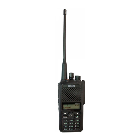
- Page 54 | 以 川) 川』 』 ↓ .1 1 1111111),1111111 11111111 1 1111 11111111 � AIIII Antenna Connector Speaker/ Microphone cover Side Key 2 / Side Key 3 Channel Selector Power / Volume Knob Battery...
- Page 55 Speaker Microphone ”即 “ ..Battery Negative Pole CAPS Battery Positive Pole...
Need help?
Do you have a question about the RDR3600V and is the answer not in the manual?
Questions and answers