
Related Manuals for MAXDATA Belinea 101920


Summary of Contents for MAXDATA Belinea 101920
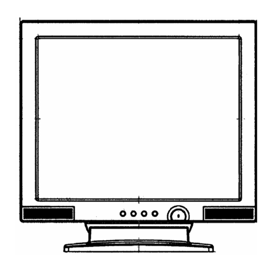
- Page 1 Service Manual Model: Belinea 101920 Art. No. 111912 MAXDATA Systeme GmbH Elbestr. 12-16 45768 Marl / Germany...
-
Page 2: Table Of Contents
Table of Contents CONTENTS PAGE Sections 1. Safety Precaution 2. General Information 3. Supported Modes 4. Video Input Signal 5. Video Input Terminal 6. Theory of Operation 7. OSD Menu Function 8. Specification 9. Critical Parts Specification 10. Block Diagram 11. -
Page 3: Safety Precaution
Belinea Technical Service Manual Safety Precaution WARNING Service should not be attempted by anyone unfamiliar with the necessary precautions on this monitor. The followings are the necessary precautions to be observed before servicing. 1. When managing this monitor, cover with shield plate to avoid to scrach on LCD surface. 2. -
Page 4: Supported Modes
Support Modes *Analog R,G,B Input Resolution H Frequency(KHz) V Frequency(KHz) 720 x 400 31.5 70.1 640 x 480 31.5 59.9 640 x 480 37.5 75.0 800 x 600 37.9 60.3 1024 x 768 48.4 60.0 1024 x 768 56.5 70.1 1024 x 768 60.0 75.0... -
Page 5: Video Input Signal
Belinea Technical Service Manual Video Input Signal Recommended signal are shown below •Video Signal Video level : 0 to 770mV Polarity : positive or Negative Video Input : RGB separated Analog level Sync input : H-Sync(TTL level) V-Sync (TTL level) •Waveform Video input(R.G.B) 700mV... -
Page 6: Video Input Terminal
Video Input Terminal 1. Analog A 15 Pin D-sub connector is used as the input signal connector Pin and input signals are shown in the table below. Pin Description SEPARATE SYNC/ SIGNAL DDC 1/2B PIN NO. GREEN BLUE GROUND or Cable Detect RED GROUND GREEN GROUND BLUE GROUND... - Page 7 Belinea Technical Service Manual 2. Digital 24 Pin DVI-D Interface connector is used as the input signal connector Pin and input signal are shown in the table below. Pin Description SEPARATE SYNC/ SEPARATE SYNC/ PIN NO. DDC 1/2B PIN NO. DDC 1/2B T.MD.S Data 2- T.MD.S Data 2+...
-
Page 8: Theory Of Operation
Theory of Operation 1. DC/AC INVERTER Input voltage : DC 12V Input current : 2.2A (Max) Output current : 7.0mArms (TYP) Frequency(switching) : 60KHz (Max) Output Power : 17W (Typ.) On/off control voltage : 5.0V 2. AC/DC ADATOR This display device shall maintain the specified per formances in the range described below: Frequency : 50/60Hz Voltage : 100 - 240Vac RMS... -
Page 9: Osd Menu Function
Belinea Technical Service Manual OSD MENU FUNCTIONS 1280 x 1024 H : 64.0 V : 60.0 BRIGHTNESS Brightness Miscellaneous Controls the picture brightness. Recall: Restores the image settings to their fac to ry va lues. Contrast OSD Time: Determines the time (in se con ds) to wait Controls the picture contrast. -
Page 10: Specification
Specification SIZE 19” Viewable diagonal Pixel Pitch 0.294 mm LCD Module Contrast Ratio 600 : 1(TYP) Brightness 250 cd/m (TYP) Response Time 25ms (TYP.) Signal R.G.B Analog, Digital TMDS Input Connector 15 pin D-SUB Connector/Digital 24Pin DVI H-Freq 31.0 kHz~80 kHz SYNC V-Freq 56Hz ~75 Hz... -
Page 11: Critical Parts Specification
Belinea Technical Service Manual Critcal Parts Specification 1. LCD Module LTM190EU-L03is a color active matrix TFT (Thin Film Transistor) liquid crystal display(LCD)that uses amorphous silicon TFTs as switching devices.This model is composed of a TFT LCD panel, a driver circuit and a back-light system. The resoution of a 19.0”... - Page 12 MST7131A MC68HC705BD7B FEATURES Ÿ High-quality zoom and shrink scaling engine Auto-Detection/Tune (Compatible with VGA thru SXGA) Ÿ Auto input signal format (SOG, Composite, Ÿ Integrated 8-bit triple-ADC/PLL Separated HSYNC, VSYNC, and DE), and input Ÿ On-screen display controller (OSD) mode (all VESA & IBM modes w/ resolution Ÿ...
- Page 13 Belinea Technical Service Manual PIN DIAGRAM (MST7131A) VSYNC0 AVSS_MPLL AVSS_DVI LVB0M Pin 1 LVB0P GNDP AVSS_DVI VDDP LVB1M LVB1P AVDD_DVI LVB2M LVB2P LVBCKM AVSS_DVI LVBCKP LVB3M LVB3P VDDC AVDD_DVI REXT GNDC AVDD_PLL GNDP AVSS_PLL VDDP LVA0M AVDD AVSS LVA0P BIN0M LVA1M BIN0P LVA1P...
- Page 14 MECHANICAL DIMENSIONS Millimeter Inch Millimeter Inch Symbol Symbol Min. Nom. Max. Min. Nom. Max. Min. Nom. Max. Min. Nom. Max. θ 0° 8° 0° 8° 3.30 0.130 0.26 0.36 0.010 0.014 0.20 0.008 0.14 0.15 0.16 0.006 0.006 0.006 2.72 2.85 2.98 0.107 0.112 0.117 0.50...
- Page 15 Belinea Technical Service Manual 24LC21A MC68HC705BD7B ELECTRICAL CHARACTERISTICS TABLE 1-1: PIN FUNCTION TABLE Maximum Ratings* Name Function Write Protect (active low) ...................7.0V Ground All inputs and outputs w.r.t. V ....-0.6V to V +1.0V Storage temperature ........-65°C to +150°C Serial Address/Data I/O Ambient temp.
- Page 16 ELECTRICAL CHARACTERISTICS TABLE 1-1: PIN FUNCTION TABLE Maximum Ratings* Name Function Write Protect (active low) ...................7.0V Ground All inputs and outputs w.r.t. V ....-0.6V to V +1.0V Storage temperature ........-65°C to +150°C Serial Address/Data I/O Ambient temp. with power applied ....-65°C to +125°C Serial Clock (Bi-directional Mode) Soldering temperature of leads (10 seconds) .....
- Page 17 Belinea Technical Service Manual TABLE 1-3: AC CHARACTERISTICS Vcc= 2.5-5.5V Vcc= 4.5 - 5.5V Parameter Symbol Units Remarks Clock frequency Clock high time 4000 — — HIGH Clock low time 4700 — 1300 — SDA and SCL rise time — 1000 —...
- Page 18 TDA7496L MC68HC705BD7B 2W+2W OUTPUT POWER = 8Ω @THD = 10% V = 14V ST-BY AND MUTE FUNCTIONS LOW TURN-ON TURN-OFF POP NOISE LINEAR VOLUME CONTROL DC COUPLED WITH POWER OP. AMP. NO BOUCHEROT CELL NO ST-BY RC INPUT NETWORK SINGLE SUPPLY RANGING UP TO 15V SHORT CIRCUIT PROTECTION THERMAL OVERLOAD PROTECTION Powerdip (14+3+3)
- Page 19 Belinea Technical Service Manual ABSOLUTE MAXIMUM RATINGS Symbol Parameter Value Unit DC Supply Voltage Maximum Input Voltage Total Power Dissipation (T = 60 C) case Ambient Operating Temperature 0 to 70 Storage and Junction Temperature -40 to 150 Volume CTRL DC voltage PIN CONNECTION Rth with "on board"...
- Page 20 ELECTRICAL CHARACTERISTICS (continued) Symbol Parameter Test Condition Min. Typ. Max. Unit µV Total Output Noise f = 20Hz to 22KHz Play, max volume µV f = 20Hz to 22KHz Play, max attenuation µV f = 20Hz to 22KHz Mute Slew Rate V/µs Input Resistance 22.5...
- Page 21 Belinea Technical Service Manual RC1117X33 MC68HC705BD7B Features Description •Low dropout voltage The RC1117 and RC1117-2.5, -2.85, -3.3 and -5 are low •Load regulation: 0.05% typical dropout three-terminal regulators with 1A output current •Trimmed current limit capability. These devices have been optimized for low voltage •On-chip thermal limiting where transient response and minimum input voltage are •Standard SOT-223, TO-263, and TO-252 packages...
- Page 22 Pin Assignments Tab is Tab is ADJ/ ADJ/ 3-Lead Plastic TO-252 3-Lead Plastic TO-263 = 3 C/W* = 3 C/W* *With package soldered to 0.5 square inch copper area over backside ground plane or internal power plane., can vary from 30°C/W to more than 50°C/W.
- Page 23 Belinea Technical Service Manual Electrical Characteristics Operating Conditions: V 7V, T = 25°C unless otherwise specified. The denotes specifi cations which apply over the specifi ed operating temperature range. Parameter Conditions Min. Typ. Max. Units Reference Voltage, V 1.5V 5.75V, 1.225 1.250 1.275...
-
Page 24: Block Diagram
Analog R·G·B LCD Controller Samsung 19" LCD MST7131A LTM190E1-L03 Micro Controller Volume 24MHz On/Off Audio In Audio Amp Speaker 2W x 2ch TDA7496L Phone Out Title Block Diagram Size Document Number Belinea 101920 <Doc> Date: Wednesday, June 16, 2004 Sheet... -
Page 25: Parts List
PART LIST LOCATION PART NUMBER DESCRIPTION REMARK 304100108402 PCB-DOUBLE,Q19 CN14 3720101983 CONN-M,12507WR-30A00 30 C102 2121040045 CAP-C-C,0.1UF 50V Z Y5V 1608 C103 2121040045 CAP-C-C,0.1UF 50V Z Y5V 1608 C104 2121040045 CAP-C-C,0.1UF 50V Z Y5V 1608 C105 2121040045 CAP-C-C,0.1UF 50V Z Y5V 1608 C106 2121040045 CAP-C-C,0.1UF 50V Z Y5V 1608... - Page 26 LOCATION PART NUMBER DESCRIPTION REMARK C204 2121040045 CAP-C-C,0.1UF 50V Z Y5V 1608 C205 CC7FCA1H220J CAP-CC,22PF 50V J 1608 C206 2014700009 CAP-AL-C,47UF 16V M 6352 C207 CC7FCA1H220J CAP-CC,22PF 50V J 1608 C208 2121040045 CAP-C-C,0.1UF 50V Z Y5V 1608 C209 2121040045 CAP-C-C,0.1UF 50V Z Y5V 1608 C210 2121040045 CAP-C-C,0.1UF 50V Z Y5V 1608...
- Page 27 LOCATION PART NUMBER DESCRIPTION REMARK 3101000376 DI-ZN,Z02W6.2V SMD 3101000376 DI-ZN,Z02W6.2V SMD DTRLS4148 DIODE,CHIP S/W RLS4148 3101000376 DI-ZN,Z02W6.2V SMD 3100100038 DI-AR,KDS226 SMD 3100100038 DI-AR,KDS226 SMD 3100100038 DI-AR,KDS226 SMD 3100100038 DI-AR,KDS226 SMD 3100100038 DI-AR,KDS226 SMD 3100100038 DI-AR,KDS226 SMD 3100100038 DI-AR,KDS226 SMD TT2N3904D TR,SMD 2N3904D TAPPING TT2N3904D TR,SMD 2N3904D TAPPING...
- Page 28 LOCATION PART NUMBER DESCRIPTION REMARK R152 RK1JC0T0473J RES-C,47K 0.063W J 1608 R153 RK1JC0T0101J RES-C,100 0.063W J 1608 R154 RK1JC0T0101J RES-C,100 0.063W J 1608 R155 RK1JC0T0473J RES-C,47K 0.063W J 1608 R156 RK1JC0T0000J RES-C,0 0.063W J 1608 R204 RK1JC0T0103J RES-C,10K 0.063W J 1608 R205 2608201013 RES-C,8.2K 0.1W J 1608...
- Page 29 GASKET EMI 18 X 8 X 12(T) 6128011834 GASKET EMI 26 X 6 X 12(T) 6124038500 HEAT SINK SCALER,VT500 3205001409 WT61P4 PLCC B4204673650 KIT LAB & MAN,Q19/03 MAXDATA/S 631634929001 HI-POT STICKER MAXDATA 6316349353 STICKER MAXDATA L70D/9/Q19(120 6316356578 BACK LABEL, L70P/03(SILVER) MA 6320238600...
- Page 30 EMI SHEET(AL) 30X20 6201341202 STAND ASSY,Q19 MAX BLACK 5001000666 SCR-MC,BIN + MC 3*5 5004000190 SCR-TT,BIN + MC 3*8 6101230400 LIFT BODY BRKT MAXDATA 6101230500 LIFT FRAME MAXDATA 6115028600 HINGE ASSY,19" MAX 6115028100 PIVOT BRKT 19" MAX 6115028200 HINGE BODY MAXDATA...
- Page 31 LCD,LTM190E1-L03 SS 3758000217 CBL-PWR,BK WALL EUROPE 1.8MT C 3758500493 CBL-SGN,1.8MT BLACK 5.5PAI DET 3758500497 AUDIO CABLE 1.8M BLACK 6301191400 PAD PALLET,SW-3 ALL MODEL 6301197100 PAD PALLET,BOTTOM ALL MODEL(80 6301199800 CTN BOX DW-2(W) Q19 MAXDATA 6309030000 PAD CTN,PALLET PBE/U 1517 --29--...
-
Page 32: Schematic Diagram
C140 0.1uF BYPASS R137 OPEN AdjBACKLITE PWM0 AVSS_LPLL PWM1 CON24P_DVI C141 22pF VCPU R136 ST_DET1 KDS226 KDS226 R135 14.318MHz XOUT KDS226 C142 22pF Z6.2V Z6.2V Z6.2V Title 01_MST7131A Size Document Number Belinea 101920 <Doc> Date: Wednesday, June 16, 2004 Sheet... - Page 33 OPEN VCPU 4.7KN OPEN R227 R228 C215 ISP_DAT ISP_CLK 0.1uF R229 R230 24C16 EEPROM_CLK EEPROM_DAT CN24 MENU SELECT DOWN LED_G LED_O POWER CON8P to KEY PAD Title 02_MCU Size Document Number Belinea 101920 <Doc> Date: Wednesday, June 16, 2004 Sheet...
- Page 34 CON7P VCC5V VCC2.5VD C308 C309 C310 C311 RC1117-2.5V 0.1uF 22uF/16V 0.1uF 22uF/16V VCC5V VLCD GFC654 C313 C312 C315 C316 0.1uF 100uF/16V 100uF/16V 0.1uF onPANEL 2N3904 C314 Title 03_POWER Size Document Number Belinea 101920 <Doc> Date: Wednesday, June 16, 2004 Sheet...
- Page 35 TDA7496L C415 0.47UF R412 OUTR C417 C418 R413 1K C421 330uF/16V STBY AUDIOJACK VOLUME R407 MUTE C419 C420 330uF/16V 10uF/16V OUTL CON4P R415 R416 STEREOSW VAROUT_R R410 C410 VAROUT_L C424 330uF/16V Title 04_AUDIO Size Document Number Belinea 101920 Date: Sheet...
-
Page 36: Wave Form
POWER & INVERTER WAVE FORM 1. Q101 DRAIN 2. D103 ANODE 3. D104 ANODE 4. D102 ANODE 5. C116(+) 12V 6. C118(+)5V --34--... - Page 37 7. CN1 8. CN2 9. CN3 10. CN4 --35--...
- Page 38 AD BOARD WAVE FORM 11.CN11 PIN.1(RED) 12. CN11 PIN.13(HS) 13. CN11 PIN.14(VS) 14. CN31 PIN2(OnBacklite) 15. CN31 PIN1(Adj.Backlite) 16. CN14 PIN.22(RXOC+) --36--...
- Page 39 17. CN14 PIN.23(RXOC-) 18. U1 PIN.96(X1) 19. U2 PIN.11(SDA) 20. U2 PIN.12(SCL) 21. U2 PIN.20(HDATA) 22. U2 PIN.7(VDD) --37--...
- Page 40 23. U2 PIN.19(HCLK) 24. U2 PIN.18(HFS) 25. U2 PIN.17(RST) 26. U2 PIN.9(X2) 27. U7 PIN.16(VCC) 28. CN14 PIN.1(VLCD) --38--...
- Page 41 P/N0 FLF1942-06A REV NO. : 0 Adapter DATE : 2004.07.15 REMARKS 11-1. PCB DRAWING (TOP,TOS) FRONTEK CO., LTD --39--...
- Page 42 P/N0 FLF1942-06A REV NO. : 0 Adapter DATE : 2004.07.15 REMARKS 11-2. PCB DRAWING (BOS) *. EYE-LET : CN100 Live and Nutural, TH101, C105 12. INSULATION COVER ( 0.4T ) FRONTEK CO., LTD --40--...
- Page 43 P/N0 FLF1942-06A REV NO. : 0 Adapter DATE : 2004.07.15 REMARKS 13. Adapter circuit FRONTEK CO., LTD --41--...
- Page 44 P/N0 FLF1942-06A REV NO. : 0 Inverter DATE : 2004.07.15 REMARKS 7. Inverter circuit 0 (2012) FRONTEK CO., LTD --42--...
Need help?
Do you have a question about the Belinea 101920 and is the answer not in the manual?
Questions and answers