Table of Contents
Advertisement
SERVICE
Crystal Surround Air Track
HW-C450
Refer to the service manual in the GSPN (see the rear cover) for the more information.
Crystal Surround Air
Track
Model Name : HW-C450
Model Code : HW-C450/EDC
Manual
1. Precaution
2. Product Specification
3. Disassembly & Reassembly
4. Troubleshooting
5. Exploded View & Part List
6. PCB Diagram
7. Schematic Diagram
CONTENTS
Advertisement
Table of Contents

Related Manuals for Samsung HW-C450


Summary of Contents for Samsung HW-C450
- Page 1 Crystal Surround Air Track Model Name : HW-C450 Model Code : HW-C450/EDC SERVICE Manual Crystal Surround Air Track CONTENTS 1. Precaution 2. Product Specification 3. Disassembly & Reassembly 4. Troubleshooting 5. Exploded View & Part List 6. PCB Diagram 7. Schematic Diagram HW-C450 Refer to the service manual in the GSPN (see the rear cover) for the more information.
- Page 2 Asia asia.samsungportal.com Mideast & Africa mea.samsungportal.com © Samsung Electronics Co.,Ltd. Apr. 2010 This Service Manual is a property of Samsung Electronics Printed in Korea Co.,Ltd. Any unauthorized use of Manual can be punished under applicable International and/or domestic law.
-
Page 3: Table Of Contents
Contents 1. Precaution 1-1 Safety Precautions ................... 1-1 1-2 Servicing Precautions ..................1-3 1-3 Precautions for Electrostatically Sensitive Devices (ESDs) ......1-4 2. Product Specification 2-1 Product Feature ....................2-1 2-2 Specifications ....................2-2 2-3 Specifications Analysis ..................2-3 2-4 Accessories ......................2-4 3. Disassembly & Reassembly 3-1 Overall Disassembly &... - Page 4 Contents 7. Schematic Diagram 7-1 Overall Block Diagram ..................7-1 7-2 KEY ........................7-2 7-3 VFD ........................7-3 7-4 U-COM ......................7-4 7-5 INPUT JACK ....................7-5 7-6 DSP ........................7-6 7-7 PWM ........................7-7 7-8 IR AMP ......................7-8 7-9 SMPS .......................7-9...
-
Page 5: Precaution
1 and 5.2 megohms. If there is no return path, the measured resistance should be “infinite.” If the resistance is outside these limits, a shock hazard might exist. See Fig. 1-2 Samsung Electronics... - Page 6 . Use replacement components that have the same ratings, especially for flame resistance and dielectric strength specifications. A replacement part that does not have the same safety characteristics as the original might create shock, fire or other hazards. Samsung Electronics...
-
Page 7: Servicing Precautions
8. Always connect a test instrument’s ground lead to the instrument chassis ground before connecting the positive lead; always remove the instrument’s ground lead last. First read the “Safety Precautions” section of this manual. If some unforeseen circumstance creates a conflict between the servicing and safety precautions, always follow the safety precautions. Samsung Electronics... -
Page 8: Precautions For Electrostatically Sensitive Devices (Esds)
8. Minimize body motions when handling unpackaged replacement ESDs. Motions such as brushing clothes together, or lifting a foot from a carpeted floor can generate enough static electricity to damage an ESD. Samsung Electronics... -
Page 9: Product Specification
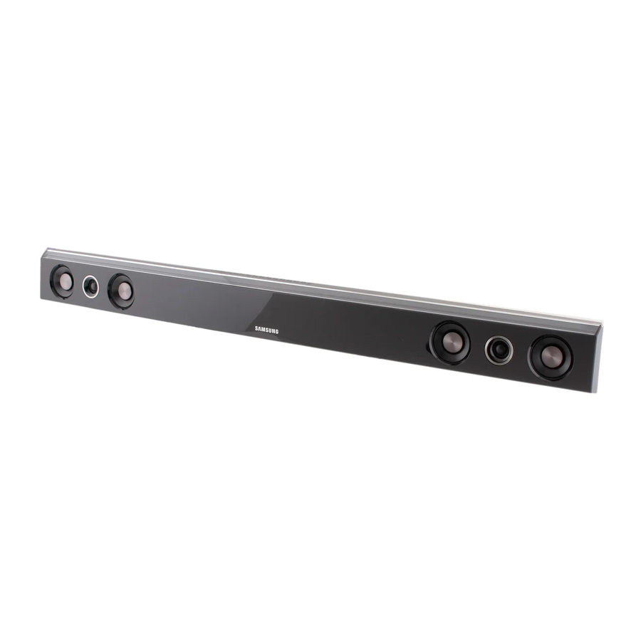
Product Specification 2. Product Specification 2-1 Product Feature 280W (80W x 2 + 120W) 2.1ch, Wireless (Active) DD, DTS 1 analog / 2 opticals Smart Volume II Virtual Surround (Music / News / Movie / Drama / Game / Sports / Pass) 2 Way 3 Spk Samsung Electronics... -
Page 10: Specifications
10% to 75% Main unit 80W/CH, 4Ω, THD = 10%, 1kHz Rated output power Subwoofer 120W, 4Ω, THD = 10%, 100Hz AMPLIFIER Input sensitivity/impedance 450mV/20KΩ S/N ratio (analog input) 70dB Separation (1kHz) 70dB Analog input 20Hz ~ 20kHz (±3dB) FREQUENCY RESPONSE Digital input/48kHz PCM 20Hz ~ 20kHz (±3dB) Samsung Electronics... -
Page 11: Specifications Analysis
Product Specification 2-3 Specifications Analysis Model Name HW-C450 HT-WS1 Photo RMS (10% THD), REF: 1ch 280W 260W Output Power Output Power (ch) 80W x 2 + 120W 80W x 2 + 100W Disc playback Compatible iPod Dock media (select regions only) Wireless Ready Extra USB HOST Features Bluetooth DVD (Video) Progressive Scan (NT/PAL) Virtual Surround Smart Volume Smart Volume II ... -
Page 12: Accessories
TV POWER Remote Control AH59-02196G MENU TOOLS INFO EXIT TV SOURCE TV CH MUTE Batteries 4301-000116 AUTO INPUT POWER PASS LINK CINEMA MUSIC NEWS Optical Cable AH39-00779A Audio Cable AH39-01077A Local Samsung Dealer User’s Manual AH68-02273F Bracket-Wall Mount AH61-02952A Samsung Electronics... -
Page 13: Disassembly & Reassembly
Be careful not to make any scratches as you remove them. 3) Remove the JACK-COVER from the CABINET-REAR. 4) Lift the CABINET-REAR up to separate Power Cord. 5) After disconnecting the Power Cord, lift the CABINET- REAR up completely. Samsung Electronics... - Page 14 2) Separate 2 Speaker Wires from MAIN PCB. 3) Separate the connection between MAIN PCB & SMPS PCB. 4) Remove 5 screws. 1) Remove the screw and separate the Wireless Module. 2) Separate the chassis from the front cover. 3) Separate the VFD Assy. Samsung Electronics...
- Page 15 Disassembly & Reassembly Description Description Photo 1) Separate Speaker (L) & (R). Samsung Electronics...
- Page 16 MEMO Samsung Electronics...
-
Page 17: Troubleshooting
26 of the Replace the Micom (UIC1). UIC1 when Main PCB power is turned on. Check the Check the power(3V) power(3V) at MAIN PCB SMPS PCB CN2 NO.2 P_CON1 NO.18 AC Cable check and replace Replace the connector CN2. Samsung Electronics... - Page 18 4.7KOHM UR24 100OHM UR18 4.7KO UR25 UR28 100OHM 100OH UIC1 UR26 100OHM M_+3.3V 1KOHM U-COM, page 7-4 1/16W M_+3.3V UIC1 1/16W 100OHM REM_DATA 0OHM 1/16W 0OHM 1/16W DSIC5 MAIN PCB Top, page 6-6 DSIC1 <Fig. 4-1> Samsung Electronics...
- Page 19 -18V -25V -13V 5.6V DGND AGND S_GND IR AMP, page 7-8 IRR5 4.7OH K_CON1 -A5V IRR6 4.7OHM IRC1 IRR1 AUDIO_R 2.2KOHM 10UF IRC2 IRR2 AUDIO_L 2.2KOHM 10UF SPK-R SPK-L MAIN PCB Top, page 6-6 <Fig. 4-2> Samsung Electronics...
- Page 20 Replace the DSIC1. Check PWM Input / Output. Check if signal is MAIN PCB PWIC1 measured at pin 15 of PWIC1 of the No.4,10,22 3.3V check Main PCB. Refer to wave pattern image of Fig. 4-5. Replace the PWIC1 Samsung Electronics...
- Page 21 2(-21V), pin 3(-18V), output signal. pin 4, 8(±25V), pin 10(-13V), pin 13, 14(5V). Refer to wave pattern image of Fig. 4-7. Change the MAIN PCB Check the resistance Check the resistance SPK-JACK 1, SPK-JACK2 SPK-JACK 1, SPK-JACK2 CABLE CABLE Samsung Electronics...
- Page 22 INPUT JACK, page 7-5 DGND DIIC1 ADIC1 DSIC3 AINR CKS0 AINL CKS2 CKS1 ADR9 33OHM VCOM ADR7 33OHM AGND MAIN PCB Bottom, page 6-9 SCLK ADR10 33OHM MCLK ADR8 33OHM <Fig. 4-3> LRCK ADR11 33OHM DGND SDTO Samsung Electronics...
- Page 23 DSR20 33OHM DSR21 33OHM DSR19 33OHM DSIC5 D3.3V DSP, page 7-6 0.01OHM 0.01OHM 5000MA 5000MA DSL3 DSL2 DSC8 47UF 6.3V DSR27 1KOHM DSP_RST DGND DSP_MCLK DSR28 100NF 33OHM DSIC1 MAIN PCB Top, page 6-6 <Fig. 4-4> Samsung Electronics...
- Page 24 DVSS PWM1_P PWR3 MSDIN0 PWM1_M MSDIN1 IO_VSS 47OHM MSDIN2 MSDIN3 SBCK IO_VSS PWC11 100NF SLRCK IO_VDD IO_VSS IO_VDD SSDIN0 IO_VSS SSDIN1 RECOUT/LEVELMETER2_P SSDIN2 RECOUT/LEVELMETER2_M PWM, page 7-7 100OHM DGND MAIN PCB Bottom, page 6-9 <Fig. 4-5> Samsung Electronics...
- Page 25 AGND AGND AR18 820OHM 1.5KOHM 10OHM AR15 AC12 AUDIO_L 820OHM 680PF AR10 AR16 SIC5 1.5KOHM 3KOHM 1/10W PWM, page 7-7 0OHM IRR100 0OHM IRR190 0OHM 1N4148WS 1N4148WS AGND AIC1 MAIN PCB Bottom, page 6-9 <Fig. 4-6> Samsung Electronics...
- Page 26 S_GND SPK1 F6645 S_GND +PVDD25V S_GND 6645 5267-02A K_CON1 S_GND IRL2 S_GND UNDEFINED SPK2 IR AMP, page 7-8 6645 S_GND S_GND IRR73 10KOHM IRR74 10KOHM S_GND SPK-R SPK-L MAIN PCB Top, page 6-6 <Fig. 4-7> 4-10 Samsung Electronics...
- Page 27 Fig. 4-8. image of Fig. 4-9. Check the power(5V) pin 6 of Check ADIC1 pin 1, 2 ADIC1 on the Main PCB out / in signal. Refer to wave pattern image of Fig. 4-10. Replace the ADIC1 Samsung Electronics 4-11...
- Page 28 CKS2 CKS1 ADR9 33OH VCOM ADR7 33OH AGND SCLK ADR10 33OH MCLK ADR8 33OH LRCK ADR11 33OH DGND SDTO W_CON1 INPUT JACK, page 7-5 UIC1 DSIC5 AGND DSIC1 MAIN PCB Top, page 6-6 <Fig. 4-8> 4-12 Samsung Electronics...
- Page 29 CKS2 CKS1 ADR9 33OHM VCOM ADR7 33OHM AGND SCLK ADR10 33OHM MCLK ADR8 33OHM LRCK ADR11 33OHM DGND SDTO W_CON1 INPUT JACK, page 7-5 UIC1 AGND DSIC5 DSIC1 MAIN PCB Top, page 6-6 <Fig. 4-9> Samsung Electronics 4-13...
- Page 30 Troubleshooting ADIC1 AINR CKS0 AINL CKS2 CKS1 VCOM AGND SCLK ADR1 MCLK LRCK ADR1 DGND SDTO W_CON1 INPUT JACK, page 7-5 4.7OHM UIC1 DSIC5 AGND DSIC1 MAIN PCB Top, page 6-6 <Fig. 4-10> 4-14 Samsung Electronics...
-
Page 31: Measures To Be Taken When The Protection Circuit Operates
1. Voltage of SMPS’s +, - PVDD (+25V, -25V) is higher or lower than standards. Normal Condition Voltage Range: PVDD (+25V, -25V): about +25V, -25V 2. Over-current occurs to FET. (Over-output or Output short) 3. FET’s temperature exceed 150°C. 4. No supply voltage on GATE DRIVER. Samsung Electronics 4-15... - Page 32 ( Caution: Do not connect the power cord during the test ) Resistance using Tester F/R CH 10kΩ K_CON1 <Table 4-2> In case of large difference with above value → AMP PCB has a problem SPEAKER OUTPUT AIC1 SPK-R SPK-L 4-16 Samsung Electronics...
-
Page 33: Initialization & Update
1) Turn power off. 2) Press for 5 seconds “MUTE” button in remote. 3) Stanby LED becomes OFF, and Volume LED is lighted. 4) If Volume LED becomes OFF, and Stand-by LED becomes ON, initialization is ended. Samsung Electronics 4-17... - Page 34 After updating Sound bar wireless, the Sub-woofer updates automatically. When the Blue and Red LED blink, it means the the Sub-Woofer update is progressing. When the update is finished, the Sound Bar and Sub-woofer will be linked automatically. 4-18 Samsung Electronics...
- Page 35 MEMO Samsung Electronics 4-19...
-
Page 36: Exploded View & Part List
Exploded View & Part List 5. Exploded View & Part List 5-1 Exploded View AC169 W391 HWN01 T0268 T0279 W391 W390 M0014 P001A FL261 W275 MF05A MOD2 SPKLE MK01A FH01A FL261 FL261 SPKRI This Document can not be used without Samsung’s authorization. Samsung Electronics... - Page 37 AH44-00225A DC VSS-HP;HW-C450,HECK-HWC450-F,AC/DC,50 SPKLE AH81-05688A SPEAKER-SYSTEM;BAR SPK,LEFT SPK SPKRI AH81-05689A SPEAKER-SYSTEM;BAR SPK,RIGHT SPK T0268 3903-000407 CBF-POWER CORD;AT,EU,CP2,HOUSING(2P),250 T0279 AH63-02085B COVER-JACK;HW-C450,ABS+PC,2.5,BLACK W275 6003-001561 SCREW-TAPTYPE;BH,+,-,B,M3,L6,ZPC(WHT),SW W390 6003-000276 SCREW-TAPTYPE;BH,+,-,B,M3,L10,ZPC(WHT),S W391 6003-000275 SCREW-TAPTYPE;BH,+,B,M3,L10,ZPC(BLK),SWR Samsung Electronics This Document can not be used without Samsung’s authorization.
-
Page 38: Speaker System
Exploded View & Part List 5-2 Speaker System Wireless Subwoofer Part List Loc. No. Part No. Description;Specification Qty. Remark Wireless AH91-00077J ASSY SPEAKER Subwoofer This Document can not be used without Samsung’s authorization. Samsung Electronics... -
Page 39: Electrical Part List
AH41-01288C PCB-TOUCH KEY HW-C450,FR-4,2 AH41-01289A PCB-VFD HW-C450,FR-4,2 AH61-03066A HOLDER-BUTTON HW-C450,ABS,2.0,WHITE AH74-01030A TAPE-HOLDER HT-WS1,DOUBLE FACE TAPE(3M) AH74-01043A TAPE-HOLDER HW-C450,D/FACE TAPE AH74-01044A TAPE-PCB BUTTON HW-C450,D/FACE TAPE AH90-00482A ASSY MISC-KITTING VFD HW-C450,XAA Samsung Electronics This Document can not be used without Samsung’s authorization. - Page 40 HW-C450,PE,0.1,200,120 AH64-05267A DECORATION-SPK HW-C450,HIPS,2.0,BLACK AH74-01030A TAPE-HOLDER HT-WS1,DOUBLE FACE TAPE(3M) AH74-01032A TAPE-PCB HT-WS1,DOUBLE FACE TAPE(3M) MOD2 AH40-00164A RF MODULATOR NAM-WM51,DSSS,10dBm,3.3~5V, SA P001A AH44-00225A DC VSS-HP HW-C450,HECK-HWC450-F,AC/DC,50 SA M0014 AH94-02511A ASSY PCB MAIN HW-C450,MAIN SA This Document can not be used without Samsung’s authorization. Samsung Electronics...
- Page 41 2007-000043 R-CHIP 1Kohm,1%,1/10W,TP,1608 DR10 2007-000113 R-CHIP 33ohm,5%,1/10W,TP,1608 DR37 2007-000932 R-CHIP 470ohm,5%,1/16W,TP,1005 DS01A 0401-001166 DIODE-SWITCHING BAV20WS-V,150V,250mA,SOD ER19 2007-002899 R-CHIP 10ohm,1%,1/10W,TP,1608 FAN1 3711-000820 HEADER-BOARD TO CABLE BOX,2P,1R,2.5MM,ST FAR22 2007-000082 R-CHIP 3.3Kohm,5%,1/10W,TP,1608 Samsung Electronics This Document can not be used without Samsung’s authorization.
- Page 42 820ohm,5%,1/10W,TP,1608 R2136 2007-000239 R-CHIP 1.5Kohm,1%,1/10W,TP,1608 R227 2007-000086 R-CHIP 5.6Kohm,5%,1/10W,TP,1608 R3A08 2007-000091 R-CHIP 12Kohm,5%,1/10W,TP,1608 R3A13 2007-000100 R-CHIP 68Kohm,5%,1/10W,TP,1608 R419 2007-000882 R-CHIP 4.7ohm,5%,1/10W,TP,1608 R505 2007-000496 R-CHIP 2.2Kohm,5%,1/4W,TP,3216 R509 2007-001179 R-CHIP 8.2Kohm,5%,1/10W,TP,1608 This Document can not be used without Samsung’s authorization. Samsung Electronics...
- Page 43 DBF-1322CD,21.5uH,15%,13.5,13.5 pi AH97-04985A ASSY MANUAL INSERT HW-C450,MAIN_MANUAL,A AH97-05312A ASSY MICOM-NOR-FLASH HW-C450,AH94-02511A AH97-05554A ASSY MICOM-MAIN MICOM HW-C450,AH94-02511 AH91-00083B ASSY SHIELD HW-C450,XEF SNA T0268 3903-000407 CBF-POWER CORD AT,EU,CP2,HOUSING(2P),250 0203-000007 TAPE-FILAMENT T0.15,L55M,TRP Samsung Electronics This Document can not be used without Samsung’s authorization.
- Page 44 2.2nF,10%,50V,X7R,1608 AC28 2203-001607 C-CER,CHIP 0.22nF,5%,50V,NP0,1608 AC850 AH64-05283A CHASSIS-PCB PS-WC450,CHASSIS,STAINLESS,1 AD480 2203-000979 C-CER,CHIP 47nF,10%,50V,X7R,TP,2012 AD480 2203-001386 C-CER,CHIP 100nF,10%,100V,X7R,TP,3216,3. AD480 2203-002494 C-CER,CHIP 470nF,10%,16V,X7R,2012 AD480 2203-006104 C-CER,CHIP 1000nF,10%,50V,X7R,TP,3225,2. AD480 2203-006336 C-CER,CHIP 10000nF,10%,25V,X5R,3216 This Document can not be used without Samsung’s authorization. Samsung Electronics...
- Page 45 CN707 3711-004067 HEADER-BOARD TO CABLE BOX,4P,1R,2mm,ANGL 2305-001016 C-FILM,LEAD-PEF 10nF,10%,630V,TP,12.5x6. D0254 0404-001409 DIODE-SCHOTTKY SR2A0,100V,2000mA,DO-15,T 0401-001099 DIODE-SWITCHING 1N4148WS,75V,150mA,SOD-3 D1S40 0402-000351 DIODE-RECTIFIER 1N4937,600V,1A,DO-41,TP DR01A 0402-001427 DIODE-RECTIFIER ES1D,200V,1A,DO-214AC,TP DR01A 0402-001889 DIODE-RECTIFIER SFAF804G,200V,8A,ITO-220 Samsung Electronics This Document can not be used without Samsung’s authorization. 5-10...
- Page 46 47ohm,5%,1/10W,TP,1608 PRS13 2003-000994 R-METAL OXIDE(S) 33Kohm,5%,2W,AF,TP,3.9x PSCZ2 2201-000129 C-CERAMIC,DISC 0.1nF,10%,1000V,Y5P,-,7x4 0501-000479 TR-SMALL SIGNAL KST42,NPN,350mW,SOT-23,T Q1040 0501-000457 TR-SMALL SIGNAL MMBT2222A/KST2222A,NPN,3 Q1042 0501-000462 TR-SMALL SIGNAL MMBT2907A,PNP,350mW,SOT- Q409 0505-002365 FET-SILICON IRF6645,N,100V,5.7A,0.035ohm 5-11 This Document can not be used without Samsung’s authorization. Samsung Electronics...
- Page 47 WE08 2401-003850 C-AL 1000UF,20%,50V,WT,TP,12.5 X 25,5 X202 2801-004371 CRYSTAL-SMD 12.288MHz,50ppm,SX-1,18pF,50 ZPD2 0401-001090 DIODE-SWITCHING 1SS355,80V,100mA,SOD-323 ZR24 2007-000109 R-CHIP 1Mohm,5%,1/10W,TP,1608 0201-002248 ADHESIVE-A.C.F SMT-GLUE,HT-130D 0.001 SNA 0202-001768 SOLDER-BAR HSE-16,S60S-20,D3,SN/0.5CU/0. 0.329 SNA Samsung Electronics This Document can not be used without Samsung’s authorization. 5-12...
- Page 48 PS-X725,SPK UNIT- AH90-00362K ASSY MISC-KITTING AMP HW-C450,ELS AH97-04102A ASSY AUTO HW-C450,SUBWOOFER AMP_AUTO,AH9 AH97-04104A ASSY MANUAL INSERT HW-C450,SUBWOOFER AMP AH97-05318A ASSY SMD-LED ASSY AH94-02478B AH97-05319A ASSY MANUAL INSERT-LED ASSY HW-C450,AH94 5-13 This Document can not be used without Samsung’s authorization. Samsung Electronics...
-
Page 49: Pcb Diagram
-PVDD-25V 11 W_MCLK WIRELESS MAIN ASSY SMPS ASSY -PVDD-25V 12 DGND MODULE GVDD-12V 13 PT_BCK -A5V 14 PR_LRCK 15 W_TSD2 AGND DGND 19 I_POD DATA 20 I_LRCK DGND POWER_ON 21 I_BCK ST_5.6V 23 WP# U_CON1 P_CON1 24 DGND Samsung Electronics... -
Page 50: Vfd Pcb Top
PCB Diagram 6-2 VFD PCB Top Samsung Electronics... -
Page 51: Vfd Pcb Bottom
PCB Diagram 6-3 VFD PCB Bottom Samsung Electronics... -
Page 52: Key Pcb Top
PCB Diagram 6-4 KEY PCB Top Samsung Electronics... -
Page 53: Key Pcb Bottom
PCB Diagram 6-5 KEY PCB Bottom Samsung Electronics... -
Page 54: Main Pcb Top
PCB Diagram 6-6 MAIN PCB Top W_CON1 K_CON1 UIC1 DSIC5 DSIC1 AIC1 SPK-R SPK-L TP10 Samsung Electronics... - Page 55 VFD_CE S_GND FR OUT W_SDA VFD_RST -PVDD-25V OPEN DGND -PVDD-25V OPEN +VFD_-18V GVDD-12V W_MCLK -VFD_-21V -A5V DGND -VP_-27V AGND PT_BCK OPEN PR_LRCK OPEN W_TSD2 REM_DATA OPEN DGND OPEN DGND OPEN POWER_ON I_POD DATA ST_5.6V I_LRCK I_BCK OPEN DGND Samsung Electronics...
- Page 56 PCB Diagram 6-6-2 Test Point Wave Form TP10 Samsung Electronics...
-
Page 57: Main Pcb Bottom
PCB Diagram 6-7 MAIN PCB Bottom DIIC1 DSIC3 Samsung Electronics... - Page 58 PCB Diagram 6-7-1 Test Point Wave Form 6-10 Samsung Electronics...
-
Page 59: Smps Pcb Top
PCB Diagram 6-8 SMPS PCB Top Samsung Electronics 6-11... - Page 60 PCB Diagram 6-8-1 Pin Connection 1 CN2 Power Signal Control Pin No. Signal ST_5.6V P_ON -A5V GVDD -25V -25V +VFD -VFD VP-27V 6-12 Samsung Electronics...
-
Page 61: Smps Pcb Bottom
PCB Diagram 6-9 SMPS PCB Bottom Samsung Electronics 6-13... - Page 62 MEMO 6-14 Samsung Electronics...
-
Page 63: Schematic Diagram
TX-Module Function and sound field can be controlled by remote controller and keys. S/W Block Diagram RX-Module Pulsus 4558 IRS2092 PS9830B SMPS SPK-S/W IRF6645 Filter Gate Modulator Driver Samsung Electronics This Document can not be used without Samsung’s authorization. -
Page 64: Key
TS06 TS18 TS07 TS19 FUN1 TS08 TS20 DGND 100OHM TS09 TS21 FSP1 100OHM ST5V 100OHM 10KOHM 100OHM DGND KEY_SDA 1/16W ST_BY LED 100OHM KEY_SCL 1/16W KEY_TEST 10KOHM 1/16W DGND This Document can not be used without Samsung’s authorization. Samsung Electronics... -
Page 65: Vfd
MGND2 100OHM VFD_CLK 100OHM VFD_CE VFD_RST V.D V.C TP1 V.RST 1KOHM 1/10W DGND DGND DGND NEW MATERIAL D3.3V CHANGE CODE NO REM_DATA 47OHM MGND1 0.01OHM MGND2 5000MA DGND DGND Samsung Electronics This Document can not be used without Samsung’s authorization. -
Page 66: U-Com
1OHM 1KOHM 100OHM KEY_TEST 1/10W W_SDA 1/16W VFD_RST DGND UP-DATE USB JACK DGND M_+3.3V U_JACK1 1/16W MGND1 100OHM MGND1 REM_DATA 0OHM 1/16W 0OHM 1/16W MGND2 MGND2 UAS21-4K5J0A DGND DGND This Document can not be used without Samsung’s authorization. Samsung Electronics... -
Page 67: Input Jack
CKS1 ADR9 15KOHM 10UF 33OHM VCOM AK_PDN ADR7 33OHM AGND DIR_BCK SCLK ADR10 33OHM DIR_MCLK MCLK ADR8 33OHM DIR_LRCK ADL2 LRCK ADR11 33OHM DGND SDTO 0.05OHM 4.7OHM DGND AGND Samsung Electronics This Document can not be used without Samsung’s authorization. -
Page 68: Dsp
4.7UH 0.01OHM 0.01OHM U_JACK2 5000MA 5000MA DSL3 DSL2 F_TMS F_NTRST DSC8 F_TDI 47UF 6.3V F_TDO D3.3V DSR27 1KOHM DSP_RST DGND DGND DSP_MCLK DSR28 F_TCK 100NF 33OHM F_NEMU0 F_NEMU1 DGND This Document can not be used without Samsung’s authorization. Samsung Electronics... -
Page 69: Pwm
PWC30 100NF 820OHM 680PF SSDIN0 IO_VSS AR10 AR16 1.8KOHM 1.5KOHM SSDIN1 RECOUT/LEVELMETER2_P 3KOHM SSDIN2 RECOUT/LEVELMETER2_M 1/10W 0OHM IRR100 DGND 0OHM IRR190 100OHM 0OHM DGND PS_EXT_MUTE 1N4148WS 1N4148WS DGND AGND Samsung Electronics This Document can not be used without Samsung’s authorization. -
Page 70: Ir Amp
IRR26 0OHM IR_SD_POWER IRF6645 S_GND IRD21 -A5V IRR52 IRD7 6.8KOHM 19-217/R6C-AL1M2VY/3T S_GND 400V -PVDD-25V IRR73 AGND 10KOHM S_GND IRR74 10KOHM IRR19 0OHM S_GND IRR20 0OHM IRR21 0OHM AGND S_GND This Document can not be used without Samsung’s authorization. Samsung Electronics... -
Page 71: Smps
RSA13 USA1 330KF 8.2KF ICE3BR4765J KRC102S RSA7 BAV20W-V 2.2/S12 RSA9 MMSZ5255 ZDS4 ECA2 PC2-A 10uF 50V NHA 5X11 CSA3 0.1uF RSA24 RSA2 RSA1 CSA8 10/S12 10/S12 2.2nF 1nF 400V Samsung Electronics This Document can not be used without Samsung’s authorization. - Page 72 MEMO 7-10 Samsung Electronics...
Need help?
Do you have a question about the HW-C450 and is the answer not in the manual?
Questions and answers
tv comes on sound bar does not