
Related Manuals for Eurotech Catalyst LP


Summary of Contents for Eurotech Catalyst LP
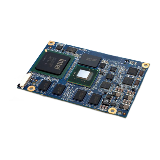
- Page 1 DESIGN-IN GUIDE Catalyst LP High Performance Module Rev 5 – September 2011 – 110125-10005 www.eurotech.com...
-
Page 2: Trademarks
All trademarks both marked and not marked appearing in this document are the property of their respective owners. Document Revision History REVISION DESCRIPTION DATE Preliminary release Aug 2010 Appendix D removed Oct 2010 Initial release Sept 2011 © 2010 Eurotech Inc. -
Page 3: Table Of Contents
Table of Contents Table of Contents Trademarks ..............................2 Document Revision History ..........................2 Table of Contents ............................3 Important User Information ..........................5 Safety Notices and Warnings ......................... 5 Life Support Policy ............................6 Warranty ................................. 6 WEEE ................................6 RoHS ................................ - Page 4 Catalyst LP - Design-In Guide Intel High Definition Audio ..........................23 Power Requirements ............................ 24 Low Power States ........................... 24 Power Supply Architecture ........................25 Power State Signals ..........................27 Mechanical Specifications ..........................31 Mechanical Design ............................31 Mechanical Drawing ..........................31 Total Stack Height ..........................
-
Page 5: Important User Information
Eurotech reserves the right to revise this document and to change its contents at any time without obligation to notify any person of such revision or changes. -
Page 6: Life Support Policy
To avoid damage caused by ESD (Electro Static Discharge), always use appropriate antistatic precautions when handing any electronic equipment. Life Support Policy Eurotech products are not authorized for use as critical components in life support devices or systems without the express written approval of Eurotech. Warranty For Warranty terms and conditions users should contact their local Eurotech Sales Office. -
Page 7: Conventions
When transporting any module or system, for any reason, it should be packed using anti-static material and placed in a sturdy box with enough packing material to adequately cushion it. Warning: Any product returned to Eurotech that is damaged due to inappropriate packaging will not be covered by the warranty. Conventions The following table describes the conventions for signal names used in this document. -
Page 8: Product Overview
The Catalyst LP is available with a variety of operating systems. Support is also available for the Java ™ Virtual Machine and Eurotech’s Everyware... -
Page 9: Features
• Embedded Controller • Optional Trusted Platform Management (Contact Eurotech for details) Memory • Up to 2 GB DDR-2 DRAM • Optional on-board eMMC flash SSD (Contact Eurotech for details) • Integrated system BIOS • Battery-backed real-time clock • External memory support... -
Page 10: Design Checklist
Utilize the Catalyst LP Development Kit for validating your proposed design. For example, if a USB device is to be used on USB port 6, test that device by connecting it to USB port 6 on the Catalyst LP Development Kit. This testing also allows you to validate your OS image with all required drivers loaded. - Page 11 Selecting the same components also allows you to use the drivers Eurotech has already integrated with the OS builds. Follow the design requirements and recommendations Follow the design requirements and recommendations listed in...
- Page 12 Use your Catalyst LP Development Kit Use your Catalyst LP Development Kit to isolate problems. If a problem occurs during bring-up of your carrier board, try to duplicate the problem on the development kit. Prototype bring-up review Review your bring-up process and share lessons learned with your Eurotech representative.
-
Page 13: Development Kit
Kit User Manual (Eurotech document 110125-4000). Related Documents This guide provides details about the various features of the Catalyst LP and about how it creates a system that meets your application needs. It extends the information provided in the Catalyst LP Development Kit User Manual and is intended for hardware design engineers. -
Page 14: Software Specifications
OEM application. It provides industry-standard interfaces that shorten development time, simplify coding, and allow software to be ported from one Eurotech hardware platform to another. ESF is a future option for the Catalyst LP. If your application requires ESF, contact your local Eurotech representative. -
Page 15: Hardware Specifications
Catalyst LP architecture. Intel Atom Processor At the core of the Catalyst LP is the Intel Atom processor N450 (single core) or the Intel Atom processor D510 (dual core). This high-performance architecture offers dual or single core processing with hardware-accelerated 2D/3D graphics display and video processing capabilities. -
Page 16: Trusted Platform Management (Option)
Real-Time Clock, page 50. Flash SSD (option) The Catalyst LP supports an optional on-module eMMC flash SSD. An 8 GB option is available in the standard module configuration. Options of 16 GB and 32 GB are available as custom module configurations. -
Page 17: External Memory Interfaces
USB Mass Storage Device A USB mass storage device can connect to one of nine USB ports on the Catalyst LP. Any USB device that has USB drivers installed on the Catalyst LP can connect to the USB host ports. For a description of these ports, see USB, page 19. -
Page 18: Communications
Design Guidelines, page 35. PCIe Memory Card A PCIe x1 memory card can connect to one of four PCIe x1 slots available on the Catalyst LP. For a description of the PCI Express capability, see Express, page 18. Communications The Catalyst LP supports several industry-standard channels for communication with peripheral and peer devices on the carrier board. -
Page 19: Usb
USB mouse and keyboard are the most common client devices, but you can connect any USB device that has USB drivers installed on the Catalyst LP. USB6, USB7, and USB8 do not include the associated over-current detection signals. When possible, connect these ports to devices on the carrier board. -
Page 20: Carrier I 2 C Bus
SMB addressing. The Catalyst LP provides an external connection on connector J1 to its SMBus with the Intel ICH8M acting as bus master. This bus supports the SMBus 2.0 Specification. In addition, the module supports hardware alerting on the SMBus using the I/O signal SMB_ALERT#. -
Page 21: Display And User Interface
LVDS serial data transmission addresses these issues by providing a high-speed, low-power interface on a single pair of wires per channel. The Catalyst LP supplies a LVDS output to drive a primary display. The following table summarizes the LVDS display output capabilities. -
Page 22: Vga Display
Low Pin Count Interface Specification, Revision 1.1. On the Catalyst LP, the LPC bus connects to the Intel ICH8M, the embedded controller, and an optional TPM. The following diagram illustrates the LPC bus architecture. Catalyst LP ®... -
Page 23: Reset Signals
One of two signals resets the circuitry on the module and carrier board. One signal originates from the module, while the second signal originates from the carrier board. The output signal RST# includes several loads on the Catalyst LP. Include a buffer on the carrier board to drive additional loads. The following table compares the reset signals. -
Page 24: Power Requirements
Embedded system designers using the Catalyst LP should have a clear understanding of how the system design allocates power usage. Create a power budget that takes into account the types of devices that are used with the Catalyst LP. For baseline power consumption for the module, see Power Consumption, page 46. -
Page 25: Power Supply Architecture
Hardware Specifications Power Supply Architecture The architecture of the power supply partitions the power generation across the Catalyst LP and the carrier board. The module requires 5 V and 3.3 V input voltages supplied by the carrier board. It is the responsibility of the carrier board designers to provide input power protection as required by their application. - Page 26 Controller, page 15. RTC Backup Power The Catalyst LP includes a RTC function that retains the system date and time when the system is powered down as long as the 3.3 V “always” power or backup power is provided to the module.
-
Page 27: Power State Signals
Hardware Specifications Power Switch The input signal BTN_ONOFF# (J1 pin B59) controls a power switch included on the Catalyst LP. The function of the BTN_ONOFF# signal is dependent on the embedded controller/BIOS setup and the configuration of the operating system. - Page 28 BTN_ONOFF# input in combination with the operating system. The PM_EN_S0# signal will be de-asserted, and all S0 power rails on the Catalyst LP module will be turned off. The PM_CARRIER_PWRGD signal is not monitored for 10 ms following the de-assertion of PM_EN_S0#.
- Page 29 Table 13, page 24. PM_EN_S0# will be asserted causing all S0 power rails on the Catalyst LP to be turned on. PM_CARRIER_PWRGD will not be monitored for 10 ms after PM_EN_S0# is de-asserted. This provides time for all S0 power rails on the carrier board to be turned on and within specification.
- Page 30 Catalyst LP - Design-In Guide System shutdown initiated by operating system The following diagram shows a system powering at the request of the operating system. The user could initiate this via software control. The operating system will save all information needed and teh system will perform a graceful shutdown.
-
Page 31: Mechanical Specifications
This section describes mechanical and thermal design guidelines for the Catalyst LP. Mechanical Design Mechanical Drawing The following mechanical drawing specifies the dimensions of the Catalyst LP, as well as locations of key components on the board. All dimensions are in inches. Figure 12. -
Page 32: Total Stack Height
Selection of low profile stacking connectors and components minimizes the total stack height of the Catalyst LP and carrier board. The module uses stacking board-to-board connectors to mate with a carrier board. The mating connectors on the carrier board can be either 5 mm or 8 mm stacking height. -
Page 33: Mounting Holes
Insertion and Removal The Catalyst LP connects to the carrier board through two connectors that are in line with each other. A high-density, stacking board-to-board connector carries the data signals, while a smaller 2x7-pin 1 mm-pitch connector carries power. - Page 34 Catalyst LP - Design-In Guide The following diagrams illustrate the location of the three key thermal design interface contact points. TDP 5.5 W (Single Core) TDP 13 W (Dual Core) TDP 2.4 W TDP 2.25 W (across 8 memory devices) Figure 16.
-
Page 35: Carrier Board Design
This carrier board implements many industry-standard interfaces and provides a reference for custom carrier boards optimized for your requirements. This section includes many of the considerations followed in the design of the Catalyst LP Development Kit carrier board. Design Guidelines Design Constraints Increasing reliability is a key consideration in the Catalyst LP design. -
Page 36: Routing Guidelines
Routing Guidelines High-Speed Differential and Single-ended Signals Proper signal routing is critical to a successful carrier board design. The Catalyst LP supports high- speed differential and single-ended signals that require strict routing constraints. Use the following recommendations to route high-speed signals: •... -
Page 37: Power Planes
When installed in a carrier board, the Catalyst LP reads the input signal Cat_LP_Detect (J1 B103) to determine the configuration of the carrier board. This pin must be left open on your carrier board. If the Cat_LP_Detect input is connected incorrectly on the carrier board, the Catalyst LP will not boot. -
Page 38: Test And Debug
SFF style connector. Eurotech highly recommends allowing for access to this connector, in the event you are directed to use this port when working with Eurotech staff. Allow for the size of the mating connector and bend radius of the cable. -
Page 39: Connectors
Connectors Connectors Identifying Connectors The following diagrams illustrate the location and numbering of the connectors on the Catalyst LP. When viewing the module from the component side, connector J1 and connector J2 lie under the module. Figure 18. Connector Location, Top View Figure 19. -
Page 40: Signal Headers
Board connector: 220-pin, stacking board-to-board receptacle, 0.5 mm, Tyco Electronics 3-6318490-6 Carrier board connector: Tyco Electronics 3-1827253-6, 5 mm stacking height Tyco Electronics 3-6318491-6, 8 mm stacking height The Catalyst LP connector J1 mates to the carrier board. Most data signals are provided on this docking connector. Name... - Page 41 Connectors Name Type Description On Module Termination IDE_PDA2 O-LVTTL IDE/PATA address 2 IDE_PDD5 IO-IDE IDE/PATA data 5 IDE_PDD6 IO-IDE IDE/PATA data 6 IDE_PDD1 IO-IDE IDE/PATA data 1 IDE_PDIOR# O-LVTTL IDE/PATA read Ground IDE_PDD2 IO-IDE IDE/PATA data 2 INT_IRQ14 I-LVTTL PU 10kΩ V3.3S IDE/PATA interrupt IDE_PDIORDY I-LVTTL...
- Page 42 Catalyst LP - Design-In Guide Name Type Description On Module Termination A109 Reserved A110 Ground Ground LPCPD# O-LVTTL (Contact Eurotech for details) H_INIT# I-LVCMOS Soft reset for host processor HDA_BITCLK O-HDA Intel HD Audio bit clock HDA_SDATAOUT O-HDA Intel HD Audio data out SLOT0_CMD IO-3.3...
- Page 43 CLK_PCIE_SLOT1 R 33Ω PCIe 1 clock, positive signal B102 CLK_PCIE_SLOT1# R 33Ω PCIe 1 clock, negative signal B103 Cat_LP_Detect I-3.3 Indicates Catalyst LP mode PU 10kΩ V3.3A (See Carrier Board Configuration) B104 PM_EN_S0# O-3.3 Power state indicator PU 10kΩ V3.3A...
-
Page 44: J2: Docking Connector: Power
Carrier board connector: Samtec MW-07-03-G-D-095-085, 5 mm stacking height Samtec MW-07-03-G-D-226-065, 8 mm stacking height The Catalyst LP receives the power input and controls for interfacing with an external power supply on this docking connector. For a description of the Catalyst LP power supply, see... -
Page 45: System Specifications
Power This section includes power specifications for the Catalyst LP. Power Supply The Catalyst LP requires the power inputs and control signals listed in the following table. For a description of the power supply, see Power Supply Architecture, page 25. -
Page 46: Power Consumption
V3.3S Units Dual core Full operation Single core Sleep Power down Performance The Catalyst LP meets the performance specifications listed in the following table. For additional details about the processor, see Core Processor, page 15. Parameter Typ. Units Dual Core... -
Page 47: Pcie Clock Generator
18. CARRIER_I2C_SDA and CARRIER_I2C_SCL do not include termination on the module. Include 10kΩ pull-up resistors to V3.3A on the carrier board. SMBus The Catalyst LP includes an external connection to the SMBus on connector J1. For a description of this bus, see System Management Bus, page 20. -
Page 48: Lvds Display And Backlight
Catalyst LP - Design-In Guide LVDS Display and Backlight The Catalyst LP provides discrete signals and two serial buses to control an LCD and backlight. For a description of these signals, see LVDS Display and Backlight Control, page 21. Symbol Parameter Typ. -
Page 49: General-Purpose Inputs And Outputs
System Specifications General-purpose Inputs and Outputs The Catalyst LP provides four GPIOs. For a description of these signals, see General-Purpose Input Output, page 23. Symbol Parameter Typ. Units GPIO1, GPIO2 (note 25) High-level input voltage Low-level input voltage High-level output voltage -0.2... -
Page 50: Real-Time Clock
Accuracy per month @ 25°C +/-55 Environmental The Catalyst LP is designed to meet the environmental specifications listed in the following table. Note the local ambient temperature of the module is defined by the temperatures at three key thermal design interface contact points. -
Page 51: Appendix A - Reference Information
Appendix A – Reference Information Appendix A – Reference Information Product Information Product notices, updated drivers, support material: www.eurotech.com Intel Information about Intel products, High Definition Audio specification, LPC bus specification: www.intel.com Trusted Computing Group Trusted Computer Group specification: www.trustedcomputinggroup.org... -
Page 52: Appendix B - Board Revision
The revision number is printed on the underside of the printed wiring board. That number is 170125-100Rx. The “x” indicates the revision level of the PWB. Board Revision History The following is an overview of the revisions to the Catalyst LP. Revision A Initial release Revision B SATA 2 and IDE/PATA are no longer mutually exclusive. -
Page 53: Eurotech Worldwide Presence
Web: www.eurotech.com Web: www.parvus.com Web: www.eurotech.com France EUROTECH Tel. +33 04.72.89.00.90 +33 04.78.70.08.24 E-mail: sales.fr@eurotech.com E-mail: support.fr@eurotech.com Web: www.eurotech.com Finland EUROTECH Tel. +358 9.477.888.0 +358 9.477.888.99 E-mail: sales.fi@eurotech.com E-mail: support.fi@eurotech.com Web: www.eurotech.com To find your nearest contact refer to: www.eurotech.com/contacts... - Page 54 EUROTECH HEADQUARTERS Via Fratelli Solari 3/a 33020 Amaro (Udine) – ITALY Phone: +39 0433.485.411 Fax: +39 0433.485.499 For full contact details go to: www.eurotech.com/contacts...
Need help?
Do you have a question about the Catalyst LP and is the answer not in the manual?
Questions and answers