Table of Contents
Advertisement
Quick Links
Advertisement
Table of Contents
Troubleshooting

Related Manuals for BBK DK2810HD


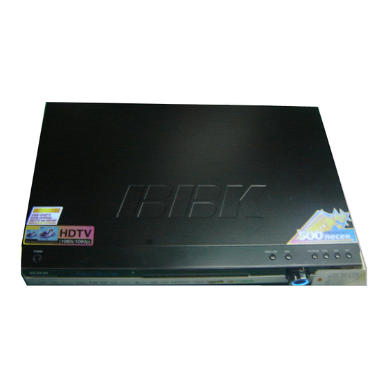
Summary of Contents for BBK DK2810HD
- Page 1 DK2810HD DK2870HD DK2871HD ser vice manual...
-
Page 2: Table Of Contents
Catalog Chapter One About Maintenance 1.1 Safety precautions 1.1.1 Power supply 1.1.2 Precautions for antistatic 1.1.3 Precautions for laser head 1.1.4 About placement position 1.2 Maintenance method 1.2.1 Visualized method 1.2.2 Electric resistance method 1.2.3 Voltage method 1.2.4 Current method 1.2.5 Cutting method 1.2.6 Element substitution method 1.2.7 Comparison method... - Page 3 2.3.7 Preference settings 2.3.8 Parental Control 2.3.9 Initial setupmenu 2.3.10 Resetto defaults 2.3.11 Exit settings menu 2.3.12 Channel d elay set-up 2.3.13 Night mode 2.4 MISCELLANEOUS 2.4.1 Useful notes 2.4.2 Trouble shooting Chapter Three Principle and Troubleshooting Section One Player principle 3.1.1 Brief introductions of function 3.1.2 Block diagram of the player 3.1.3 Introduction to IC of the player...
- Page 4 Chapter Fou Disassembly and Assembly Processr Chapter Cinque PCB board & Circuit diagram Section One PCB board Section Two circuit diagram Chapter Six Bom List Remark: Appearnce silk pirnts of DK2810,DK2870,DK2871 are different.
-
Page 5: Chapter One About Maintenance
Chapter One About Maintenance 1.1 Safety precautions 1.1.1 Power supply When maintenance personnel are repairing DVD players, he should pay special attention to power board with 220V AC and 330V DC which will cause hurt and damage to persons! 1.1.2 Precautions for antistatic Movement and friction will both bring static electricity which causes serious damages to integrated IC. -
Page 6: About Placement Position
1.1.4 About placement position 1. Never place DVD player in positions with high temperature and humidity. 2. Avoid placing near high magnetic fields, such as loudspeaker or magnet. 3. Positions for placement should be stable and secure. 1.2 Maintenance method 1.2.1 Visualized method Directly view whether abnormalities of collision, lack of element, joint welding, shedding welding, rosin joint, copper foil turning up, lead wire disconnection and elements burning up among pins of... -
Page 7: Element Substitution Method
1.2.6 Element substitution method When some elements cannot be judged good or bad, substitution method may de adopted directly. 1.2.7 Comparison method A same good PC board is usually used to test the correct voltage and waveform. Compared these data with those tested through fault PC board, the cause of troubles may be found. Through the above maintenance method, theoretical knowledge and maintenance experience, all difficulties and troubles will be readily solved. -
Page 8: Features
Chapter Two Functions and Operation Instructions 2.1 Features Formats: #Digital video playback of DVD-Video, Super VCD and VCD formats #MPEG-4 compatibility: playback of DivX3.11, DivX4, DivX5, DivXPro and XviD formats #Playback of music discs in DVD-Audio format #Playback of musical compositions in CD-DA and HDCD formats #Playback of compressed musical files in Mp3 and WMA formats #Playback of karaoke-discs in DVD, VCD and CD+G formats #Playback of photo albums, recorded in Kodak Picture CD and JPEG digital formats... -
Page 9: Controls And Functions
2.2 Controls and functions 2.2.1 Front panel controls STANDBY/POWER button REW button Press to switch the device on/into stanby Press to fast reverse/radio station tuning. OPEN/CLOSE button FWD-button Press to open/close the disc tray Press to fast forward/radio station tuning. HDMI Button VFD display window. -
Page 10: Vfd Display General View
Center speaker input(output from the Left Surround speaker input(output from build-in amplifier) the build-in amplifier) Subwoofer input(output from the build-in Right Surround speaker input(output from amplifier) the build-in amplifier) 2.2.3 VFD display general view CD-,VCD-or SVCD-disc Dolby Digital DVD-disc Programmed radio station AM/FM Friquency Radio tuning mode... -
Page 11: Function Settings
BOOST button Numeric buttons Press to bass boosting. ST/5.1 button BROWSER button Press to switch between STEREO/5.1CH. Press to turn on/off the browser function. TREBLE+/- button JOG DIAL wheel Press to adjust the tone. Functions are set manually. Default ECHO button function: ZOOM. -
Page 12: Language Settings
#Options: Off, Russian, English, Estonian, Latvian, Kazakh, Romanian, Belarusian, Ukrainian and Chinese. #Default option: Off. #Selection of other languages: select the OTHERS item using the Jog Dial and press OK. Enter the language code using numeric buttons and press OK. #If the language you selected is not recorded on 2. -
Page 13: Sound Settings Menu
2.3.4 Sound settings menu 1. Mixer A) Configuration: setting of the mode for conversion of the 5-channel signal to stereo signal #Options: Stereo, 5.1. #Default option: 5.1.. #5.1 mode must be supported by the disc F) Delay of the channel: set-up of signal delay in Number of muic accompaniment channels speaker channels(central, rear and subwoofer). -
Page 14: Playback Settings
#Default option: 48 kHz 16 bit. 5.Repeat: file repeat mode 3.Sound correction #Options: Off, Single, All. A) equalizer: equalizer modes #Default option: Off. #Options: Rock, Pop, Live, Dance, Techno, 6.Load effect: type of transition from one JPEG Classic, Soft. file to another #Default option: Off. -
Page 15: Parental Control
3.Background: selection of and image as TV 2.3.10 Reset to defaults screen wallpaper #Resetting all settings and restoring default #Options: Standard, Saved options, except age restrictions level and #Default option: Standard. password. 4.Screensaver: screen saver on/off #Options: On, Off. #Default option: On. 5.Jog Dial #Options: Zoom, Step, Fast, Skip, Volume. -
Page 16: Night Mode
Fig.3. Small area Delay of central channel=0 L= R C 2.3.13 “ Night”mode The Dolby Digital system provides an Fig.3. Determine Fig.2. Determine delay extremely broad dynamic range of playback delay value as to Dolby value as to Dolby Pro Logic sound-from gentle to roaring. -
Page 17: Miscellaneous
Dolby Digital Dolby Pro Logic surround Mono channel with limited frequency Rear channel Stereo 20 Hz-20 kHz range(100Hz-7 kHz) Low-frequency Available,20-120 Hz channel(subwoofer) Sound field distribution Muitivariate From left to right, from right to left, from front to rear, from rear to front 6 independent channels, each 4 segmented channels. - Page 18 Sign of trouble Cause of trouble Actions to eliminate the trouble 1.Poor audio cable connection 1.Make proper connection. No sound 2.Disc dirty or damaged. 2.Clean the disc. 3.Sound disabled by the MUTE button. 3. Press the MUTE button. 1.Poor video cable connection. 1.Make proper connection.
-
Page 19: Chapter Three Principle And Troubleshooting
Chapter Three Principle and Troubleshooting Section One Player principle 3.1.1 Brief introductions of function This player adopts brand new model with new generation DVD decode chip. With built-in Dolby decoder and HDMI high definition decoder, vivid surround sound system, supporting 1080I high definition format output, it brings you personal theater effect. - Page 20 Optical/coaxial Optical/coaxial Progressive/comp Karaoke AUX_IN TUNER S terminal HDMI output Composite video SCART L/R OUT input onent output output MIC1/MIC2 AUXL/AUXR TU_L/TU_R RDS_MPX VIDEO_COMP Cr/Pr VIDEO_COMP ROUTX TX2+ VIDEO SPDIF Buffering amplify Cb/Pb VIDEO_C LOUTX TX2- 4558 Digital audio VIDEO_Y TX1+ receiving Cs8415A TX1-...
-
Page 21: Introduction To Ic Of The Player
3.1.3 Introduction to IC of the player Introduction to IC of the player is shown as in the following table: Name of PCB semi- IC Type Location Number Function manufactured goods AM5888S Servo Driving AT24C04 EEPROM MT1389EE/S Decode Chip K4S641632K-UC60 64M SDRAM RT9701 USB Power Switch... -
Page 22: Section Two Unit Circuit Principle
Section Two Unit Circuit Principle 3.2.1 Introduction to laser head Function introduction to laser head flat cable is shown as the following table: Signal flow Name DVD disc CD disc No disc Function description direction Input loader 2.52 2.34 0.46 Focus error signal is added to two sides of pick-up focus coil Input loader... -
Page 23: Decode Cirauit
Signal flow Name DVD disc CD disc No disc Function description direction High frequency overlapping signal produces Input loader 5.04 5.04 5.02 laser with different wave length inside loader Blanking unused 0.01 LD-DVD Input loader 2.21 DVD laser power control signal unused 0.01 0.01... - Page 24 SDCLK SDCKE DRAS A0~A20 MT 1389 SDRAM FLASH DQM0 AD0~AD7 DQM1 DQ0~DQ15 URST MA0~MA11 Clock EEPROM 1.8V voltage Reset Circuit stabilization 24C02 Figure 3.2.2.1 Block diagram of decode circuit 2. Working principle: this decode circuit is mainly composed by MT1389, SDRAM and FLASH. The important conditions for decode circuit working are: 1 Reset: for detail working principle, you can refer to reset circuit working principle.
-
Page 25: Servo Circuit
3.2.3 servo circuit 1.Servo system of this player adopts SANYO HD62 chip and MTK decode scheme MT1389S+FLASH +SDRAM . And servo circuit is mainly composed by front signal processing and digital servo processing IC MT1389 and driving circuit AM5888. MT1389 is also main part of decode circuit. -
Page 26: Disc Identification Circuit
corresponding servo control signal and separately output focus, track, main axis, feed and other servo control signals from pin 41, 40, 36 and 37 in MT1389. After passing integrating circuit composed by resistance and capacitor, focus, track, main axis and feed signals are separately sent to servo driving circuit to have driving amplify. -
Page 27: Main Axis Braking Control Circuit
now IOA is low level input loader to make loader in the state of reading DVD, through detecting laser power feedback signal, MT1389 analyses whether the preliminary judgment is correct (disc is defaulted DVD). When detecting correct preliminary judgment, loader runs in the state of reading DVD; when detecting incorrect preliminary judgment, MT1389 outputs a high voltage signal from its pin 54, Q5 and Q4 are on, Q3 is cut off, laser receiver tube inside loader selects VCD channel, now IOA is high level input loader to make loader in the state of reading VCD. -
Page 28: Tray Open/Close Driving Circuit
2. Working principle: To prolong the service life of electric machine and decrease the influence of start-up concussion current to the machine, when there is disc in, the development personnel design the main axis electric machine in running state always. Even though “STOP” button is pressed, disc will not stop running immediately. -
Page 29: Mute Circuit
DV33 URST# R117 TC81 16uF/10V R116 2SC1815-YS 1N4148 Figure 3.2.7.1 Reset circuit diagram 2. Working principle: after power on, voltage of DV33 increases to 3.3V, main chip power supply is normal. Now, voltage of TC81 to DV33 cannot change suddenly to make base electrode of Q80 has current flow in, Q80 is saturation on, URST is low level. -
Page 30: Video Circuit
3.2.9 Video circuit 1. Video circuit block diagram is shown as the following figure 3.2.9.1: S-VIDEO V-OUT V-OUT MT1389 Component video SCART terminal Figure 3.2.9.1 Video circuit block diagram 2.Brightness signal, colour difference signal, CVBS signal and component video signal after being decoded by MT1389 are sent out to the corresponding terminal for output after lowpass filtering and clipping. -
Page 31: Audio Power Amplifying Circuit Block Diagram
3.2.10 Audio power amplifying circuit block diagram 1. Audio power amplifying circuit block diagram is shown as the following figure 3.2.10.1: AUXR Surround left/right channel N507 AINR External audio input on power amplifier board, TAS5112 N509 AUXL subwoofer channel output SDA _AD N505 N502... - Page 32 HOUSE Source HDMI Sink Video TMDS Chnanel 0 Video TMDS Chnanel 1 Audio Audio TMDS Chnanel 2 Control Status Control Status TMDS Clock Chnanel Display Data Channel 3.2.1 .1 HDMI Block Diagram 2. Working principle: ordinary audio video output is same with other ordinary DVD, which make initial process for analog audio and video signal decoded by MT1389S and send them to analog output terminal.
-
Page 33: Control Panel Components
3 Definition of HDMI Type A jack is shown as follows: Signal Assignment Signal Assignment TMDS Data2+ TMDS Data2 Shield TMDS Data2- TMDS Data1+ TMDS Data1 Shield TMDS Data1- TMDS Data0 TMDS Data0 Shield TMDS Data0- TMDS Clock+ TMDS Clock Shield TMDS Clock- Reserved (N.C. -
Page 34: Power Circuit
2. Working principle: panel is mainly composed of VFD screen, drive chip TP6317, remote controller IR receiver, digital potentiometer, button and indicator light. VFD is a vacuum fluorescence display screen and the working principle is the same with that of CRT TV set, that is, emit light and display through electron bombarding fluorescent powder. - Page 35 2.Working principle: Power supply is divided into two channels to supply power. One channel supplies power for decode board and other small power IC with small power and low voltage; the other channel supply power for power amplifier with high voltage and large power. But the design method is the same and the structure is as above: (1) Electric wire netting filtering circuit as there are various of magnetic radiation, input...
-
Page 36: Section Three Troubleshooting Cases
Section Three Troubleshooting Cases 3.3.1 Troubleshooting Cases Example 1 Symptom Power not on Description Plug unit, power standby indication light is not on, power on is not available. Analysis and troubleshooting: detect power board, 5V and 3.3V voltages are all normal. Detect power supply of decode board MT1389 chip are 3.3V and 1.8V, which are normal. - Page 37 Example 5 Symptom: sound receiving has no sound Description: when receiving sound, connect left and right channels of amplifier, but there are no sound output. Analysis and troubleshooting: first turn on sound receiving, use probe of oscillograph to separately check pin 3 and 13 of N501, and it is found that there is audio signal . Then check pin 4 of N502, and there is no audio signal.
-
Page 38: Flow Chart Of Troubleshooting
3.3.2 Flow chart of troubleshooting 1. Troubleshooting flow chart of power not on is shown in figure 3.3.2.1 Player not power on Whether Whether power supply of power L506 and D510 are Replace L506 D510 board +5V is conductive normal Whether Whether power supply of decode... - Page 39 2 Troubleshooting flow chart of amplifier has no output is shown in figure3.3.2.2 Amplifier has no output Whether Whether there is output in sound 28V power supply Check 28V power branch receiving or testing is normal MIC state Whether Whether Check overcurrent pin 25-31 signals of PWM signal from TAS5508...
- Page 40 4 Troubleshooting flow chart of amplify external input has no sound is shown in figure 3.3.2.4 External input has no sound Whether Whether pin 34 and 38 of N508 mix terminal has Replace N508 output have output Normal Whether pin 5 and 14 of N505 Check mix input terminal have signal Whether...
- Page 41 5 Troubleshooting flow chart of " no disc reading" is shown in figure 3.3.2.5 no disc reading After tray closes to Whether pick-up lights right position, whether Replace pick-up pick-up has motions Whether Whether pin 213 voltage of Check power supply pick-up +5V power supply Check loader 5P flat cable Mt1389 is 0V...
- Page 42 6 Troubleshooting flow chart of player not power on is shown in figure 3.3.2.6 Player not power on Whether Whether indication light of +5V of power board Check power supply circuit panel is on is normal Replace panel light emitting diode Whether Whether STBY signal of main...
- Page 43 Section Four Waveform diagram This section collects signal waveform diagram of audio, video and each unit circuit with the purpose to help servicing personnel to judge where trouble lies in accurately and quickly to improve servicing skills. For the difference of oscillograph's type, model and tuner, a certain difference may exist, so the servicing personnel are expected to pay more attention to check in daily operation.
- Page 44 3. DMO signal (when there is main axis rotation) waveform diagram of pin 36 of N3 (MT1389) 4. FMO signal (when there is feed) waveform diagram of pin 37 of N3 (MT1389) 5. TRO signal (when there is trace) waveform diagram of pin 40 of N3 (MT1389) - 40 -...
- Page 45 6. FOO signal (when there is focus) waveform diagram of pin 41 of N3 (MT1389) 7. Waveform diagram of pin 29 (when no disc in) of N83 (FLASH) 8. Waveform diagram of pin 38of U81 (SDRAM) - 41 -...
- Page 46 27M clock signal waveform diagram 10. 1KHZ signal waveform diagram. It is suggested to use test disc, if not, the tested waveform will change at any time to affect judgment. 11. Contrast waveform diagram of reset signal and 3.3V voltage path 2 - 42 -...
-
Page 47: Section Five Function Introduction To Ic
Section Five Function Introduction to IC 3.5.1 Function introduction to MT1389S 1. General Description MediaTek MT1389S is a DVD system-on-chip (SOC) which incorporates advanced features like MPEG-4 video decoder, WMV-9 decode, high quality TV encoder, USB2.0, MS/SD/MMC reader, state-of-art de-interlace processing, SACD2.0 decoder, ATRAC audio file support, built-in DVB-T decoder, and HDMI1.2 compatible transmitter. - Page 48 support current multimedia contents. The MT1389S provides the interface for the 3-in-1 card reader, which supports Memory-Stick, Secure Digital Memory Card, and Multimedia Card, to connect with the mainstream digital camera FLASH cards. For the USB application, we adopt USB2.0 High speed specification to reach rich-contents transferring.
- Page 49 (3) Speed Performance on Servo/Channel Decoding DVD-ROM up to 4XS CD-ROM up to 24XS (4) Channel Data Processor Digital data slicer for small jitter capability Built-in high performance data PLL for channel data demodulation EFM/EFM+ data demodulation Enhanced channel data frame sync protection & DVD-ROM sector sync protection (5) Servo Control and Spindle Motor Control Programmable frequency error gain and phase error gain of spindle PLL to control spindle motor on CLV and CAV mode...
- Page 50 Support Nero-Digital Support DivX Ultra Support WMV9 VC-1 Smooth digest view function with I, P, and B picture decoding Baseline, extended-sequential and progressive JPEG image decoding Support CD-G titles (10) Video/OSD/SPU/HLI Processor Arbitrary ratio vertical/horizontal scaling of video, from 0.25X to 256X Scaler for standard-definition to high-definition conversion 65535/256/16/4/2-color bitmap format OSD Automatic scrolling of OSD image...
- Page 51 Pink noise and white noise generator Karaoke functions - Microphone echo - Microphone tone control - Vocal mute/vocal assistant - Key shift up to +/- 8 keys - Chorus/Flanger/Harmony/Reverb Channel equalizer 3D surround processing including virtual surround and speaker separation (13) TV Encoder Four 148MHz/12-bit DACs Support NTSC, PAL-BDGHINM, PAL-60...
- Page 52 Support input & output maximum size: 4096x4096 JPEG case Input memory layout of source images must be scan line based Deal with one block line (height:8 / 16) each round Input maximum size: 65535x65535 Output maximum size: 4096x4096 Support a output scaling window at arbitrary location in an output frame buffer Y / Cb / Cr separated (17) External Interface USB2.0 High Speed (Host/Device)
- Page 53 Main Alt. Type Description Analog Input DC coupled sub-beam RF signal input A Analog Input DC coupled sub-beam RF signal input B 1) DC coupled sub-beam RF signal input C Analog Input 2) 3 beam satellite PD signal negative input 1) DC coupled sub-beam RF signal input Analog Input 2) 3 beam satellite PD signal positive input D...
- Page 54 Main Alt. Type Description Analog output Tracking error monitor output TEZISLV Analog output TE Slicing Level Analog Servo Interface ( 6 ) RFVDD3 Power Analog Power RFRPDC Analog output RF ripple detect output RFRPAC Analog Input RF ripple detect input(through AC-coupling) HRFZC Analog Input High frequency RF ripple zero crossing...
- Page 55 Main Alt. Type Description 55,93, DVDD18 Power 1.8V power pin for internal digital circuitry 142,160, 212 DVSS18 Ground 1.8V Ground pin for internal digital circuitry 65,96,118, 131,145,156, DVDD3 Power 3.3V power pin for internal digital circuitry 90, 148 DVSS33 Ground 3.3V Ground pin for internal digital circuitry Micro Controller and Flash Interface ( 47 ) 1) Microcontroller address 8...
- Page 56 Main Alt. Type Description Inout Microcontroller address 15 HIGHA7 4~16MA, SR Inout Microcontroller address/data 7 4~16MA, SR Inout Microcontroller address/data 6 4~16MA, SR Inout Microcontroller address/data 5 4~16MA, SR Inout Microcontroller address/data 4 4~16MA, SR Inout Microcontroller address/data 3 4~16MA, SR Inout Microcontroller address/data 2 4~16MA, SR...
- Page 57 Main Alt. Type Description Inout IOA5 4~16MA, SR Microcontroller address 5 / IO Inout IOA6 4~16MA, SR Microcontroller address 6 / IO Inout IOA7 4~16MA, SR Microcontroller address 7 / IO Inout 4~16MA, SR Flash address 16 Inout 4~16MA, SR Flash address 17 Inout IOA18...
- Page 58 Main Alt. Type Description Inout IOOE# 4~16MA, SR Flash output enable, active low / IO Inout IOWR# 4~16MA, SR Flash write enable, active low / IO SMT, PU Inout IOCS# 4~16MA, SR Flash chip select, active low / IO Inout UWR# 4~16MA, SR Microcontroller write strobe, active low...
- Page 59 Main Alt. Type Description Inout 1) Microcontroller port 3-0 UP3_0 4MA, SR 2) 8032 RS232 RXD SMT, PU Inout 1) Microcontroller port 3-1 UP3_1 4MA, SR 2) 8032 RS232 TXD SMT, PU Inout 1) Microcontroller port 3-4 UP3_4 RXD SCL 4MA, SR 2) Hardwired RD232 RXD SMT, PU...
- Page 60 Main Alt. Type Description 1) GPIO9 2) C3 (1st set of CCIR656) Inout 3) YUVCLK (2nd set of CCIR656) GPIO9 YUVCLK 2~8MA 4) MS_D3 (1st set of MS_SD) 5) MCDATA 6) ASDATA4 7) AUDIO_MUTE 1) GPIO10 Inout 2) C2 (1st set of CCIR656) GPIO10 3) SD_D3 (1st set of MS_SD) 2~8MA...
- Page 61 Main Alt. Type Description 1) AUDIO DAC Sub-woofer channel output 2) While internal AUDIO DAC not used: GPIO Output a. GPIO b. ALRCK 1) AUDIO DAC Right Surround channel output 2) While internal AUDIO DAC not used: GPIO Output a. GPIO b.
- Page 62 Main Alt. Type Description ADACVSS3 Ground Ground pin for AUDIO DAC circuitry ADACVDD3 Power 3.3V power pin for AUDIO DAC circuitry Video Interface ( 14 ) DACVDDC Power 3.3V power pin for VIDEO DAC circuitry VREF Analog Bandgap reference voltage Analog Full scale adjustment (suggest to use 560 ohm) DACVSSC...
- Page 63 Main Alt. Type Description 1) TS SYNC Inout 2) C6 (1st set of CCIR656) TS_SYNC GPIO 2~8MA 3) Digital Video output Y bit 2 (2nd set of CCIR656) 4) MCDATA 5) GPIO 1) TS Clock Inout 2) C7 (1st set of CCIR656) TS_CLK GPIO 2~8MA...
- Page 64 Main Alt. Type Description 1) TS DATA4 2) Y3 (1st set of CCIR656) Inout 3) MS DATA2(IO) (2nd set of MS_SD) TS_DATA4 MS_D2 2~8MA 4) Digital Video output C bit 0 (2nd set of CCIR656) 5) SPDF_BCK 6) HSYNC or VSYNC 7) GPIO 1) TS DATA3 2) Y4 (1st set of CCIR656)
- Page 65 Main Alt. Type Description Inout I. SD D0 (Both set of MS_SD) GPIO22 2~8MA II. Digital Video output C bit 7 (2nd set of CCIR656) III. GPIO22 IV. INT0# USB2.0 ( 9 ) USB_DP Analog Inout USB port DPLUS analog pin USB_DM Analog Inout USB port DMINUS analog pin...
- Page 66 Main Alt. Type Description AGND33_VPLL Analog Power 3.3V GND FOR HDMI TX MISC ( 7 ) Input 4MA, SR Microcontroller ICE mode enable SMT, PD Input PRST# 4MA, SR Power on reset input, active low SMT, PU Input IR control signal input SR, SMT XTALO Output...
- Page 67 Main Alt. Type Description output RA11 2~16MA, SR DRAM address bit 11 SMT, PU, PD output 2~16MA, SR DRAM clock enable SMT, PU, PD output RCLK 2~16MA, SR Dram clock SMT, PU, PD output 2~16MA, SR DRAM address 3 SMT, PU, PD output 2~16MA, SR DRAM address 2...
- Page 68 Main Alt. Type Description output RAS# 2~16MA, SR DRAM row address strobe, active low SMT, PU, PD output CAS# 2~16MA, SR DRAM column address strobe, active low SMT, PU, PD output RWE# 2~16MA, SR DRAM Write enable, active low SMT, PU, PD output DQM1 2~16MA, SR...
- Page 69 Main Alt. Type Description Inout RD15 2~16MA, SR DRAM data 15 PU, PD Inout 2~16MA, SR DRAM data 0 PU, PD Inout 2~16MA, SR DRAM data 1 PU, PD Inout 2~16MA, SR DRAM data 2 PU, PD Inout 2~16MA, SR DRAM data 3 PU, PD Inout...
- Page 70 commercial applications where low-power and low-voltage operation are essential. The AT24C02 is available in space-saving 8-lead PDIP, 8-lead MAP, 8 lead TSSOP and 8-ball dBGA2 packages and is accessed via a 2-wire serial interface. In addition, the entire family is available in 2.7V (2.7V to 5.5V) and 1.8V (1.8V to 5.5V) versions. 2.
- Page 71 3.5.3 Function introduction to 29LV160BE 29LV160BE is a 16Mbit FLASH memorizer, and the damage of U214 may cause troubles, such as power not on, no disc reading and power on picture mosaic. Pin function is shown as the following table: Name Function Voltage (when no disc)
- Page 72 Data bus MA11 Address bus VDDQ 3.3V power supply Blank Data bus Clock enable signal Data bus System clock input Data input/output VSSQ Ground UDQM screen-shielded signal Data bus Blank 3.3V power supply Ground Data input/output screen-shielded LDQM Data bus...
- Page 73 ◆ Separating power of Vcc1 and Vcc2 is to improve power efficiency by a low supply voltage for tracking, focus, and spindle. ◆ Level shift circuit built-in. ◆ Thermal shut down circuit built-in. ◆ Mute mode built-in. ◆ Dual actuator drivers: A general purpose input OP provides differential input for signal addition.
- Page 74 VCC2 Vcc for power block of spindle, tracking and focus No Connection VCTL Speed control input of tray driver Ground VINLD Input for spindle driver No Connection TRB_2 Connect to external transistor base VINTK Input for tracking driver BIAS Input for reference voltage MUTE Input for mute control 3.5.6 function introduction to 4558...
- Page 75 Description PIN No Symbol Output 1 1OUT Inverting Input Pin 1 1IN– Non-Inverting Input Pin 1 1IN+ Negative Power Supply VCC– Non-Inverting Input Pin 2 2IN+ Inverting Input Pin 2 2IN– Output 2 2OUT 3.5.7 function introduction to CD4052 1. Description The CD4052B analog multiplexers is digitally-controlled analog switches having low ON impedance and very low OFF leakage current.
- Page 76 ◆ 10% Tested for Quiescent Current at 20V ◆ Maximum Input Current of 1mA at 18V Over Full Package Temperature Range, 100nA at 18V and 25 ℃ ◆ Break-Before-Make Switching Eliminates Channel Overlap 3.5.8 function introduction to SAA6588 1. DESCRIPTION Today most FM radio stations in Europe and meanwhile also many FM/AM radio broadcasting stations in the USA transmit the inaudible European RDS (Radio Data System) or the USA RBDS (Radio Broadcast Data System) informations respectively.
- Page 77 2. FEATURES ◆ Integrated switched capacitor filters ◆ Demodulation of the European Radio Data System (RDS) or the USA Radio Broadcast Data System (RBDS) signal ◆ RDS and RBDS block detection ◆ Error detection and correction ◆ Fast block synchronization ◆...
- Page 78 VDDA analog supply voltage (5 V) VSSA analog ground (0 V) multiplex input signal Vref reference voltage output SCOUT band-pass filter output comparator input LVIN level input 3.5.9 function introduction to 5340 1. DESCRIPTION The CS5340 is complete analog-to-digital converter for digital audio systems. It performs sampling, analog-to-digital conversion and anti-alias littering, generating 24-bit values for both left and right inputs in serial form at sample rates up to 200 kHz per channel.
- Page 79 SDOUT Serial audio data output Digital power SCLK Serial clock LRCK Left right clock /RST Reset AINL Analog input L Quiescent voltage AINR Analog input R Analog power REF_GND FILT+ Positive voltage reference Mode selection 1 3.5.10 function introduction to TLV272 1.
- Page 80 ◆ Supply Voltage Range . . . 2.7 V to 16 V ◆ Supply Current . . . 550 µA/Channel ◆ Input Noise Voltage . . . 39 nV/vHz ◆ Input Bias Current . . . 1 pA ◆ Specified Temperature Range 0°C to 70°C .
- Page 81 ◆ 5-V Tolerant Inputs ◆ Supports Two PLL Input Modes: ◆ Crystal Mode ◆ No-Crystal Mode 3. PIN DESCRIPTION Symbol Description VRA_PLL Voltage reference for PLL analog supply 1.8 V PLL_FLT_RET PLL external filter return PLL_FLTM PLL negative input PLL_FLTP PLL positive input AVSS Analog ground...
- Page 82 SDIN4 Serial audio data 4 input SDIN3 Serial audio data 3 input SDIN2 Serial audio data 2 input SDIN1 Serial audio data 1 input PSVC Power supply volume control PWM output VR_DIG Voltage reference for digital core supply 1.8 V DVSS Digital ground DVSS...
- Page 83 PWM_HPMR PWM right channel headphone (differential -) PWM_HPPR PWM right channel headphone (differential +) MCLK MCLK is a 3.3-V clock master clock input RESERVED Connect to digital ground 3.5.12 function introduction to TAS5112DFD 1. DESCRIPTION The TAS5112 is a high-performance, integrated stereo Digital Amplifier Power Stage designed to drive 6_ speakers at up to 50W per channel.
- Page 84 GREG Gate drive voltage regulator decoupling pin DVDD I/O refernece supply input (3.3V) Power ground DGND Digital I/O reference ground I/O reference ground PWM AP Input signal (positive), Half-bridge A PWM AM Input signal (negative), Half-bridge A /RESET AB Reset signal, active low PWM BM Input signal (negative), Half-bridge B PWM BP...
- Page 85 Power ground Power ground OUT C Output, half-bridge C OUT C Output, half-bridge C PVDD C Power supply input for half-bridge C PVDD C Power supply input for half-bridge C BST C HS bootstrap supply (BST) BST B HS bootstrap supply (BST) PVDD B Power supply input for half-bridge B PVDD B...
- Page 86 Figure 3.5.20.1 2501 outside drawing 3.5.14 Function introduction to TL431A TL431 is a 2.5V comparator, shown as the figure 3.5.21.1. Compared the inputted voltage of R end with 2.5V, when voltage of R end is more than 2.5V, KA end is on and photoelectric coupler starts to send out photocurrent; when voltage of R end is less than 2.5V, KA end is cutoff and photoelectric coupler does not send out photocurrent.
- Page 87 2. FEATURES ◆ Precision fixed operating frequency (100/67/50kHz), KA1M0880BTU (70Hz) ◆ Low start-up current(typ. 100uA) ◆ Pulse by pulse current limiting ◆ Over current protection ◆ Over voltage protecton (Min. 25V), KA1M0880BTU (Min. 23V) ◆ Internal thermal shutdown function ◆ Under voltage lockout ◆...
- Page 88 Chapter Four Disassembly and Assembly Process DVD players manufactured in BBK are largely identical but with minor differences and are mainly composed of loader components, control panel components, decode and servo board components, power board components, power amplifier board components, MIC board components and AV board components.
-
Page 89: Chapter Cinque Pcb Board & Circuit Diagram
Chapter Cinque PCB board & Circuit diagram Section One PCB board 5.1.1 Surface layer of Panel - 85 -... - Page 90 5.1.2 Bottom layer of Panel - 86 -...
- Page 91 5.1.3 Surface layer of DECODE&SERVO Board - 87 -...
- Page 92 5.1.4 Power Board - 98 -...
- Page 93 5.1.5 Surface layer of MIC Board - 99 -...
- Page 94 SPDATA SDOUT 100K SPLRCK OLRCK SPBCLK OSCLK V1P4 100K 20pF SPMCLK RMCK AVCC TC12 TC13 2SK3018 2SB1132 33pF 33pF ACLK MCLK 27MHz LDO2 10uF/10V 100uF/6.3V TC14 2SB1132 47uF/6.3V 560R 220uF/16V XS301 AV33 JITFO JITFN 4.7R 4.7uH LD-DVD DV33 89V33 DV33 750K 4.7R FBSMT...
- Page 95 BYTE DQ15/A-1 DQ14 DQ13 MA10 DQ10 A10/AP DQ10 AA21 MA11 DQ11 A20/NC DQ12 DQ11 PWR# DQ12 BA0/A13 DQ12 DQ13 RESET BA1/A12 DQ13 XP104 DQ14 DQ11 DQ14 DCLK SDCLK DQ15 AVCC DQ15 DCKE SDCKE RY/BY DQ10 SD33 DGND RAS# DGND /RAS CAS# D+5V /CAS...
- Page 96 PWM_RR+ R500 V500 PWM_RR+ L502 100uH 47R/0.25W 8050 PWM_RR- PWM_RR- L500 PWM_RL+ A+5V TC570 PWM_RL+ R501 PWM_RL- PWM_RL- C606 L503 TC652 PWM_SW+ PWM_SW+ 270R C525 100uH 47U/16V 220u/16V PWM_SW- PWM_SW- VD500 VD501 L507 PWM_CEN+ 3.3V VD502 R518 47R PWM_CEN+ TC569 PWM_CEN- 6.8V PWM_CEN-...
- Page 97 ROut C841 L801 FBSMT XC103B C842 MIX-OUT LOut L802 FBSMT AGND R830 AGND TC850 AUXR AUXR C843 AGND AGND L803 FBSMT 10u/16V AUXL XC103A AUXL C844 AUX-IN TC851 R831 L804 FBSMT 10u/16V V-COMP L813 1.8uH L805 FBSMT C816 R812 C829 C830 VD800 MMBD4148SE...
- Page 98 HDMI SDA LINE1 HDMI SCL LINE2 LINE3 JK200 LINE4 HDMI-TYPE-B HGND HGND N200 TX2+ TVS_RCLAMP0514M TX2- TX1+ TX1- TX0+ TX0- TXC+ TX2+ LINE1 TXC- TX2- LINE2 HVCC TX1+ R200 1.5K LINE3 HDMI SCL TX1- LINE4 HDMI SDA R201 1.5K HGND HGND N201 R202...
- Page 99 DS101 HNV-08SS56 XP102 DGND STBY CON6 VD102 VD103 VD104 1N4148 1N4148 1N4148 C101 TC105 TC104 R101 VD101 47u/16V 47u/16V 4.7K 1N4148 S104 STOP S105 MEM S106 BAND R102 10K C113 103(NC) S107 NEXT S108 REV S109 FWD R103 10K Seg9 Key2 S110 POWER R104 10K...
- Page 100 RT501 DCVPP TC517 TC518 R528 D518 2200uF/50V 470uF/50V 1K/3W 1N4148 P +28V NTC103 U504 R510 R530 R532 R533 D523 D520 KAIM0880BTU C505 47K/2W 1.5K 1N5404 1N5404 103/1KV T502 C527 R526 BCK-40-0244 D522 101/50V C525 102/50V C506 D521 1N5404 C523 473/50V C526 33R/1W 473/50V...
- Page 101 C103 MIC1 R104 C104 R105 MIC2 XS105 MIC1 MIC2 DGND USBP R100 L100 USB1 USBM R101 L101 USB_VBUS L102 C100 C101 CON8 R102 R103 C102 TC100 10U/16V...
-
Page 102: Chapter Six Bom List
Chapter Six Bom List MICROPHONE HOLDER BOARD: 4941012 MATERIAL CODE MATERIAL NAME SPECIFICATIONS LOCATION 0260222 CD11C 10V220U±20%6×7 2.5 TC100 0090026 SMD RESISTOR 1/16W 22K±5% 0603 R104,R105 0310202 SMD CAPACITOR 50V 223±10% 0603 C102 0310072 SMD CAPACITOR 50V 103±10% 7R 0603 C103 0390095 SMD MAGNETIC BEADS... - Page 103 0390168 INDUCTOR 100UH±10% 0410 SHAPED 12.5mm L502,L503 0410176 VERTICAL SCREEN SHIELD FILTERING INDUCTOR 10uH±10% 4A 5mm ① L508~L514 0410238 VERTICAL SCREEN SHIELD FILTERING INDUCTOR 10uH ±20% 10A 5mm L508~L514 ① 03901549 MAGNETIC BEADS INDUCTOR R357508 BELT L515 0390147 INDUCTOR 47UH±5% 0410 SHAPED 10mm L811 05700049 DIODE...
- Page 104 4210005 MACHINE-TAPPING SCREW PM 3×8 BLACK INSTALL RADIATOR 5233174 RUBBER SPACER 9×9×1 SINGLE-FACED WITH GLUE IN REAR SIDE,CENTER HOLE POSITION OF POWER AMPLIFIER IC SCREW DVD RECEIVER DK2870HD(RU) BLACK POWER BOARD: 4940458 MATERIAL CODE MATERIAL NAME SPECIFICATIONS LOCATION 2100003 CONNETION CORDS F 0.6 SHAPED 7.5mm W1,W2,W9,W17,W22 2100004...
- Page 105 0010219 METAL OXIDE FILM RESISTOR 210O±5% SHAPED FLAT 15×7 R538,R539 0010382 2W150K±5% SHAPED VERTICAL7.5 R510,R541,R542 0010240 METAL OXIDE FILM RESISTOR 239K±5% SHAPED VERTICAL 7.5 R508,R509,R544 0010263 METAL OXIDE FILM RESISTOR 275K±5% SHAPED FLAT 15×7 R502 0010281 METAL OXIDE FILM RESISTOR 31K±5% SHAPED VERTICAL 7.5 R528 0200105...
- Page 106 0680087 SCHOTTKY DIODE SR560 DO-27 SHAPED R 20.5×8 D510 0680078 SCHOTTKY DIODE SR30 DO-27 SHAPED 17.5 D509 0570006 DIODE 1N4148 D508,D514 0570013 DIODE HER105 D503,D504,D506,D507,D512,D513 0570014 DIODE HER107 D501,D502 0570042 DIODE HER207 SHAPED 12.5mm D505,D511 0570045 DIODE BYW29E-200 TO-220 D516,D517 ⑤ 0570047 DIODE ER802...
- Page 107 3580260 HEAT RADIATION BOARD 30×19.8×35 2100 NON-OXIDATION U504 5230462 MICA PAD 24×20×0.1 BETWEEN U504 AND HEAT RADIATION BOARD 3870115 GROUND CHIP OF POWER BOARD GND501,GND502 4000453 SELF-TAPPING SCREW BT 3×8H WHITE NICKEL V501,U508,D516,D517 4000564 SELF-TAPPING SCREW PWT 3×12×7H WHITE NICKEL U504 DVD RECEIVER DK2870HD(RU) BLACK REMOTE CONTROL...
- Page 108 4631059 CONDUCT GLUE OF REMOTE CONTROL(LOWER) RC-073 5071274 85×290×0.05 PE PLASTIC BAG FOR ENVIRONMENTAL PROTEETION DVD RECEIVER DK2870HD(RU) BLACK SURFACE CONTROL BOARD: 4940419 MATERIAL CODE MATERIAL NAME SPECIFICATIONS LOCATION 0570006 DIODE 1N4148 VD1~VD4 0780025 TRIODE 25401 V101 0000133 CARBON FILM RESISTOR 1/64.7K±5% SHAPED 7.5 R101,R115~R119 0000137...
- Page 109 0010335 METAL OXIDE FILM RESISTOR 1/4W 0.47O±5% SHAPED 10 R128,R129 1564911 4 2870HD-0 HB D1.6 SX DVD RECEIVER DK2870HD(RU) BLACK REMOTE CONTROL SOFEWARE PROGRAM COUC073RU-0 0890292 MATERIAL CODE MATERIAL NAME SPECIFICATIONS LOCATION 0883034 37544G2AGP LQFP 5156608 SIGN STICKER CPURC073RU-0 STICK ONTO IC0883034 DVD RECEIVER DK2870HD(RU) BLACK PROGRAM FLASH ROM2870SIRU-OA(16M)...
- Page 110 DVD RECEIVER DK2810HD(RU) BLACK MICROPHONE HOLDER BOARD: 6DK2870HD-2 4941012 MATERIAL CODE MATERIAL NAME SPECIFICATIONS LOCATION 0260222 CD11C 10V220U±20%6×7 2.5 TC100 0090026 SMD RESISTOR 1/16W 22K±5% 0603 R104,R105 0310202 SMD CAPACITOR 50V 223±10% 0603 C102 0310072 SMD CAPACITOR 50V 103±10% 7R 0603...
- Page 111 0090369 SMD RESISTOR 1/16W 2.2K±5% 0402 R33,R34,R821,R822 0090372 SMD RESISTOR 1/16W 3K±5% 0402 R502,R503 0090377 SMD RESISTOR 1/16W 4.7K±5% 0402 R538~R549,R551,R554,R80,R628,R629 0090378 SMD RESISTOR 1/16W 5.1K±5% 0402 R25,R26,R119~R123,R132 0090383 SMD RESISTOR 1/16W8.2K±5% 0402 R612,R613,R552,R553 R27~R32,R85~R87,R93,R94,R514~R517,R522, 0090385 SMD RESISTOR 1/16W 10K±5% 0402 R528,R533,R573,R808,R705,R707 0090387 SMD RESISTOR...
- Page 112 0090025 SMD RESISTOR 1/16W 20K±5% 0603 R630~R639 0090147 SMD RESISTOR 1/10W 1O±5% 0805 R13,R14,R17~R20 0090039 SMD RESISTOR 1/10W 10O±5% 0805 R644~R651,R607,R608 0310413 SMD CAPACITOR 50V 15P±5% NPO 0402 C607~C610 0310415 SMD CAPACITOR 50V 20P±5% NPO 0402 C815~C827,C57,C846 0310420 SMD CAPACITOR 50V 33P±5% NPO 0402 C48,C49 0310424...
- Page 113 0390568 SMD INDUCTOR 0.22UH ±10% 50mA 1608 L816~L818 0390355 SMD INDUCTOR 4.7UH±10% 1608 L1~L6 VD3,VD503,VD504,VD507,VD508,VD520~VD52 0700007 SMD DIODE 14148 ① VD3,VD503,VD504,VD507,VD508,VD520~VD52 0700001 SMD DIODE LS4148 3 ① VD3,VD503,VD504,VD507,VD508,VD520~VD52 0700002 SMD DIODE LL4148 3 ① 0700004 SMD VOLTAGE REGULATOR DIODE 5.1V±5% 1/2W VD505,VD506 0700022 SMD VOLTAGE REGULATOR DIODE 6.8V±5% 1/2W...
- Page 114 DVD RECEIVER DK2810HD(RU) BLACK POWER AMPLIFIER BOARD: 2DK2870HD-1 4940418 MATERIAL CODE MATERIAL NAME SPECIFICATIONS LOCATION 00003909 CARBON FILM RESISTOR 1/6270O±5% BELT R501 00001699 CARBON FILM RESISTOR 1/447O±5% BELT R500 00003219 CARBON FILM RESISTOR 1/2W47O±5% BELT R682 00006239 CARBON FILM RESISTOR 1/2W220O±5% BELT...
- Page 115 PM 3×8 BLACK INSTALL RADIATOR 5233174 RUBBER SPACER 9×9×1 SINGLE-FACED WITH GLUE IN REAR SIDE,CENTER HOLE POSITION OF POWER AMPLIFIER IC SCREW DVD RECEIVER DK2810HD(RU) BLACK POWER BOARD: @5DK1910SI4-3 CEM1 D1.6 SX @UL C043 4940458 MATERIAL CODE MATERIAL NAME SPECIFICATIONS...
- Page 116 0000278 CARBON FILM RESISTOR 1/4W330O±5% SHAPED 10 R523 0000283 CARBON FILM RESISTOR 1/4W1K±5% SHAPED 10 R518 0000361 CARBON FILM RESISTOR 1/4W1.2K±5% SHAPED 10 R514 0000284 CARBON FILM RESISTOR 1/4W1.5K±5% SHAPED 10 R506,R533 0000460 CARBON FILM RESISTOR 1/4W3K±5% SHAPED 10 R540 0000289 CARBON FILM RESISTOR 1/4W4.7K±5% SHAPED 10...
- Page 117 0260656 CD288H 16V470U±20% 10×12 5 TC508,TC520 0260657 CD288H 16V1000U±20% 10×20 5 TC507,TC510 0260661 CD288H 16V2200U±20%13×20 5 TC506,TC509 0260662 CD288H 25V470U±20%10×16 5 TC515 0260659 CD288H 35V220U±20%10×12 5 TC514 0260660 CD288H 50V1U±20%5×11 2 TC503 0260672 CD288H 50V47U±20%6.3×11 2.5 TC502,TC504,TC505 0260673 CD288H 50V470U±20%13×20 5 TC518 0260751 CD11K 50V1000U±20%16×25 7.5 TC516,TC517 0390340...
- Page 118 GROUND CHIP OF POWER BOARD GND501,GND502 4000453 SELF-TAPPING SCREW BT 3×8H WHITE NICKEL V501,U508,D516,D517 4000564 SELF-TAPPING SCREW PWT 3×12×7H WHITE NICKEL U504 DVD RECEIVER DK2810HD(RU) BLACK REMOTE CONTROL 5471746 MATERIAL CODE MATERIAL NAME SPECIFICATIONS LOCATION 0310222 SMD CAPACITOR 25V 104±20% 7R 0603...
- Page 119 4631058 CONDUCT GLUE OF REMOTE CONTROL(UPPER) RC-073 4631059 CONDUCT GLUE OF REMOTE CONTROL(LOWER) RC-073 PLASTIC BAG FOR ENVIRONMENTAL PROTEETION( 5071274 85×290×0.05 PE DVD RECEIVER DK2810HD(RU) BLACK SURFACE CONTROL BOARD: 4DK2870HD-0 4940419 MATERIAL CODE MATERIAL NAME SPECIFICATIONS LOCATION 0570006 DIODE 1N4148...
- Page 120 6P140 2.0 2PIN, WITH L NEEDLE, TOGETHER DIRECTION SEPARATE CORD XP106 0010335 METAL OXIDE FILM RESISTOR 1/4W 0.47O±5% SHAPED 10 R128,R129 1564911 4 2870HD-0 HB D1.6 SX DVD RECEIVER DK2810HD(RU) BLACK REMOTE CONTROL SOFEWARE PROGRAM CPURC073RU-0 0890292 MATERIAL CODE MATERIAL NAME SPECIFICATIONS LOCATION 37544G2AGP LQFP...
- Page 121 DVD RECEIVER DK2871HD(RU) BLACK MICROPHONE HOLDER BOARD: 6DK2870HD-2 4941012 MATERIAL CODE MATERIAL NAME SPECIFICATIONS LOCATION 0260222 CD11C 10V220U±20%6×7 2.5 TC100 0090026 SMD RESISTOR 1/16W 22K±5% 0603 R104,R105 0310202 SMD CAPACITOR 50V 223±10% 0603 C102 0310072 SMD CAPACITOR 50V 103±10% 7R 0603 C103 0390095 SMD MAGNETIC BEADS...
- Page 122 0090364 SMD RESISTOR 1/16W 1.2K±5% 0402 R809 0090366 SMD RESISTOR 1/16W 1.5K±5% 0402 R200,R201,R569,R706 0090369 SMD RESISTOR 1/16W 2.2K±5% 0402 R33,R34,R821,R822 0090372 SMD RESISTOR 1/16W 3K±5% 0402 R502,R503 0090377 SMD RESISTOR 1/16W 4.7K±5% 0402 R538~R549,R551,R554,R80,R628,R629 0090378 SMD RESISTOR 1/16W 5.1K±5% 0402 R25,R26,R119~R123,R132 0090383 SMD RESISTOR...
- Page 123 0090014 SMD RESISTOR 1/16W 1K±5% 0603 R576,R823,L91 0090019 SMD RESISTOR 1/16W 4.7K±5% 0603 R504~R508 0090020 SMD RESISTOR 1/16W 5.1K±5% 0603 R689~R693 0090023 SMD RESISTOR 1/16W 10K±5% 0603 R536,R537,L94,L95 0090025 SMD RESISTOR 1/16W 20K±5% 0603 R630~R639 0090147 SMD RESISTOR 1/10W 1O±5% 0805 R13,R14,R17~R20 0090039 SMD RESISTOR...
- Page 124 0310169 SMD CAPACITOR 50V 105 +80%-20% 0805 C639~C642 0390087 SMD MAGNETIC BEADS FC2012V-22107 L500,L80,L11,L12,L8 0390452 SMD MAGNETIC BEADS PZ3216D121 L81,L85 L7,L9,L10,L14~L18,L501,L88~L90,L92,L93,L 0390095 SMD MAGNETIC BEADS FC160822105 504,L505,L507,L800~L810,L812,L19,L820,R 0390385 SMD INDUCTOR 22uH±10% 2012 0390096 SMD INDUCTOR 1.8UH±10% 1608 L813~L815 0390568 SMD INDUCTOR 0.22UH ±10% 50mA 1608 L816~L818 0390355...
- Page 125 0882350 5508 TQFP N509 0882413 8415A TSSOP N800 0883562 PCF8575 SOP 0882946 P2579-SN SOP N501 1090099 ESD ELEMENT RCLAMP0524P SLP2510 N201,N202 1860102 HDMI SOCKET 51U019S-333A JK200 1940094 CABLE SOCKET 24P 0.5mm SMD SUBMIT MEET WITH CLASP XS301 1634499 2 2870HD-1 FR4 D1.2 PX DVD RECEIVER DK2871HD(RU) BLACK POWER AMPLIFIER BOARD: 2DK2870HD-1 4940418 MATERIAL CODE...
- Page 126 0390147 INDUCTOR 47UH±5% 0410 SHAPED 10mm L811 05700049 DIODE 1N4004 BELT VD500,VD501,VD509 05700039 DIODE 1N4001 BELT VD1,VD2,VD7 07800329 TRIODE 9014C BELT V504 07801389 TRIODE 8050D BELT V500 07803199 TRIODE SS8550 TO-92 BELT V1,V2,V4 07801519 TRIODE 8550D BELT V505 ④ 07800309 TRIODE 8550C BELT V505 ④...
- Page 127 DVD RECEIVER DK2871HD(RU) BLACK POWER BOARD: @5DK1910SI4-3 CEM1 D1.6 SX @UL C043 4940458 MATERIAL CODE MATERIAL NAME SPECIFICATIONS LOCATION 2100003 CONNETION CORDS F 0.6 SHAPED 7.5mm W1,W2,W9,W17,W22 2100004 CONNETION CORDS F 0.6 SHAPED 10mm W4,W7,W11,W14,W18,W21,W10 2100006 CONNETION CORDS F 0.6 SHAPED 12.5mm W5,W6 2100016 CONNETION CORDS...
- Page 128 0010382 2W150K±5% SHAPED VERTICAL7.5 R510,R541,R542 0010240 METAL OXIDE FILM RESISTOR 239K±5% SHAPED VERTICAL 7.5 R508,R509,R544 0010263 METAL OXIDE FILM RESISTOR 275K±5% SHAPED FLAT 15×7 R502 0010281 METAL OXIDE FILM RESISTOR 31K±5% SHAPED VERTICAL 7.5 R528 0200105 PORCELAIN CAPACITOR 50V 100P±10% 5mm C507,C510,C517,C518 0200123 PORCELAIN CAPACITOR...
- Page 129 0680026 SCHOTTKY DIODE SR160 D515 0680087 SCHOTTKY DIODE SR560 DO-27 SHAPED R 20.5×8 D510 0680078 SCHOTTKY DIODE SR30 DO-27 SHAPED 17.5 D509 0570006 DIODE 1N4148 D508,D514 0570013 DIODE HER105 D503,D504,D506,D507,D512,D513 0570014 DIODE HER107 D501,D502 0570042 DIODE HER207 SHAPED 12.5mm D505,D511 0570045 DIODE BYW29E-200 TO-220...
- Page 130 2300072 FUSE @T3.15AL 250V 3.6×10 VDE F501 3580195 HEAT RADIATION BOARD 11×15×25 SINGLE HOLE,NOT OXIDATION D 516,D517,V501 3580091 HEAT RADIATION BOARD 11×15×31 9905 U508 3580260 HEAT RADIATION BOARD 30×19.8×35 2100 NON-OXIDATION U504 BETWEEN U504 AND HEAT RADIATION 5230462 MICA PAD 24×20×0.1 BOARD 3870115...
- Page 131 3072572 5-DIRECTION BUTTON RC-073 GREEN 3072570 VOLUME KNOB RC-073 BLACK 4000179 SELF-TAPPING SCREW PB 2×8 BLACK 0890292 PROGRAM CPU CPU073RU-0 4631058 CONDUCT GLUE OF REMOTE CONTROL(UPPER) RC-073 4631059 CONDUCT GLUE OF REMOTE CONTROL(LOWER) RC-073 5071274 85×290×0.05 PE PLASTIC BAG FOR ENVIRONMENTAL PROTEETION(WITHOUT HOLE DVD RECEIVER DK2871HD(RU) BLACK SURFACE CONTROL BOARD: 4DK2870HD-0 4940419 MATERIAL CODE...
- Page 132 3074849 LED BRACKET H=5MM LED-5 VD107 0882414 TP6317 LQFP44 N101 1200653 IAY SCREEN HL-D593 DS101 2PCS FOR DISPLAY SCREEN/ SURFACE 5236518 SOFT ONGE ACER 14×10×6.5 DOUBLE-FACED,HARD(50 DEGREE) CONTROL BOARD 1PC FOR IR SENSOR/SURFACE 5237027 SOFT SPONGE SPACER 7×7×9.5 DOUBLE-FACED,HARD CONTROL BOARD 2122733 FLAT CABLE 6P95 2.5/2.0 2PIN, WITH L NEEDLE, TOGETHER DIRECTION SEPARATE CORD...
Need help?
Do you have a question about the DK2810HD and is the answer not in the manual?
Questions and answers