
Related Manuals for MOGlabs DLC102


Summary of Contents for MOGlabs DLC102
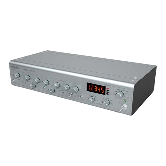
- Page 1 External Cavity Diode Laser Controller DLC102, DLC202, DLC252, DLC502 Revision 9.38...
- Page 2 MOGL Contact For further information, please contact: MOG Laboratories P/L MOGLabs USA LLC MOGLabs Europe 49 University St 419 14th St Goethepark 9 Carlton VIC 3053 Huntingdon PA 16652...
- Page 3 MOGL...
- Page 5 Safety Precautions Safe and effective use of this product is very important. Please read the following safety information before attempting to operate your laser. Also please note several specific and unusual cautionary notes before using the , in addition to the safety precautions MOGL that are standard for any electronic equipment or for laser-related instrumentation.
- Page 6 removed from the controller when it is in the clockwise ( position. • To completely shut off power to the unit, turn the keyswitch anti-clockwise ( position), switch the mains power STANDBY switch at rear of unit to , and unplug the unit. •...
- Page 7 Protection Features includes a number of features to protect you and MOGL your laser. Softstart A time delay (3 s) followed by linearly ramping the diode cur- rent (3 s max). Circuit shutdown Many areas of the circuitry are powered down when not in use. The high voltage supply and piezo drivers, the diode current supplies, the coil driver, and others are without power when the unit is in standby mode, if an interlock is open, or a fault...
- Page 8 Protection relay When the power is off, or if the laser is off, the laser diode is shorted via a normally-closed solid-state relay at the laser head board. Emission indicator The abs controller will illuminate the emission warn- MOGL ing indicator immediately when the laser is switched on.
- Page 9 Extending laser diode and piezo lifetime At night, switch to standby: 1. Switch the laser diode current off. Don’t adjust the current, just switch the toggle up (off). 2. Switch from STANDBY The temperature controller will continue to operate, so the laser is ready for quick startup the next day.
-
Page 10: Table Of Contents
Contents Preface Safety Precautions Protection Features Extending laser diode & piezo lifetime 1 Introduction 1.1 Basic operation ..... . 1.2 Passive frequency control ....locking to an atomic transition . - Page 11 Contents 4 Optimisation 4.1 Frequency reference ....4.2 Noise spectra ..... . . A Specifications response .
- Page 12 Contents H Photodetector H.1 Photodiodes ......Laser head board B1040 headboard ..... B1045/1046 headboard .
-
Page 13: Introduction
TEC voltage C ° e r r e r r l i F r e t r o r Figure 1.1: MOGLabs front panel layout. -
Page 14: Passive Frequency Control
Chapter 1. Introduction STACK 120V SPAN SPAN FREQUENCY TRIG time Figure 1.2: Stack (or current bias) output and trigger pulse, when scan- ning. Note that the ramp slope can be inverted. Details of the ramp behaviour are described in section A.2. 1.2 Passive frequency control controls the laser frequency via the diode current, MOGL... - Page 15 1.2 Passive frequency control Ch1 100mV Ch2 100mV 5.0ms Figure 1.3: A simple absorption spectrum of rubidium with the controller in simple frequency scanning mode. ator ( ) and thus the mid-point frequency of the sweep. As the STACK external cavity frequency changes, the laser may “mode-hop” due to competition between the external cavity and the internal cavity defined by the rear and front facets of the diode saemiconductor chip itself.
-
Page 16: Dc Locking To An Atomic Transition
Chapter 1. Introduction locking to an atomic transition Figure 1.4 shows one possible configuration in which a MOGL is used to lock an to an atomic transition. Locking is to ECDL the side of an absorption peak in a vapour cell; see for example Demtr¨... -
Page 17: Ac Locking To An Atomic Transition
locking to an atomic transition locking to an atomic transition With locking ( demodulation or “lock-in amplifier” detection), the laser frequency can be locked to a peak centre. The proach offers the advantage of inherently lower detected noise and thus the potential for improved laser frequency stability. The setup is similar to that for locking, but modulation of the laser fre- quency, or the reference frequency, is required. - Page 18 Chapter 1. Introduction...
-
Page 19: Connections And Controls
2. Connections and controls 2.1 Front panel controls l o r r e l a t l e r r r r u TEC voltage C ° e r r e r r l i F r e t r o r STANDBY mode, the maintains the laser temperature, but... - Page 20 Chapter 2. Connections and controls CURRENT Diode injection current, 0 to 100/200/250/500 mA (DLC102 to DLC502). The response is not linear; that is, the change in current varies for a given rotation of the knob. The mid-range sensitivity is reduced to allow greater precision at normal operating currents.
- Page 21 2.1 Front panel controls INPUT OFFSET Offset of input light intensity signal, 0 to 10 V. This can be ad- justed to bring the photodetector light signal close to zero on the oscilloscope, and to shift the zero frequency lockpoint for locking.
-
Page 22: Front Panel Display/Monitor
Chapter 2. Connections and controls 2.2 Front panel display/monitor Display selector includes a high-precision 4.5 digit display MOGL with four unit annunciators and 8-channel selector switch. Current * see note below Diode current (mA) Curr max Current limit (mA) ( ) sign indicates limit rather than actual current Voltage Diode voltage (V) ◦... - Page 23 Current feedback [1 V/100 µA] Fast CHAN B Input Photodetector [30 mV/µW] Error Feedback error Current Diode current [2 V full scale*] Modulator output current [1 V/A] ◦ Temp Temperature error [10 V/ * Thus 20, 10, 8, 4 V/A for DLC102/202/252/502.
-
Page 24: Rear Panel Controls And Connections
Chapter 2. Connections and controls 2.3 Rear panel controls and connections l o r r e l o l r a r t a i l : l e r o t a i r IEC power in/out The unit should be preset for the appropriate voltage for your coun- try. - Page 25 2.3 Rear panel controls and connections T gain Temperature control feedback gain. Increase this if the response time is too great or if the temperature error is large. Reduce this if the temperature oscillates. CHANNEL A, B Monitor outputs; connect to oscilloscope, channels 1 and 2. TRIG Oscilloscope trigger, -level.
- Page 26 Chapter 2. Connections and controls Photodetector Connection to photodetector unit. A standard 6-pin FireWire ( IEEE- ) cable is provided. 1394 f sweep Scan rate, 4 – 70 Hz. Note that the rapid return of the sweep STACK drive can excite mechanical oscillations in the laser. Slower sweeps are recommended;...
-
Page 27: Internal Switches And Adjustments
2.4 Internal switches and adjustments 2.4 Internal switches and adjustments See appendix J for schematic overviews of the piezo and diode current control signals, and the effect of the different switches. See appendix L for the location of relevant internal components. CAUTION The cover of the controller should be left on, even loosely, to ensure proper airflow and cooling. - Page 28 Chapter 2. Connections and controls DIP 1, 2 Feedback configuration, see section 2.5. DIP 3 Internal current dither. With , a 250 kHz modulation is DIP 3 ON applied to the injection current, to cause frequency modulation of the laser frequency and generate an error signal for locking (see section 3.5).
- Page 29 2.4 Internal switches and adjustments DIP 9, 13, 14, 15 These switches determine the function of the input on the SWEEP back-panel (see section 3.3 and 3.6). DIP 9 External sweep. Set switch to replace the internal sweep ramp with an external signal.
- Page 30 Chapter 2. Connections and controls the state of SCAN LOCK DIP 15 External slow error. If is on, the external input replaces DIP 15 SWEEP the internally-generated slow (piezo) feedback error signal. The fast (current) feedback path is unaltered, except where overridden ;...
-
Page 31: Feedback Configurations
2.5 Feedback configurations 2.5 Feedback configurations is designed to drive up to three feedback actuators with ap- propriate frequency bandwidths for each. The actuators are STACK . Suitable lasers include the which MOGL DISC CURRENT ECDL feedback but no piezo; DFB/DBR CURRENT STACK DISC... - Page 32 Chapter 2. Connections and controls slow, fast STACK DISC 20 dB/decade, BW 50 Hz STACK 40 dB/decade, BW 1.5 kHz DISC 20 dB/decade, BW 15 kHz CURRENT slow, fast, extra STACK DISC CURRENT 20 dB/decade, BW 50 Hz STACK 40 dB/decade, BW 1.5 kHz DISC 20 dB/decade BW 15 kHz + flat response CURRENT...
- Page 33 2.5 Feedback configurations only CURRENT : fixed STACK : fixed DISC : flat, BW 15 kHz CURRENT 12 should be feedback. DC CURRENT to drive the current with the scanning ramp. For DBR and DFB lasers and ECDLs when it is desirable to operate without piezo actuators.
-
Page 34: Digital Control
Chapter 2. Connections and controls 2.6 Digital control HD12 is a 10-pin header which provides access to several control signals for locking and for sample-and-hold of the lock-point. HD12 is located near the switches, slightly towards the front and left- hand side of the unit (see appendix L). -
Page 35: Internal Trimpots
2.7 Internal trimpots 2.7 Internal trimpots Current dither amplitude limit RT12 Phase lead RT13 Ambient temp for active sensors (AD590, AD592) RT15 current limit locking, either the laser frequency or the external reference must be modulated at the dither frequency, 250 kHz. An external modulator (see appendix G) is normally used, but the laser injection current can be modulated directly. - Page 36 Chapter 2. Connections and controls...
-
Page 37: Operation
3. Operation 3.1 Initial configuration has a wide variety of operating modes. The fol- MOGL lowing describes setting up the temperature and current controllers for regular operation. When purchased with a abs laser, the MOGL will be shipped already correctly configured to operate that laser. -
Page 38: Internal Scan Control
Chapter 3. Operation Curr max display will show a negative sign ( ) as a visual reminder that the limit is being displayed. 7. Switch the laser on. The indicator on the laser head board should illuminate, and the front-panel indicator above the switch should turn green. - Page 39 3.2 Internal scan control Frequency offset (mid-point voltage of the ramp). FREQUENCY Sets the amplitude of the ramp. SPAN Feed-forward bias current adjustment. Can be BIAS adjusted to achieve the widest possible mode- hop free scan range. Disabled unless internal switch f sweep Rear-panel trimpot that adjusts the ramp rate (4...
-
Page 40: External Scan Control
Chapter 3. Operation 3.3 External scan control An external source can be used to control the laser frequency while mode. The control signal should be between 0 and 2.5 V and SCAN must cross 1.25 V to generate the essential internal trigger required for locking. - Page 41 Locking atomic transition. Alternate frequency discriminators, such as a Fabry-Perot cavity, could also be used. A typical schematic for saturated absorption spectroscopy, which is a standard approach to Doppler-free atomic vapour locking, is shown in Figure 3.3. λ/4 λ/4 Vapour cell Offsets ECDL Servo...
- Page 42 Chapter 3. Operation 3. Align the beam(s) onto the photodetector input(s). 4. Find an appropriate spectral feature. 5. Adjust the to eliminate the offset in the photo- INPUT OFFSET diode signal as seen on the signal on INPUT CHAN A 6.
-
Page 43: Ac Locking
Locking Note that it is not necessary to “zoom in” on the desired lock point. The controller will automatically lock to the zero-crossing closest to the trigger point. Locking locking (“top of fringe” locking) is useful for locking the laser directly directly to the peak of an atomic resonance, and is less susceptible to drift than locking. - Page 44 Chapter 3. Operation is near zero. 4. Switch the modulation with the switch. OFF/MOD 5. Find an appropriate spectral peak and observe the dispersive error signal with set to CHAN B ERROR 6. Optimise the error signal (usually for maximum slope) by ad- justing the front panel .
- Page 45 Locking Vapour cell + coil λ/4 f ~ −25mm f ~ 150mm λ/2 250kHz ECDL Servo Lock-in Optical isolator Figure 3.6: Alternative (“retro-reflected”) saturated absorption spec- troscopy configuration. PD is the photodetector. PBS polarising beamsplitter, M mirror, λ/4 and λ/2 are waveplates. 10.
-
Page 46: Locking Using External Signals
Chapter 3. Operation error signal fluctuations, ideally using an external audio spec- trum analyser. The gains should be increased until the onset of oscillation, and then reduced. See chapter 4 for additional discussion. Note that it is not necessary to “zoom in” on the desired lock point. The controller will automatically lock to the zero-crossing of the error signal (in this case the peak of a spectral feature) closest to the trigger point, at the centre of the sweep. - Page 47 3.6 Locking using external signals . If switch , then it should be switched and the will need to be adjusted. BIAS 3. Follow the procedure for locking as appropriate. 3.6.2 External piezo lock (with internal ramp) It is possible to combine the use of the internal ramp with an external control signal, which is useful for combining the front-panel controls with the output of an external PID such as that provided by...
- Page 48 Chapter 3. Operation R113 (5k) R184 R602 R108 R107 R135 R124 R106 R123 R105 R131 R103 R132 R104 Dip Switch Positions 16 ----------------------------- 1 Figure 3.8: R113 is connected so that signals on the rear-panel SWEEP input is always added to the piezo. Remove if using external sweep. mode-hop free scan range of the laser will typically be reduced as compared to using the internal ramp.
- Page 49 3.6 Locking using external signals coupled, and include gain reduction at high frequencies to avoid servo loop oscillation. Note that the external current control signal will only be added to the diode current when is set to SCAN LOCK LOCK For the scenario described in subsection 3.6.3 where SCAN LOCK...
- Page 50 Chapter 3. Operation...
-
Page 51: Optimisation
4. Optimisation Laser frequency stabilisation is a complex and ongoing research topic. A thorough treatment would require extensive discussion of control theory, actuator response, mechanical design, laser-atom in- teractions and electronics. Here we consider the problem from a pragmatic perspective. The laser is assumed to be moderately stable, operating close to the desired frequency, with a linewidth of a few MHz averaged over a typical measurement time of about one second. - Page 52 Chapter 4. Optimisation produce clear (low-noise) dispersive error signals as shown in the upper trace of fig. 3.7. Note that the error signal should be about 0.5 V p-p. While the signal looks cleaner at larger amplitude relative to background oscilloscope noise, in fact the overall performance will deteriorate.
-
Page 53: Noise Spectra
4.2 Noise spectra MOGLabs DLC-202 + ECD-003 monoblock laser noise spectra 1000.00 Unlocked 10.00 Piezo 1.00 Piezo & current 0.10 Off resonance 0.01 Frequency (Hz) Figure 4.1: Error signal spectra, with laser unlocked, locked with SLOW (piezo) feedback only, and with (piezo+current) feedback. - Page 54 Chapter 4. Optimisation onances, outside a Doppler absorption peak. The Off resonance spectrum gives the frequency discriminator noise floor: it is mean- ingless to try to reduce the laser frequency noise below this level. With feedback enabled, the noise for low Fourier frequencies SLOW is drastically reduced.
-
Page 55: A Specifications
A. Specifications Specification Parameter Current regulator 0 to 100/200/250/500 mA Output current 3.2 V at full current; 6 V at half current Max diode voltage /HC models up to 6.5 V at full current ±0 01 mA Display resolution < 10 nA rms (10 Hz – 1 MHz) Noise Warmup time: 15 minutes Stability... - Page 56 Appendix A. Specifications Specification Parameter Piezos 0 to 120 V for (default) FREQUENCY STACK 0 to 150 V optional (LK2 removed) 100 ± 16 4 V feedback DISC 4 to 70 Hz Scan rate Note The default maximum piezo voltage is 120 V but can be increased to 150 V by removing jumper LK2;...
- Page 57 Feedback system 250 kHz, ±8 V, ±500 mA MOD OUT Current output (1 Ω sense) Control via rear-panel trimpot ◦ 0 to 360 (min) PHASE 10 V to +10 V INPUT OFFSET ±0 5 V ERROR OFFSET ±20 dB MASTER ±20 dB GAIN SLOW...
- Page 58 Appendix A. Specifications mains off, or fault condition DARK detected ( failure, polar- ity reversed, open-circuit, ca- ble unplugged, missing sen- sor, temperature out of range) STANDBY RUN LED mains power on Standby ORANGE (temperature controller on) Fully operational GREEN (piezo, current, ramp) Start sequence error or fault (Either...
-
Page 59: Rf Response
response response RBW 30 kHz -30 dBm VBW 10 MHz Ref -20 dBm 50 dB SWT 17 s Center 1.5 GHz 300 MHz/ Span 3 GHz Figure A.1: response, input on laser headboard to diode SMA output. A.2 Sweep saturation and trigger In normal scanning mode, a sawtooth is supplied to the stack piezo (or other laser frequency actuator), at a frequency of 1 to 70 Hz;... - Page 60 Appendix A. Specifications STACK 120V SPAN TRIG time Figure A.2: output voltage and trigger pulse, when STACK FREQUENCY is set near the midpoint (upper) or moved closer to 0 V (lower), where the output voltage exceeds the maximum range.
-
Page 61: B Troubleshooting
B. Troubleshooting detects a wide range of fault conditions and de- MOGL activates related circuitry accordingly. The front-panel provide LEDs indication of the state of these functions. indicator STANDBY Status Colour Temperature controller off. DARK → → Reset via keyswitch, STANDBY Possible faults: •... -
Page 62: Diode Off / On Indicator
Appendix B. Troubleshooting B.2 Diode indicator Status Colour Fault → → Reset via switch Possible faults: • switch not up ( SCAN LOCK SCAN • switch not up ( LOCK • Rear interlock disconnected • Laser head interlock disconnected • Laser head cable disconnected •... -
Page 63: 250 Khz Modulation
B.3 250 kHz modulation B.3 250 kHz modulation The 250 kHz sine-wave oscillator relies on critical non-linear be- haviour of an electronic component. Due to component drift, the oscillator may cease, and the error signal is then lost. A few small adjustments of trimpots will restore the oscillator. - Page 64 Appendix B. Troubleshooting frequency, only. Adjust RT4 first, and once the sine wave appears, adjust RT3 for 250 kHz, then finally adjust RT4 for the 2 6 V p-p. If the oscillator is not stable, try 2.7 V p-p. 3. Probe test point P7 (near RT8 Amp-D and U28), and adjust RT8 to obtain a 1 0 V peak-peak sine wave.
-
Page 65: Locking
B.4 Locking B.4 Locking abs controller provides feedback via three channels each MOGL with a complex servo loop function. A few common problems are addressed here; for more difficult problems, abs will be happy MOGL to work with you to find the best possible solution. B.4.1 does not lock SLOW... - Page 66 Appendix B. Troubleshooting B.4.3 does not lock FAST • feedback has wrong polarity. Try reversing the polarity FAST with the front-panel switch. • If the laser frequency is close to a mode hop (i.e. intrinsic diode cavity resonance is half way between two external-cavity longitudnal modes), the current response can be opposite to normal.
-
Page 67: External Sweep
B.5 External sweep B.5 External sweep Please remember when using external piezo signal ( 9 on), your signal must cross 1.25 V. It can be 1.2 to 1.3 V or 0.5 to 1.5 V but not 1.1 to 1.2 V or 1.5 to 2.0 V. When the signal crosses through 1.25 V, a signal is generated which triggers the control circuits, for example to read the state of the front-panel toggle switches. - Page 68 Appendix B. Troubleshooting...
-
Page 69: C Mode-Hops And Bias
C. Mode-hops and BIAS Mode-hops are a frequent occurrence with external cavity diode lasers. As the laser wavelength is varied, usually by changing the cavity length with a piezo, competition between the frequency de- termined by the different frequency-dependent cavity elements can lead to a mode hop. - Page 70 Appendix C. Mode-hops and BIAS Diode cavity External cavities Diode gain Grating or filter COMBINED 384.0 384.1 384.2 384.3 384.4 Frequency (THz) Figure C.1: Schematic representation for the various frequency-dependent , adapted from Ref. [3], for wavelength λ = 780 nm and factors of an ECDL external cavity length L ext = 15 mm.
- Page 71 C.1 Scanning Adjacent modes -200 -100 Frequency (GHz) Figure C.2: Combined gain for an external cavity diode laser, including the internal and external modes, the diode laser gain, and the filter or grating response. The broad feature is the frequency selectivity of the filter or grating, and the smaller peaks are the external cavity modes (see fig.
- Page 72 Appendix C. Mode-hops and BIAS Figure C.3: Frequency of a laser scanning properly (left) and with a mode- hop at one edge (right). response to adjustment of the temperature setpoint is slow, and you should wait several minutes for the temperature to equilibrate..
- Page 73 C.1 Scanning at least one of these mode hops, then attempt to increase the SPAN further. 12. If the mode hops are at both edges of the scan and cannot be removed by FREQUENCY or CURRENT adjustments, turn the BIAS trimpot either clockwise or counterclockwise to remove one of both of the mode hops.
- Page 74 Appendix C. Mode-hops and BIAS...
-
Page 75: D Using Dbr/Dfb Diodes
D. Using DBR/DFB diodes DBR (Distributed Bragg Reflector) and DFB (Distributed Feed- Back) diodes offer a compact and robust alternative to s. The ECDL linewidth of DBR and DFB diodes is typically 2 to 3 MHz, and they are very susceptible to external optical feedback, necessitating two or even three stages of Faraday isolator to prevent frequency in- stability. -
Page 76: Slow Current Feedback
Appendix D. Using DBR/DFB diodes D.3 Slow current feedback The feedback signal that normally drives the actuator can be DISC coupled to the current feedback, by turning switch 16 ON D.4 Lock saturation Slow drift is normally compensated by the actuator, and hence STACK and current feedback signals only have small range, and... -
Page 77: E Temperature Range
E. Temperature range The default setpoint temperature range of the prod- MOGL ◦ ucts is is 0 C. To change the setpoint range, both the range of the controller and the out-of-limits protection circuit must be changed. Two resistor changes are needed; both are on the top side of the circuitboard. -
Page 78: Setpoint Range (Negative Temperatures)
Appendix E. Temperature range E.2 Setpoint range (negative temperatures) Resistor changes below will change the temperature range to ◦ to +20 C. For other ranges, please contact abs. MOGL R335 from 221k to 43k0. R331 from DNI to 2k0. R315 from 1k00 to 1k20. -
Page 79: F Modulation Coils
Figure F.1: Vapour cell, Zeeman coil, and primary excitation coil, mounted (available from MOGLabs). F.1 Field requirements Ideally the Zeeman dither coil should produce a frequency shift of about half the peak width, typically a few MHz. -
Page 80: Coil Impedance
Appendix F. Modulation coils where is the number of turns per unit length and the current. For wire diameter 0.4 mm, = 2500 m , and the current requirement is only 22 mA/MHz. F.2 Coil impedance However, driving an oscillating current through a coil is problematic because the impedance grows with the frequency. -
Page 81: Impedance Matching
F.3 Impedance matching operates at ω = 250 kHz. For a cell of length MOGL 8 cm, 0.4 mm wire, and 20 mA, we find L Wheeler ≈ 650 µH, and = 20 V, and the maximum slew rate is 32 V/µs. does not have that direct output capability. -
Page 82: Tuning
Appendix F. Modulation coils equals the inductive impedance. That is, ωL = (F.3.7) ωC ω Using the long-solenoid equation for inductance, (F.3.8) ω µ although in practice we find that the inductance is about half the long-solenoid prediction and hence the capacitance should be dou- bled, typically about 1 to 5 nF. -
Page 83: Shielding
F.5 Shielding RBW 1 kHz Marker 1 [T1 ] -30 dBm VBW 30 kHz -41.37 dBm Ref -26 dBm 5 dB SWT 2.5 s 250.000000000 kHz -100 -110 -120 Center 250 kHz 50 kHz/ Span 500 kHz Figure F.3: Coil response acquired using a spectrum analyser with track- ing generator. - Page 84 Appendix F. Modulation coils...
-
Page 85: G External Modulators And Injection Current Modulation
G. External modulators and injection current modulation is designed for locking a laser to an external MOGL reference such as an atomic resonance or an optical cavity. In many cases it is convenient to use the internal modulator driver, and Zee- man modulation of an atomic transition, as described in appendix F. -
Page 86: Injection Current Modulation
Appendix G. External modulators and injection current modulation former. Primary and secondary were wound with 10 turns of PVC- insulated hookup wire around a ferrite bead approximately 15 mm diameter. A 500 Ω potentiometer allows control of the modulation amplitude, and a 9 V battery and 100 kΩ potentiometer provide a shift to set the centre modulator frequency. - Page 87 75 kHz/ Span 750 kHz Figure G.3: beatnote from two MOGLabs -locked lasers. The 3 dB peak width was 750 Hz with a spectrum analyser RBW setting of 300 Hz. For a 20 s average, the width was about 4 kHz.
- Page 88 Appendix G. External modulators and injection current modulation...
-
Page 89: H Photodetector
A number of M4 and 8-32 threaded holes allow mounting in differ- ent configurations to minimise the footprint on an optical bench (see figure H.2). Figure H.1: MOGLabs balanced differential photodetector. Figure H.2: M4 mounting holes are marked with a dimple; others are... -
Page 90: Photodiodes
Appendix H. Photodetector H.1 Photodiodes The standard photodetector uses Si-PIN photodiodes encapsulated in a coloured plastic which transmits in the near-infrared and blocks most room light. The diodes include a lens to reduce the acceptance ◦ angle to ±10 . Unfiltered diodes, and wider acceptance angles, are also available. -
Page 91: I Laser Head Board
I. Laser head board The laser head interface board provides connection breakout to the laser diode, , sensor, piezo actuators, and laser head interlock. It also includes a protection relay and passive protection filters, a laser-on indicator, and an connection for direct diode current modulation. -
Page 92: B1040 Headboard
MOLEX does not provide a mechanism for optical power MOGL control or measurement for diodes with an internal photodiode. Figure I.1: MOGLabs laser head board showing headers for con- nection of laser diode, piezo actuators, temperature sensor, and head enclosure interlock. Connectors are Molex KK-100. -
Page 93: B1045/1046 Headboard
(see I.2.1 below). Figure I.2: MOGLabs B1045 and B1046 laser head boards showing con- nectors for laser diode, piezo actuator, temperature sensors, and head enclosure interlock. Connectors are Hirose DF59. - Page 94 Appendix I. Laser head board between the head board and the diode. The input impedance is 10 k. The sensitivity depends on the diode impedance but is typically around 1 mA/V. WARNING: The input is a direct connection to the laser diode. Excessive power can destroy the diode, which is separated from the head board relay by an inductor.
-
Page 95: B1047/B1240 Headboards
I.3 B1047/B1240 headboards I.3 B1047/B1240 headboards The B1047 and B1240 provide high-speed active modulation of the diode current. They use 500 MHz opamps and very low latency circuitry to reduce phase delay to around 12 ns for the B1240. The B1047 allows for closed-loop bandwidth of about 1.2 MHz while the B1240 can achieve about 4 MHz (in both cases, without phase advance). - Page 96 Appendix I. Laser head board I.3.1 input The B1047/B1240 input provides coupling to an active modulation circuit. Note that connection to the input will reduce the diode current by about 1.6 mA (B1047) to 2.5 mA (B1240), with zero input voltage. B1047 B1240 ±2 0 V max...
-
Page 97: Headboard Connection To Controller
I.4 Headboard connection to controller I.4 Headboard connection to controller Note (dual link) cable. abs laser cable is a digital MOGL DVI-D DL There is a bewildering assortment of apparently similar cables avail- able. Most computer display cables will not work because they are missing important pins;... -
Page 98: Dual Piezo Operation
Appendix I. Laser head board I.5 Dual piezo operation provides outputs to two piezo elements. They can be con- figured as: Single Typically, only a single “stack” actuator, such as the Tokin (available from Thorlabs, www.thorlabs.com), will AE0203D04 be required. The single stack actuator allows frequency scan- ning and frequency offset selection, and active slow feedback (up to ≈... - Page 99 Cover interlock (option) s i s Figure I.6: MOGLabs laser head board schematic (B1040/1045). The modulation low-pass cutoff frequency is determined by C4 and the diode impedance (∼ 50Ω).
- Page 100 Appendix I. Laser head board...
-
Page 101: Control Overview
J. Control overview Front panel MOD Dip 3 Current dither enable Dither on/o Sine ref 250kHz Rear panel I mod Diode current Dither current Gain dither RT6 current Front panel dither gain PHASE Phase 0 − 360° Mod out Demodulator Sine ref Test Front panel... - Page 102 Appendix J. Control overview Rear panel Sweep frequency (f sweep ) Dip 9 External sweep enable Sweep generator Summer Rear panel BNC Front panel or DI-2 Bu er R113 SWEEP/PZT MOD Scan/Lock Rear panel BNC Front Panel TRIG External Span sweep signal Sweep amplitude trigger out (TTL)
- Page 103 Dip 12 RT12 Front Panel Bypass AC Phase gain Current gain 100uA/V Error signal Integrator Phase lead Sum/gain 2.5mA/V Phase midpoint polarity control Front panel or DI-3 Front panel Current control Current enable ‘FAST’ polarity Bu er Dip 6 External Rear panel - BNC current enable External Signal...
- Page 104 Appendix J. Control overview...
-
Page 105: K Connectors And Cables
K. Connectors and cables K.1 LASER WARNING connector should only be connected to a abs laser LASER MOGL or laser head board. High voltages are present on some pins. The supplies will be disabled if the cable is disconnected, but never- theless considerable care should be taken to ensure non- MOGL devices are not connected. -
Page 106: Photodetector
Appendix K. Connectors and cables A 10 k thermistor should be connected to NTC+ and NTC–, but an AD590 or AD592 temperature sensor can be instead be connected to T . Pin 15 provides +5 V. Relay GND (pin 14) is grounded sense when the laser diode is activated, to open the relay that otherwise short-circuits the laser diode. -
Page 107: Digital Control
K.4 Digital control +5V/5k LASER ø6.5mm ENABLE ø2.1mm Figure K.3: INTERLOCK connector on rear panel. K.4 Digital control HD12 is a 10-pin header which provides access to several impor- tant control signals for locking and for sample-and-hold of the lock- point, as described in section 2.6. - Page 108 Appendix K. Connectors and cables...
-
Page 109: L Pcb Layout
L. PCB layout... - Page 110 Appendix L. PCB layout...
-
Page 111: M 115/230 V Conversion
M. 115/230 V conversion M.1 Fuse The fuse is a ceramic antisurge, 2.5A, 5x20mm, for example Littlefuse 021502.5MXP. The fuse holder is a red cartridge just above the IEC power inlet and main switch on the rear of the unit (Fig. M.1). Figure M.1: Fuse catridge, showing fuse placement for operation at 230 Vac. - Page 112 Appendix M. 115/230 V conversion Figure M.2: To change fuse or voltage, open the fuse cartridge cover with a screwdriver inserted into a small slot at the top of the cover, just above the red voltage indicator. When removing the fuse catridge, insert a screwdriver into the recess at the top of the cartridge;...
- Page 113 M.2 120/240 V conversion Figure M.4: Bridge (left) and fuse (right) for 230 V. Swap the bridge and fuse when changing voltage, so that the fuse remains on the right-hand side (see below). Figure M.5: Bridge (left) and fuse (right) for 115 V.
- Page 114 Appendix M. 115/230 V conversion...
-
Page 115: References
Bibliography [1] C. J. Hawthorn, K. P. Weber, and R. E. Scholten. Littrow config- uration tunable external cavity diode laser with fixed direction output beam. Rev. Sci. Inst., 72(2):4477, 2001. i [2] L. Ricci, M. Weidem¨ u ller, T. Esslinger, A. Hemmerich, C. Zimmer- mann, V. - Page 118 2007 – 2018 MOG Laboratories Pty Ltd 49 University St, Carlton VIC 3053, Australia Product specifications and descriptions in this doc- Tel: +61 3 9939 0677 info@moglabs.com ument are subject to change without notice.
Need help?
Do you have a question about the DLC102 and is the answer not in the manual?
Questions and answers