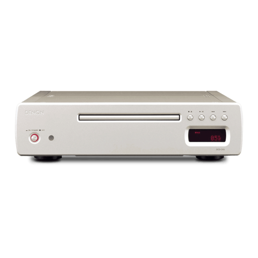
Denon DCD-CX3 Service Manual
Super audio cd player
Hide thumbs
Also See for DCD-CX3:
- Owner's manual (23 pages) ,
- Operating instructions manual (19 pages) ,
- Dimensions (1 page)
Table of Contents
Advertisement
Quick Links
MODEL
DCD-CX3
For purposes of improvement, specifications and
●
design are subject to change without notice.
Please use this service manual with referring to the
●
operating instructions without fail.
Some illustrations using in this service manual are
●
slightly different from the actual set.
SERVICE MANUAL
JP
SUPER AUDIO CD PLAYER
サービスをおこなう前に、このサービスマニュアルを
必ずお読みください。本機は、火災、感電、けがなど
に対する安全性を確保するために、さまざまな配慮を
おこなっており、また法的には「電気用品安全法」に
もとづき、所定の許可を得て製造されております。
従ってサービスをおこなう際は、これらの安全性が維
持されるよう、このサービスマニュアルに記載されて
いる注意事項を必ずお守りください。
e
Denon Brand Company, D&M Holdings lnc.
E3
E2
EK
g
注 意
本機の仕様は性能改良のため、予告なく変更すること
●
があります。
補修用性能部品の保有期間は、製造打切後 8 年です。
●
修理の際は、必ず取扱説明書を参照の上、作業を行っ
●
てください。
本文中に使用しているイラストは、説明の都合上現物
●
と多少異なる場合があります。
Ver. 5
Please refer to the
MODIFICATION NOTICE.
E2A E1C E1K EUT
S-1184 V.05 DE/CDM 0803
Advertisement
Table of Contents

Subscribe to Our Youtube Channel
Related Manuals for Denon DCD-CX3


Summary of Contents for Denon DCD-CX3
- Page 1 Please use this service manual with referring to the ● 修理の際は、必ず取扱説明書を参照の上、作業を行っ ● operating instructions without fail. てください。 Some illustrations using in this service manual are ● 本文中に使用しているイラストは、説明の都合上現物 ● slightly different from the actual set. と多少異なる場合があります。 Denon Brand Company, D&M Holdings lnc. S-1184 V.05 DE/CDM 0803...
-
Page 2: Safety Precautions
DCD-CX3... - Page 3 ◎指定部品の使用! 定格(定格電力、耐圧)を持ったものを使用しても安全性 セットの部品は難燃性や耐電圧など安全上の特性を持っ が維持されるとは、 限りません。 安全上の特性を持った部 たものとなっています。 従って交換部品は、 使用されてい 品は、 このサービスマニュアルの配線図、 部品表につぎの たものと同じ特性の部品を使用してください。特に配線 ように表示していますので必ず指定されている部品番号 図、部品表に z 印で指定されている安全上重要な部品は のものを使用願います。 必ず指定のものをご使用ください。 (1) 配線図… z マークで表示しています。 ◎部品の取付けや配線の引きまわしは、 (2) 部品表… z マークで表示しています。 元どおりに! 指定された部品と異なるものを使用した場 安全上、テープやチューブなどの絶縁材料を使用したり、 合には、感電、火災などの危険を生じる恐 プリント基板から浮かして取付けた部品があります。 また れがあります。 内部配線は引きまわしやクランパーによって発熱部品や 高圧部品に接近しないように配慮されていますので、 これ らは必ず元どおりにしてください。 DCD-CX3...
- Page 4 1. Top Panel and Side Panel 1. トップパネル、サイドパネルのはずしかた (1) Remove 8 top screws, then detach Top Panel. (1) トップパネルを取り付けているネジ 8 本をはずしま す。 (2) Remove 4 side screws, then detach Side Panel. (2) トップパネルを矢印の方向にはずします。 (3) サイドパネルを取り付けているネジ 4 本をはずしま す。 (4) サイドパネルを矢印の方向にはずします。 DCD-CX3...
- Page 5 (3) Remove 3 top screws and bottom 3 screws, then de- (3) フロントパネルを取り付けている、 上部のネジ 3 本と tach the Front Panel Ass’y. 底部のネジ 3 本をはずします。 (4) フロントパネルを矢印の方向にはずします。 ※ If front panel is abandoned, disassemble according to ※ フロントパネルを廃棄する場合は、下図のように分解し below. てください。 DCD-CX3...
- Page 6 (1) フロントアングルを取り付けているネジ2本をはずし ます。 (2) フロントアングルを矢印の方向にはずします。 (2) Remove 2 Mecha Bracket screws, then detach SACD (3) メカブラケットを取り付けているネジ 2 本をはずしま Mechanism. す。 (4) SACD メカを矢印の方向にはずします。 ※ If SACD Mechanism is abandoned, disassembles ※ SACD メカを廃棄する場合は、メカ分解図のように分解 してください。 according to Mechanism exploded view. DCD-CX3...
-
Page 7: Front Panel
(2) フロントアングルを取り付け、ネジ 2 本を締めます。 (3) 6 screws of Front Panel are tightened. (3) フロントパネルを取り付け、ネジ 6 本を締めます。 ※ Loader Panel is the parts to which a scratch tends to ※ ローダーパネルにキズを付けないよう、注意してく be attached. Be fully careful in the case of work. ださい。 DCD-CX3... - Page 8 Front Panel. (Refer to Fig. A) す。 (fig. A 参照) (4) 2 screws are tightened. (Refer to Fig. B) (4) ネジ 2 本を締めます。 (fig.B 参照) fig. B MECHA BRACKET MECHA HOLDER fig. A DCD-CX3...
- Page 9 (1) 4 screws are tightened forcing Side Panel in the direc- 締めます。 tion of an arrow. 4. Top Panel 4. トップパネルの取り付け (1) 8 screws of Top Panel are tightened, forcing Side Pan- (1) サイドパネルとトップパネルを矢印の方向に同時に el and Top Panel simultaneously to the direction of the 押しながら、トップパネルのネジ 8 本を締めます。 arrow. DCD-CX3...
- Page 10 レーザー駆動電流 Iop 値の確認 HF wave form check HF 波形の確認 (Refer to WAVE FORMS) (WAVE FORMS 参照) Present value exceeds the ini- 現在値が初期値の tial value by 1.5 times 1.5 倍になっている Traverse Unit replacing トラバースユニット交換 Laser current (Iop) memorizing after replacement 交換後にレーザー電流値の記憶 DCD-CX3...
- Page 11 (Traverse Unit) ト ) の交換 Check the Iop (Laser drive current) Iop( レーザー駆動電流)をチェックします。 If the present Iop (current) value exceeds.+150% of the 現在の Iop 値が初期値の 150%を越えている場合、トラ initial value, replace the Traverse unit (Laser Pick-up) with バースユニット(レーザーピックアップ)を交換してく a new one. ださい。 DCD-CX3...
- Page 12 FL 管の表示 (8 桁の表示部 ) FL Display (The display part of 8 digits) T 2 ― ― T 2 ― ― ボタンを押すと、 "T21" 現在値を保存せず、 "T22" (5) Press the button to display the current value 現在値の表示へ戻ります。 “T22” without storing the current value “T21”. DCD-CX3...
- Page 13 "nnnnn" is displayed as 0 so you can check. FL 管の表示 (8 桁の表示部 ) FL Display (The display part of 8 digits) T T ( −:消灯、Y:1: CD, 2: DVD、nnnnn:時間 [h]) ( − : Off, Y:1: CD, 2: DVD, nnnnn: Hour [h]) DCD-CX3...
- Page 14 Spring at this time. (Spring り付け用突起を押さないようにします。 (スプリング may be warped) が変形する可能性が高いため) SLIDE CAM side (3) Check that the projection of Mecha Frame becomes (3) トレイ左側に設けられた孔より、メカフレームの突 position of the photograph, from the hole at the left on 起部が写真に示す位置になっていることを確認しま the Tray. す。 DCD-CX3...
- Page 15 (2) Remove 4 screws then detach SACD MODULE (2) SACD MODULE 基板を固定しているネジ 4 本をはず P.W.B. し、基板をはずします。 (3) Remove 4 screws fixing DAMPER. (3) ダンパーを固定しているネジ 4 本はずします。 (4) Remove Traverse Unit in the arrow direction. (4) トラバースユニットを矢印方向にとりはずします。 7P PH 6P PH 15P FFC 24P FFC DCD-CX3...
- Page 16 CD TEST MODE & SERVICE MODE DCD-CX3...
- Page 17 (7) レーザー ON 累積時間表示モード : TB (8) Monitor terminal setting mode : TD (8) モニタ端子設定モード : TD (9) SACD watermark signal quality checking mode : TE (9) SACD ウォーターマーク信号品質確認モード : TE (10) Self test mode : TF (10) 自己診断モード : TF DCD-CX3...
- Page 18 FL Display (The display part of 8 digits) T 7 T 7 FL 管の表示 (8 桁の表示部 ) FL Display (The display part of 8 digits) T 3 T 3 FL 管の表示 (8 桁の表示部 ) FL Display (The display part of 8 digits) T 2 T 2 DCD-CX3...
- Page 19 X = 5 :レーザー OFF X = 5 : The laser off mm.mm :保存値 [mA] ( 保存データなしの場合は消灯 ) mm.mm : Stored value [mA] ( If stored value is not, “mmmm” turns off. ) nn.nn :現在値 [mA] nn.nn : Current value [mA] DCD-CX3...
- Page 20 ボタンで確定します。 各サーボ調整値が表示されます。 FL Display (The display part of 8 digits) FL 管の表示 (8 桁の表示部 ) T T n n n n : Selection mode XXX : 選択モード nnnn : Adjustment value (HEX, 2Byte) nnnn : 調整値 ( 16進数、2バイト ) DCD-CX3...
- Page 21 ボタンを押し "TB3" When TB1 or TB2 is selected with the button, "nnnnn" is displayed as 0 so you can check. を表示させます。"TB3" 表示後に ボタンを押すと、CD 及び DVD レーザー ON 累積時間をクリアします。 または ボタンで "TB1" または "TB2 " を選択すると、" nnnnn" 部が "0 " 表示となり確認できます。 DCD-CX3...
- Page 22 = 2 : Monitor setting ( Addr = 0x38, Data = 0x06 setting ) : モニタ設定 ( Addr =0x3 8, Data = 0x06 設定 ) MNIT2 terminal : Sector Detect Error MNIT2 端子:Sector Detect Error MNIT1 terminal : PDM Detect MNIT1 端子:PDM Detect MNIT0 terminal : PSP-DATA OK MNIT0 端子:PSP-DATA OK DCD-CX3...
- Page 23 OPEN 表示 (It readjusts with heat run mode.) ↓ OPEN display CLOSE 表示 ↓ ↓ CLOSE display READING 表示 ↓ ↓ READING display FL 管の表示 (8 桁の表示部 ) ↓ FL Display (The display part of 8 digits) T T DCD-CX3...
- Page 24 L0 層 TE 信号の AGC 値 (0x100 で 1 倍、0x200 で 2 倍。 Y/0x100 の比率計算) teagc0 L0 layer TE signal AGC value (1x for 0x100, 2x for 0x200. Y/0x100 ratio calculation.) TE の振幅が目標ターゲット 2.45V になる様に調整される。 Adjusted so that TE amplitude reaches target of 2.45V. DCD-CX3...
- Page 25 L1 layer AS signal AGC value (1x for 0x100, 2x for 0x200. Y/0x100 ratio calculation.) asagc1 L1 層 AS 信号の AGC 値 (0x100 で 1 倍、0x200 で 2 倍。 Y/0x100 の比率計算) Adjusted so that AS amplitude reaches target of 2.45V. AS の振幅が目標ターゲット 2.45V になる様調整される。 DCD-CX3...
- Page 26 HYBR DVD-VR DVvr SACD(Hybrid) HYBR DVD-VR DVvr Unknown NONE Mixed mode CD-ROM CDRD 不明 NONE Mixed mode CD-ROM CDRD SACD SACD SACD SACD (When there are multiple formats, the format played and identified with priority is displayed.) ( フォーマットが混在する場合、優先して再生、認識されるフォーマットを表示します。) DCD-CX3...
- Page 27 A display of PI uncorrectable number of the outer circumference of In the case of 1-layer DVD disc, it is invalid. 2 層外周の PI 訂正不可数とアドレスの表示 DVD 1 層ディスクの場合、無効。 2-layer and an address. CD : C2 uncorrectable error number (x6) CD 時は C2 訂正不可数。(x6) DCD-CX3...
-
Page 28: Trouble Shooting
1.2V DC (switched) Voltage is O.K.? and Other Circuits (1U-3788, C124 + Terminal) O.K. Check +2.5V Output Check Parts and Soldering. • Voltage Check N.G. • [IC503] (BA25BC0FP) 2.5V DC (switched) Voltage is O.K.? and Other Circuits (1U-3788, C543 + Terminal) DCD-CX3... - Page 29 O.K. ・ [IC110] (BA33BC0FP) ・ (C139 + 端子 ) その他この出力の負荷となる回路 Check +3.3V Output Check Parts and Soldering. • Voltage Check O.K. N.G. • [IC110] (BA33BC0FP) 3.3V DC (switched) Voltage is O.K.? and Other Circuits (C139 + Terminal) 終了 O.K. DCD-CX3...
- Page 30 ・ [RST]: "H" level? (2) FL601 の半田付けを確認 • [RST]: "H" level? (2) Check Soldering of FL601 ・ テストモード T0 実行 全点灯 OK? • The test mode "T0" is executed. The FL tube display turns all on? O.K. O.K. 終了 DCD-CX3...
- Page 31 • Check the voltage of Test-Point (TP)) 1U-3788(SACD MODULE UNIT) ・ テストポイント (TP) の電圧確認 ・ [IC157] とその周辺の半田付けを確認 • TP[mAMON1] [AMON2]: differential output about • Check the circumference soldering of [IC157] ・ TP [AMON1] [AMON2]: 差動出力 約 700mVp-p 700mVp-p O.K. O.K. 終了 DCD-CX3...
- Page 32 • [IC502]: 1, 23, 117-120, 111-114pin ・ [IC502]: 1, 23, 117-120, 111-114pin "H" ⇔ "L" alternate? "H" ⇔ "L" 切替 R539, R543-551 R539, R543-551 • The test mode "TE" is executed. 190 over? ・ テストモード TE 実行 190 以上? O.K. O.K. 終了 DCD-CX3...
- Page 33 (5)GND_DISP (8)KEY0 (6)+32V 1U-3789-7 (6)+32V <FL Display (9)FDAT (7)F+ LED UNIT (7)F+ (1)RED_LED (10)FCLK (8)F− built in FL Driver> (8)F− (11)FCS (2)GND_DISP RED LED (12)FRST (3)ORG_LED 1U-3789-6 ORG LED CX033 (13)GND_D1 1U-3789-4 DISPLAY UNIT REMOCON UNIT 3P-PH CY033 3P-PH DCD-CX3...
- Page 34 ---MEMO--- DCD-CX3...
- Page 35 External memory address 9 / data 11 EXADT8 EXT ADR8 External memory address 8 / data 4 VDD33 3.3V I/O supply EXADR19 EXT ADR19 External memory address 19 NEXWE EXT WE External memory write enable EXADR183 EXT ADR18 External memory address 18 DCD-CX3...
- Page 36 RF input 2 VIN4RF VIN4RF RF input 4 VIN3RF VIN3RF RF input 3 AVDDB 3.3V Analog supply VREFH5 V-REF-H5 5 bit AD reference Voltage "H" VREFL5 V-REF-L5 5 bit AD reference Voltage "L" AVSSB Analog GND LPC1 LPC1 DVD LPC input DCD-CX3...
- Page 37 VDIOO IO_RST RST for CXD2753 VDD33 3.3V I/O supply EXTRG1 OPEN Video clock output SCLOCK SCLOCK Input clock for debug SDATA SDATA Input/output data for debug EXTRGO PDETECT/EXTRGO System ucom port 41 TRCCLK CLK33M Master clock for External AVDEC DCD-CX3...
- Page 38 SDRAM data mask 2 DQM3 SDRAM DATA MASK3 SDRAM data mask 3 MDQ31 SDRAM DATA31 SDRAM data 31 MDQ16 SDRAM DATA16 SDRAM data 16 MDQ30 SDRAM DATA30 SDRAM data 30 MDQ17 SDRAM DATA17 SDRAM data 17 MDQ29 SDRAM DATA29 SDRAM data 29 DCD-CX3...
- Page 39 I/O(A11) I/O(B11) MODE I/O(A12) IN_INV I/O(B12) IN_B12 I/O(A13) I/O(B13) IN_B13 I/O(A14) I/O(B14) AND_02 I/O(A15) I/O(B15) Pure Direct CLK1/I CLK1/I CLK3/I CLK3/I CLK2/I CLK2/I CLK0/I CLK0/I I/O(B0) I/O(A0)/GOE0 I/O(B1) SCK(1796) I/O(A1) SCK(2753) I/O(B2) I/O(A2) I/O(B3) 64fs(1796) I/O(A3) 64fs(2753) I/O(B4) I/O(A4) DCD-CX3...
- Page 40 NRST for DV3.2 P15(INT3) DV_STB ON/STB OK from DV3.2 P14(PPG) REDLED RED LED H;ON (for POWER ON) P13(DVO) ORGLED ORG LED H;ON (for STANDBY) OPEN P12(INT2/TC1) OPEN P11(INT1) OPEN P10(PDO3/PWM3/TC3) REMO_SEL REMOTE LINE SELECT (L;DV3.2 H;STANDBY(TMP86)) P30(AIN0) OPEN P31(AIN1) OPEN DCD-CX3...
- Page 41 V COM L Oversampling Advanced PDATA Digital Bias I REF Segment Filter V COM R Vref Modulator Function Control I OUT R– Function Control Current V OUT R Segment I OUT R+ I/V and Filter System Clock Manager Power Supply DCD-CX3...
- Page 42 BA33BC0FP (IC110, 806) BLOCK DIAGRAM GND(FIN) Vref Pin No. Pin Name Driver N.C. Vcc (1PIN) N. C. (2PIN) OUT (3PIN) PQ033RDA2SZH (IC807) : DC input (V in) : DC output (V o) : GND : ON/OFF control (V c) DCD-CX3...
- Page 43 2. FL DISPLAY 8-BT-258GINK (FL601) PIN CONNECTION ANODE CONNECTION PIN CONNECTION SEGMENT DESIGNATION DCD-CX3...
- Page 44 ---MEMO--- DCD-CX3...
- Page 45 PRINTED WIRING BOARDS 1U-3788 SACD MODULE P.W.B. UNIT COMPONENT SIDE FOIL SIDE DCD-CX3...
- Page 46 1U-3789 AUDIO/POWER/DSP P.W.B. UNIT COMPONENT SIDE DCD-CX3...
- Page 47 FOIL SIDE DCD-CX3...
- Page 48 1U-3791 FGCX P.W.B. UNIT COMPONENT SIDE FOIL SIDE COMPONENT SIDE COMPONENT SIDE FOIL SIDE FOIL SIDE COMPONENT SIDE DCD-CX3...
-
Page 49: Note For Parts List
Indicates number of zeros after effective number. 2-digit effective number. Units: pF. 220pF (0 or 1) Indicates number of zeros after effective number. 2-digit effective number. Units: pF. When the dielectric strength is indicated in AC, "AC" is included after the dieelectric strength value. DCD-CX3... - Page 50 00D 272 0166 905 2SB798(DL/DK)-T1 +C TR118 00D 273 0487 904 2SC2412K_T146R TR119 00D 274 0204 902 2SD999(CM/CL)-T1 +C TR120 00D 272 0166 905 2SB798(DL/DK)-T1 +C D103,104 00D 276 0717 903 1SS355 TE-17 D501 00D 276 0717 903 1SS355 TE-17 DCD-CX3...
- Page 51 00D 257 0520 911 CK73B1A224KT +1608 C174 00D 257 0516 954 CK73B1E104KT +1608 C176 00D 257 0516 954 CK73B1E104KT +1608 C177,178 00D 257 0506 951 CC73CH1H101JT +1608 C179 00D 257 0509 929 CK73B1H102KT +1608 C180 00D 257 0501 901 CK73B1H103KT (1608) +1608 DCD-CX3...
- Page 52 +1608 C510 00D 257 4011 905 CE67C0J101MT (RV2) +REF C511 00D 257 0516 954 CK73B1E104KT +1608 C512,513 00D 257 0501 901 CK73B1H103KT (1608) +1608 C514 00D 257 0516 954 CK73B1E104KT +1608 C515 00D 257 0501 901 CK73B1H103KT (1608) +1608 DCD-CX3...
- Page 53 +1608 C602 00D 257 4011 905 CE67C0J101MT (RV2) +REF C603,604 00D 257 0516 954 CK73B1E104KT +1608 C605 00D 257 0501 901 CK73B1H103KT (1608) +1608 C607 00D 257 0516 954 CK73B1E104KT +1608 C608 00D 257 0501 901 CK73B1H103KT (1608) +1608 DCD-CX3...
- Page 54 00D 235 0130 903 CHIP EMIFIL(11A121) +1608 FB501-507 00D 235 0130 903 CHIP EMIFIL(11A121) +1608 FB508 00D 235 0136 907 FBMJ1608HS280NT +1608 L101-103 00D 235 0125 905 INDUCTOR(FLC32C220K)+3216 X101 00D 399 0619 906 XTAL(27MHZ) +REF X102 00D 399 0801 905 CSTCE8M00G52-RO DCD-CX3...
- Page 55 D827 00D 276 0717 903 1SS355 TE-17 D828-831 00D 276 0751 901 1SR154-400TE25 +REF ZD801 00D 276 0624 902 MTZJ2.0A T77 ZD802,803 00D 276 0683 998 UDZS16B-TE17 ZD804 00D 276 0798 922 UDZS18B-TE17 LD701 00D 393 9667 003 SLA-360LT3F(XE) DCD-CX3...
- Page 56 00D 254 4694 909 CE04W1E101MT(RF0) C155 00D 255 4256 955 CQ93P2A103JT(NH2) C156 00D 255 1265 936 CQ93M1H103JT(B) C157 00D 257 0501 901 CK73B1H103KT (1608) +1608 for E2 C158 00D 257 0516 954 CK73B1E104KT +1608 for E2 C162 00D 255 4256 955 CQ93P2A103JT(NH2) DCD-CX3...
- Page 57 CK73B1E104KT +1608 C617 00D 257 0501 901 CK73B1H103KT (1608) +1608 C801 00D 254 4573 981 CE04W1H100MT(RA3) C809 00D 257 0501 901 CK73B1H103KT (1608) +1608 C815 00D 257 0516 954 CK73B1E104KT +1608 C816 00D 257 0501 901 CK73B1H103KT (1608) +1608 DCD-CX3...
- Page 58 2P VH CONNECTOR BASE CX023 00D 205 0581 069 2P VH CON BASE (Red) CX024 00D 205 0581 001 2P VH CON BASE (White) CX031 00D 205 0343 032 3P CONN.BASE(KR-PH) CX032 00D 205 0233 032 3P EH CONNECTOR BASE DCD-CX3...
- Page 59 101 010 0180 00D POWER TRANS(MINI E3) for E3 X101 00D 399 1043 908 C70315-33.8688-15-3.3V AS807 RADIATOR AS808 RADIATOR 0RD 471 3304 015 3X8 CBS-Z 00D 203 0386 093 1P SIN CON ASS'Y W306-W310 00D 415 0866 006 CONDENSER COVER C864,865 DCD-CX3...
- Page 60 00D 205 0343 032 3P CONN.BASE(KR-PH) CX033 00D 205 0343 032 3P CONN.BASE(KR-PH) CX061 00D 205 0343 061 6P CONN.BASE(KR-PH) CX071 00D 205 0343 074 7P CONN.BASE(KR-PH) CY051 00D 205 0343 058 5P CONN.BASE(KR-PH) S101 00D 212 1206 008 SPVF130100 DCD-CX3...
- Page 61 ---MEMO--- DCD-CX3...
- Page 62 EXPLODED VIEW sg 152 162 JP only 158 168 153 163 151 161 155 165 156 166 WARNING: Parts marked with this symbol have critical characteristics. Use ONLY replacement parts recommended by 154 164 the manufacturer. 印の部分は安全を維持するために重要 155 165 な部品です。従って交換時は必ず指定の 部品を使用してください。 DCD-CX3...
- Page 63 SIDE BRACKET for E2, E3 00D 461 1253 019 RUBBER SHEET for E2, E3 0RD 445 0048 016 CORD HOLDER (L50) 00D 412 2741 036 P.W.B.HOLDER (H=10) 00D 412 2814 028 CARD SPACER(L=10) 00D 445 0067 013 CORD KEEP DCD-CX3...
- Page 64 JP 0RD 473 7505 007 2.6X8 CBTS (P)-Z 0RD 471 2000 006 2X3 CFS-NI 00D 477 0064 107 FIXING SCREW 0RD 473 7015 005 3X6 CBTS(S)-B 0RD 471 3004 001 3X5 CBS -B 0RD 471 9058 022 SPECIAL SCREW DCD-CX3...
- Page 65 00D 125 0075 004 CHUKOH TAPE(W25/T0.13) for JP L=30 < EMI GASKET > Ref. No. Part No. Part Name Remarks Q'ty 00D 461 1209 005 EMI G.(SHSG050100) for E2 L=80 00D 461 1209 005 EMI G.(SHSG050100) for E2 L=20 DCD-CX3...
- Page 66 ---MEMO--- DCD-CX3...
- Page 67 EXPLODED VIEW OF SACD MECHANISM WARNING: Parts marked with this symbol have critical characteristics. Use ONLY replacement parts recommended by the manufacturer. 印の部分は安全を維持するために重要 な部品です。従って交換時は必ず指定の 部品を使用してください。 DCD-CX3...
- Page 68 Both ends side of boss contact CAM SPRING attachment area (0.9mg) area under BECA BASE-SLIDE CAM. (7.0mg each x 2) Grease : EM30L Only shaft area of gear axis (2.0mg each x 2) TRAY bottom MECHA BASE Greasing positions MECHA BASE bottom DCD-CX3...
- Page 69 SLIT WASHER 1.7x3.2x0.5 00D 475 1157 091 SLIT WASHER 3.1x5.4x0.5 00D 475 1190 003 SLIT WASHER 3.1x12.0x0.5 00D 475 1161 016 POLY WASHER 4.1x6.5x0.5 00D 476 1003 009 3E RING 2x6CBTS(P)-Z 00D 9KC 1H01 1 SCR-DAMPER 00D 9KC 2G08 3 DAMPER-IDLE DCD-CX3...
- Page 70 CORD HOLDER WIRE CLAMP BAND 100mm WIRE CLAMP BAND 160mm 3x5CFS-B 00D 415 0716 020 SUMI TUBE 00D 461 1286 002 SHAFT SPACER 00D 009 0276 019 24P FFC(0.5) L90 MECHA BRACKET 3x6CPS(SW.W)ZNP 00D1U-3788 SACD MODULE UNIT 3X6 CBTS(S)-Z DCD-CX3...
- Page 71 00D 998 0011 205 POS LABEL for JP UPC LABEL for E3 00D 513 9111 030 COLOR LABEL for E2, E3 CONT.CARD(L)SUB ASSY for E2, E3 00D 502 1139 007 PAD(AC CORD) for E2, E3 00D 515 0944 707 WARRANTY(HOME) for E3 DCD-CX3...
- Page 72 さい。 1U-3788 SAD MODULE P.W.B. Unit : Component Side * Reference voltage of ⑬ , ⑯ ~ is GND_D1 ⑮ , and reference voltage of other point is VC16 ⑭ . *⑬、⑯∼ の基準電圧は GND_D1 ⑮で、他のポイントの基準電圧は VC16 ⑭です。 DCD-CX3...
- Page 73 GND ; VC16 SACD Play (INNER) CD Play (INNER) SPINDLE SPINDLE GND ; VC16 GND ; VC16 SACD Search (INNER→OUTER) CD Search (INNER→OUTER) SLED SLED SLED + SLED + SLED - SLED - GND ; VC16 GND ; VC16 DCD-CX3...
- Page 74 LODEAR OPEN / COLSE OPEN CLOS LOAD+ CX071(6) FL_LIM_SENS CX071(2) FL_LIM_SW CX071(3) RE_LIM_SENS CX071(4) CHACKING UP / DOWN DOWN CHA+ CX061(2) UP_SW CX061(5) DOWN_SW CX061(4) DCD-CX3...
- Page 75 ---MEMO--- DCD-CX3...
- Page 76 NOTICE: ALL RESISTANCE VALUES IN OHM. k=1,000 OHM M=1,000,000 OHM ALL CAPACITANCE VALUES IN MICRO FARAD. P=MICRO-MICRO FARAD EACH VOLTAGE AND CURRENT ARE MEASURED AT NO SIGNAL INPUT CONDITION. CIRCUIT AND PARTS ARE SUBJECT TO CHANGE WITHOUT PRIOR NOTICE. DCD-CX3...
- Page 77 SCHEMATIC DIAGRAMS (1/5) DCD-CX3 SIGNAL LINE SCHEMATIC DIAGRAMS (1/5) 1U-3788 SACD MODULE UNIT (1/2)
- Page 78 SCHEMATIC DIAGRAMS (2/5) DCD-CX3 SIGNAL LINE SCHEMATIC DIAGRAMS (2/5) 1U-3788 SACD MODULE UNIT (2/2)
- Page 79 SCHEMATIC DIAGRAMS (3/5) sd DCD-CX3 SIGNAL LINE SCHEMATIC DIAGRAMS (3/5) 1U-3789-1 AUDIO UNIT...
- Page 80 SCHEMATIC DIAGRAMS (4/5) d DCD-CX3 SCHEMATIC DIAGRAMS (4/5) 1U-3789-2 AC POWER UNIT (1F) 1U-3789-3 AC POWER UNIT (2F) 1U-3789-4 P.SW UNIT 1U-3791-1 LOADING SENS UNIT 1U-3791-2 LOADING UNIT 1U-3791-3 CHACKING UNIT...
- Page 81 SCHEMATIC DIAGRAMS (5/5) s DCD-CX3 SCHEMATIC DIAGRAMS (5/5) 1U-3789-5 DISPLAY UNIT 1U-3789-6 REMOCON UNIT 1U-3789-7 LED UNIT...
Need help?
Do you have a question about the DCD-CX3 and is the answer not in the manual?
Questions and answers