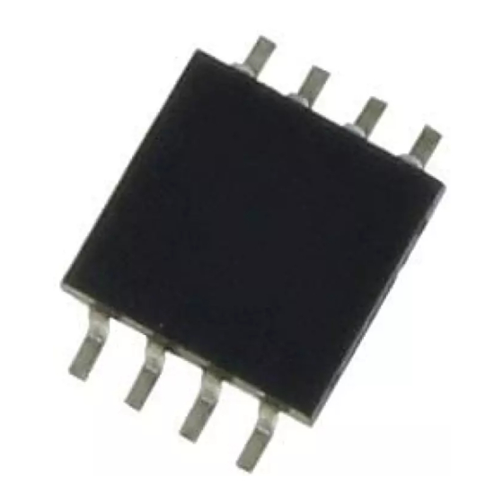
Summary of Contents for Toshiba TLP7820
- Page 1 RD014-RGUIDE-01 Isolation Amplifier Application Circuits (Voltage Sensing) of the TLP7820 Reference Guide RD014-RGUIDE-01 © 2018 2018-03-15 1 / 19 Toshiba Electronic Devices & Storage Corporation Rev. 1...
-
Page 2: Table Of Contents
Table of Contents 1. OVERVIEW ....................3 1.1 Target applications ......................3 2. MAJOR FEATURES OF THE TLP7820 .............. 4 3. APPLICATION CIRCUIT EXAMPLE AND ITS BILL OF MATERIALS....9 3.1 Example of an application circuit for voltage sensing ............9 3.2 Bill of materials ........................ -
Page 3: Overview
(MCU) more properly. The TLP7820 is an isolation amplifier which has optical coupled isolation feature in order to meet above requirement with 0.02% (typical) linearity accuracy. The TLP7820 also provides a common- mode transient immunity (CMTI) of 20 kV/μs (typical), therefore stable even in noisy motor control... -
Page 4: Major Features Of The Tlp7820
RD014-RGUIDE-01 Example of an application to an inverter Toshiba offers the TLP5214A photocoupler suitable for use as an IGBT gate driver. For details of the TLP5214A → Click Here 2. Major features of the TLP7820 Common-mode transient immunity (CMTI) ... - Page 5 ) with 4-kV/μs and 8-kV/μs slew rates are applied. As shown in Figure 2.2, V does not have much noise, which proves that the TLP7820 has enough CMTI performance to apply actual applications. dV/dt = 4 kV/μs dV/dt = 8kV/μs...
- Page 6 80 ns/div ) - (V ): 100 mV/div OUT+ OUT- Figure 2.3 Example of an output waveform of the TLP7820 when a common-mode voltage (V ) with a very large slew rate is applied About output linearity characteristics ...
- Page 7 Figure 2.5 Input voltage vs. output voltage deviation from the line of best fit is calculated as follows: From Figure 2.5, dev_max = 1.3 mV, dev_min = -1 mV, and V = 2.5 V, then: 0.0013 0.001 100 0.046% © 2018 2018-03-15 7 / 19 Toshiba Electronic Devices & Storage Corporation Rev. 1...
- Page 8 Figure 2. 6 shows the relationships between the input voltage and the primary-side supply current of the TLP7820 ( B) side) and a competitor’s isolation amplifier ( A) side). The primary-side supply current of the competitor’s isolation amplifier increases with input voltage...
-
Page 9: Application Circuit Example And Its Bill Of Materials
RD014-RGUIDE-01 of the TLP7820 remains around 9 mA regardless of input voltage change. For example, a floating power supply such as a bootstrap is used as a primary-side power supply for an isolation amplifier since the floating power supply allows the use of small-value capacitors to reduce the circuit size. -
Page 10: Bill Of Materials
TLP7820 to detect divided voltage with a divider. The voltage-sensing error is determined considering the tolerances of R1, R2, and R3 and the error of the equivalent input resistance R kΩ) across Pin 2 and GND of TLP7820. The followings are calculation examples of voltage-sensing resistors. -
Page 11: Test Mode Considerations
= 5V). Don't use the TLP7820 in such a condition. 5. Simulation 5.1 Basic operation This section shows the simulation results for verifying the basic operation of the TLP7820. Figure 5.1 shows the simulation circuit under the following conditions: ∎ Simulation conditions ·... - Page 12 Figure 5.2 shows the simulation results. The output is a 10kHz sine wave with 1.64Vp-p, which has x8.2 as large an amplitude as the input signal (10kHz sine wave) with 0.2Vp-p. This is equal to the specified typical gain of x8.2 of the TLP7820, indicating that simulation ran properly. 250mV 2.6V...
-
Page 13: Noise Superimposed On The Input Voltage
-50mV 1.4V -100mV 1.2V -150mV 1.0V -200mV 0.8V >> -250mV 0.6V 50us 100us 150us 200us 250us 300us V(Vin) V(Vout) Time Figure 5.4 Simulation waveforms with noise © 2018 2018-03-15 13 / 19 Toshiba Electronic Devices & Storage Corporation Rev. 1... -
Page 14: Circuit With Filters
The output is a 10kHz sine wave with 1.64Vp-p, which has x8.2 as large an amplitude as the input signal (10kHz sine wave) with 0.2Vp-p. This is equal to the specified typical gain of x8.2 of the TLP7820, indicating that simulation ran properly. © 2018... - Page 15 -150mV 1.0V -200mV 0.8V >> -250mV 0.6V 50us 100us 150us 200us 250us 300us V(Vin) V(Vout) Time Figure 5.6 Results of simulation of a circuit with filters © 2018 2018-03-15 15 / 19 Toshiba Electronic Devices & Storage Corporation Rev. 1...
-
Page 16: Product Overview
RD014-RGUIDE-01 6. Product overview 6.1. Overview The TLP7820 is an optically coupled isolation amplifier that has a high-precision delta-sigma AD converter at the primary side and a DA converter at the secondary side. Recommended supply voltage ranges: Primary side = 4.5 to 5.5 V, Secondary side = 3.0 to 5.5 V Operating temperature range: -40 to +105°C... -
Page 17: External View And Pin Assignment
Positive output OUT+ Output side supply voltage Figure 6.1 External view, marking, and pin assignment of the TLP7820 6.3. Internal block diagram Note: Add 0.1μF bypass capacitors between Pin 1 and Pin 4 and between Pin 5 and Pin 8. -
Page 18: Output Voltages For Different Primary- And Secondary-Side Power Supply Combinations
Primary-Side Power Primary-Side Power Supply, V Supply, V x Gain/2 x Gain/2 Secondary- Secondary- +2.5 V +1.25 (V) +1.25 (V) Side Power Side Power Supply Supply © 2018 2018-03-15 18 / 19 Toshiba Electronic Devices & Storage Corporation Rev. 1... - Page 19 RD014-RGUIDE-01 Terms of Use This terms of use is made between Toshiba Electronic Devices and Storage Corporation (“We”) and customers who use documents and data that are consulted to design electronics applications on which our semiconductor devices are mounted (“this Reference Design”). Customers shall comply with this terms of use. Please note that it is assumed that customers agree to any and all this terms of use if customers download this Reference Design.


Need help?
Do you have a question about the TLP7820 and is the answer not in the manual?
Questions and answers