Table of Contents
Advertisement
Quick Links
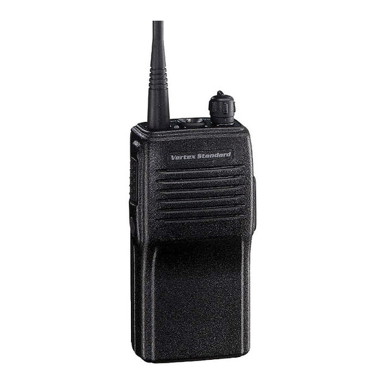
FM Business Two-Way Radio
VX-131/-132
VHF Model
Service Manual
©2004 VERTEX STANDARD CO., LTD.
Introduction
This manual provides technical information necessary for servicing the VX-131 and VX-132 VHF FM Transceiver.
Servicing this equipment requires expertise in handling surface-mount chip components. Attempts by non-qualified
persons to service this equipment may result in permanent damage not covered by the warranty, and may be illegal in
some countries.
Two PCB layout diagrams are provided for each double-sided circuit board in the transceiver. Each side of is referred to
by the type of the majority of components installed on that side ("leaded" or "chip-only"). In most cases one side has only
chip components, and the other has either a mixture of both chip and leaded components (trimmers, coils, electrolytic
capacitors, ICs, etc.), or leaded components only.
While we believe the technical information in this manual to be correct, VERTEX STANDARD assumes no liability for
damage that may occur as a result of typographical or other errors that may be present. Your cooperation in pointing out
any inconsistencies in the technical information would be appreciated.
Specifications ................................................... 2
Exploded View & Miscellaneous Parts ...... 3
Programming the Channel Data .................. 4
Cloning ............................................................. 6
Block Diagram ................................................. 7
EC059N90A
VX-131
VERTEX STANDARD CO., LTD.
4-8-8 Nakameguro, Meguro-Ku, Tokyo 153-8644, Japan
VERTEX STANDARD
US Headquarters
10900 Walker Street, Cypress, CA 90630, U.S.A.
YAESU EUROPE B.V.
P.O. Box 75525, 1118 ZN Schiphol, The Netherlands
YAESU UK LTD.
Unit 12, Sun Valley Business Park, Winnall Close
Winchester, Hampshire, SO23 0LB, U.K.
VERTEX STANDARD HK LTD.
Unit 5, 20/F., Seaview Centre, 139-141 Hoi Bun Road,
Kwun Tong, Kowloon, Hong Kong
VX-132
Circuit Description ................................. 9
Alignment ............................................... 13
Circuit Diagram ....................................................... 21
Parts Layout ............................................................. 23
Parts List ................................................................... 25
1
Advertisement
Table of Contents

Related Manuals for Vertex Standard VX-131


Summary of Contents for Vertex Standard VX-131
-
Page 1: Table Of Contents
ICs, etc.), or leaded components only. While we believe the technical information in this manual to be correct, VERTEX STANDARD assumes no liability for damage that may occur as a result of typographical or other errors that may be present. Your cooperation in pointing out any inconsistencies in the technical information would be appreciated. -
Page 2: Specifications
Specifications General Frequency Range: 150 - 174 MHz Number of Channels: 1 channel (VX-131), 2 channles (VX-132) Channel Spacing: 12.5 / 25 kHz Power Supply Voltage: 7.5 VDC ± 10% Operating Temperature Range: –22 °F to +140 °F (–30 °C to +60 °C) Frequency Stability: ±2.5 ppm... -
Page 3: Exploded View & Miscellaneous Parts
Exploded View & Miscellaneous Parts RA0631200 RA0631300 FRONT CASE ASSY (VX-132) FRONT CASE ASSY (VX-131) RA0173500 (w/PTT KNOB) (w/PTT KNOB) R6147510 RING NUT RA0294200 RA029430A RA0294200 PTT KNOB RUBBER PACKING PTT KNOB RA0110200 HOLDER RUBBER RA0296100 ΠVOLUME KNOB... -
Page 4: Programming The Channel Data
Programming the Channel Data The VX-131/-132 transceiver allows you to change the channel frequency and its CTCSS/DCS status. Also, you may select the channel bandwidth (wide/narrow) of all VHF frequencies and some UHF frequencies (see the channel table). If the channel programming process fails, the radio... - Page 5 You may check the CTCSS/DCS/ARTS status by press- ing and holding in the MONITOR button. The radio will respond with the CTCSS/DCS confirmation beeps according to the chart at the beginning of this section. VX-131 D VX-132 D EFALUT ETTING...
-
Page 6: Cloning
The VX-131/-132 series includes a convenient “Cloning” feature, which allows the programming data from one transceiv- er to be transferred to another VX-131/-132 series. Here is the procedure for cloning one radio’s data to another. 1. Turn both transceiver off. -
Page 7: Block Diagram
Block Diagram... - Page 8 Block Diagram...
-
Page 9: Circuit Description
Circuit Description Receive Signal Path Squelch Control Incoming RF signal from the antenna jack is delivered to The squelch circuitry consists of a noise amplifier and the MAIN Unit and passes through a low-pass filter con- band-pass filter within Q1040 (TA31136FN) and noise sisting of coils L1003 and L1006, capacitors C1009, C1012, detector D1026 (1SS355). - Page 10 Circuit Description The transmit signal then passes through the antenna switch PLL Frequency Synthesizer D1004 (RLS135) and is low-pass filtered to suppress har- The PLL circuitry on the Main Unit consists of VCO Q1003 monic spurious radiation before delivery to the antenna. (2SC5231), VCO buffer Q1006 (2SC5005), and PLL IC Q1005 (MB15A02PFV1) which contains a reference divid- CTCSS/DCS Signal Path...
- Page 11 Circuit Description Receive and transmit buses select which VCO is made active by Q1002 and Q1004 (both RT1N441U). TCXO unit X1001 yields frequency stability of ±2.5 ppm @ –30 °C to +60 °C. Push-To-Talk Transmit Activation The PTT switch S1002 is connected to pin 48 of micropro- cessor Q1013 (M37516F8HP), so that when the PTT switch is closed, pin 23 of Q1013 (M37516F8HP) goes low.
- Page 12 Circuit Description Note...
-
Page 13: Alignment
Alignment Introduction Required Test Equipment The VX-131/-132 has been aligned at the factory for the Radio Tester with calibrated output level at 500 MHz specified performance across the entire frequency range In-line Wattmeter with 5 % accuracy at 500 MHz specified. - Page 14 Alignment Set up the test equipment Menu of the Tool Set up the test equipment as shown below for transceiver RF Frequency alignment, and apply 7.5V DC power to the transceiver. Set the transceiver to “CH 2 (160.005 MHz)“ via the “...
- Page 15 Alignment Transmitter Output Power MAX Deviation Set the transceiver to “CH 2 (160.005 MHz)“ via the Set the transceiver to “CH 2 (160.005 MHz)“ via the “ ” box. “ ” box. Double click the left mouse button on the “ RF Power Inject a 1 kHz tone at –17 dBm to the MIC jack.
- Page 16 Alignment MIC Sensitivity CTCSS VCO Modulation Set the transceiver to “CH 2 (160.005 MHz)“ via the Set the transceiver to “CH 2 (160.005 MHz)“ via the “ ” box. “ ” box. Inject a 1 kHz tone at –37 dBm to the MIC jack. Activate the CTCSS encoder with “254.1 Hz“...
- Page 17 Alignment CTCSS Ref. Modulation DCS Deviation Set the transceiver to “CH 2 (160.005 MHz)“ via the Set the transceiver to “CH 2 (160.005 MHz)“ via the “ ” box. “ ” box. Activate the CTCSS encoder with “67.0 Hz“ Tone via Activate the DCS encoder with “627“...
- Page 18 Alignment RX Sensitivity Threshold NSQ Level (Wide) Set the transceiver to “CH 3 (173.995 MHz)“ via the Set the transceiver to “CH 2 (160.005 MHz/Wide)“ via “ ” box. the “ ” box. Injust a 160.005 MHz siganl at a level of 40dBµ with Injust a 160.005 MHz siganl at a level of –10dBµ...
- Page 19 Alignment Threshold NSQ Level (Narrow) Set the transceiver to “CH 5 (160.005 MHz/Narrow)“ via the “ ” box. Injust a 160.005 MHz siganl at a level of –10dBµ with ±1.5 kHz deviation with a 1 kHz to the Antenna Jack. Double click the left mouse button on the “...
- Page 20 Alignment Note...
-
Page 21: Main Unit
MAIN Unit Circuit Diagram 5.0 V 1.9 V 2.6 V 0.7 V 4.9 V 0.7 V 1.0 V TX (2 W): 1.7 V 3.9 V W: 3.1 V RX: 3.5 V W: 5.0 V RX: 0 V TX (2 W): 1.7 V N: 1.9 V TX: 0 V N: 1.2 V... - Page 22 MAIN Unit Note...
-
Page 23: Parts Layout
MAIN Unit Parts Layout (Side A) LM2902PWR NJM2070M 2SA1586Y (SY) CPH6102 (AB) IMZ2 (Z2) RT1N441U (N3) 12-22SURSYGC/S530-A2/TR8 (Q1017, 1030) (Q1041) (Q1012, 1037, (Q1039) (Q1029) (Q1036) (D1023) 1043) NJM12903R 2SC4154E (LE) FMW1 (W1) RD07MVS1 RT1P441U (P3) MC2850 (A7) (Q1045) (Q1022, 1035) (Q1031) (Q1024) (Q1034) - Page 24 MAIN Unit Parts Layout (Side B) M37516F8HP MB15A02PFV1 3SK320 (U7) 2SA1586Y (SY) 2SC4154E (LE) CPH6102 (AB) FMW1 (W1) RT1N441U (N3) S-80835CNMC DAN235E (M) (Q1013) (Q1005) (Q1026) (Q1010) (Q1007, 1008) (Q1020, 1027) (Q1021, 1028) (Q1004, 1023, (Q1032) (D1014) 1044) TA31136FN 2SC4215Y (QY) (Q1040) (Q1033) 2SC5005 (73)
-
Page 25: Parts List
MAIN Unit Parts List DESCRIPTION VALUE TOL. MFR'S DESIG VXSTD P/N VERS. LOT SIDE LAY ADR PCB with Components CB2910001 1 CH CB2910002 2 CH Printed Circuit Board AC059N000 FR0120800 C 1001 CHIP TA.CAP. 0.1uF TESVA1V104M1-8R K78160025 C 1005 CHIP CAP. 2.2uF ECJ2FB1A225K K22100807... - Page 26 MAIN Unit Parts List DESCRIPTION VALUE TOL. MFR'S DESIG VXSTD P/N VERS. LOT SIDE LAY ADR C 1080 CHIP CAP. 0.1uF GRM39B104K16PT K22124805 C 1081 CHIP CAP. 15pF GRM39CH150J50PT K22174215 C 1082 CHIP CAP. 0.0047uF GRM39B472K50PT K22174833 C 1083 CHIP CAP. 0.1uF GRM39B104K16PT K22124805...
- Page 27 MAIN Unit Parts List DESCRIPTION VALUE TOL. MFR'S DESIG VXSTD P/N VERS. LOT SIDE LAY ADR C 1172 CHIP CAP. 0.047uF GRM39B473K16PT K22124804 C 1173 CHIP CAP. 82pF GRM39CH820J50PT K22174233 C 1174 CHIP CAP. 0.0033uF GRM39B332K50PT K22174831 C 1175 CHIP CAP. 0.001uF GRM39B102K50PT K22174821...
- Page 28 Q 1026 3SK320(TE85L) G4803208 Q 1027 TRANSISTOR CPH6102-TL G3070223 Q 1028 TRANSISTOR FMW1 T98 G3070009 Q 1029 TRANSISTOR IMZ2A T108 G3070060 Q 1030 LM2902PWR G1094009 Q 1031 TRANSISTOR FMW1 T98 G3070009 Q 1032 S-80835CNMC-B8U-T2 G1093606 : Please contact Vertex Standard...
- Page 29 MAIN Unit Parts List DESCRIPTION VALUE TOL. MFR'S DESIG VXSTD P/N VERS. LOT SIDE LAY ADR Q 1033 TRANSISTOR 2SC4215Y TE85R G3342157Y Q 1034 TRANSISTOR RT1P441U-T11-1 G3070248 Q 1035 TRANSISTOR 2SC4154-T11-1E G3341548E Q 1036 TRANSISTOR RT1N441U-T11-1 G3070247 Q 1037 TRANSISTOR 2SA1586Y TE85R G3115867Y Q 1038...
- Page 30 MAIN Unit Parts List DESCRIPTION VALUE TOL. MFR'S DESIG VXSTD P/N VERS. LOT SIDE LAY ADR R 1070 CHIP RES. 1/16W RMC1/16 473JATP J24185473 R 1071 CHIP RES. 1/16W RMC1/16 273JATP J24185273 R 1072 CHIP RES. 220k 1/16W RMC1/16 224FTP J24183224 R 1073 CHIP RES.
- Page 31 MAIN Unit Parts List DESCRIPTION VALUE TOL. MFR'S DESIG VXSTD P/N VERS. LOT SIDE LAY ADR R 1150 CHIP RES. 3.3k 1/16W RMC1/16 332JATP J24185332 R 1151 CHIP RES. 1/10W RMC1/10T 680J J24205680 R 1152 CHIP RES. 1/16W RMC1/16 220JATP J24185220 R 1153 CHIP RES.
- Page 32 MAIN Unit Parts List DESCRIPTION VALUE TOL. MFR'S DESIG VXSTD P/N VERS. LOT SIDE LAY ADR R 1236 CHIP RES. 1/16W RMC1/16 000JATP J24185000 R 1265 CHIP RES. 1/16W RMC1/16 330JATP J24185330 R 1266 CHIP RES. 1/16W RMC1/16 000JATP J24185000 R 1267 CHIP RES.
- Page 34 Copyright 2004 VERTEX STANDARD CO., LTD. All rights reserved No portion of this manual may be reproduced without the permission of VERTEX STANDARD CO., LTD. Printed in Japan.
Need help?
Do you have a question about the VX-131 and is the answer not in the manual?
Questions and answers