Tektronix 2445 Instruction Manual
Service
Hide thumbs
Also See for 2445:
- Instruction manual (136 pages) ,
- Instruction manual (52 pages) ,
- Instruction manual (55 pages)
Table of Contents
Advertisement
Quick Links
Advertisement
Table of Contents
Troubleshooting

Subscribe to Our Youtube Channel
Related Manuals for Tektronix 2445


Summary of Contents for Tektronix 2445
- Page 1 Tektronix 2445 OSCILLOSCOPE SERVICE INSTRUCTION MANUAL...
- Page 2 OPERATORS SAFETY SUMMARY SERVICE SAFETY SUMMARY PRIOR PERFORMING ANY SERVICE. PLEASE CHECK FOR CHANGE INFORMATION AT THE REAR OF THIS MANUAL. 2445 OSCILLOSCOPE SERVICE INSTRUCTION MANUAL Tektronix, Inc. P.O. Box 500 Beaverton, Oregon 97077 Serial Num ber_____________________ 070-3829-00 Product Group 38...
- Page 3 Copyright © 1983 Tektronix, Inc. All rights reserved. Contents of this publication may not be reproduced in any form without the written permission of Tektronix, Inc. Products of Tektronix, Inc. and its subsidiaries are covered by U.S. and foreign patents and/or pending patents. TEKTRONIX, TEK, SCOPE-MOBILE, and registered trademarks of Tektronix, Inc.
-
Page 4: Table Of Contents
2445 Service TABLE OF CONTENTS Page Page LiST OF IL L U S T R A T IO N S ........... iv OPERATOR'S CHECKS AND ADJUSTM ENTS.......2-17 LIST OF TAB LES.............. v IN TR O D UC TIO N ......... 2-17 OPERATORS SAFETY S U M M A R Y ......vi... - Page 5 2445 Service TABLE OF CONTENTS (cont) Page Page DYNAMIC CENTERING, SECTION 3 T H E O R Y OF O PERATIO N (cont) CRT TERMINATION, LOW VOLTAGE VER TICAL GAIN, R E G U LA T O R S ........3-45 VERTICAL CENTERING, POWER D IS TR IB U TIO N .....3-47...
- Page 6 2445 Service TABLE OF CONTENTS (cont) Page SECTION 7 OPTIONS SECTION 8 REPLACEABLE ELECTRICAL PARTS , „ SECTION 9 DIAGRAMS INTRODUCTION..OPTION 2 2 ....SECTION 10 REPLACEABLE MECHANICAL PARTS OPTION 1 R ....ACCESSORIES POWER CORD OPTIONS FUTURE OPTIONS..
-
Page 7: List Of Illustrations
LIST OF ILLUSTRATIONS Figure Pa9e The 2445 Oscilloscope........................v'*i Line selector switch, line fuse, and detachable power cord............2-2 Power and display c o n tro ls ......................2-4 Vertical controls and CH 1 OR X and CH 2 connectors..............2-5 Channel 3 and Channel 4 controls and connectors and CALIBRATOR o u t p u t ....... - Page 8 2445 Service LIST OF TABLES Table Page Electrical Characteristics........................1-2 Environmental Characteristics......................i-1u Mechanical Characteristics........................ 1-11 2- 1 Voltage, Fuse, and Power-Cord Data....................2-3 3- 1 Intensity Control..........................3-20 Trigger Source Selection........................3-21 Vertical Display Selection........................3-24 Horizontal Display Selection......................3-25 Blanking and Intensity Control Selection..................3-26 Readout Display Mode S election......................
-
Page 9: Operators Safety Summary
2445 Service OPERATORS SAFETY SUMMARY The general safety information in this part o f the summary is fo r both operating and servicing personnel. Specific warnings and cautions w ill be found throughout the manual where they apply and do n ot appear in this summary. -
Page 10: Servicing Safety Summary
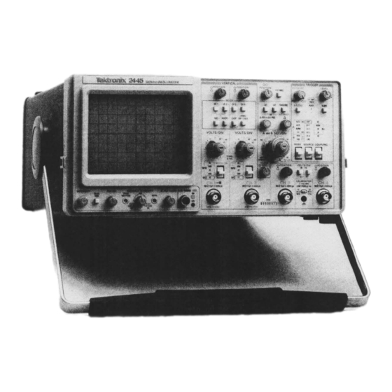
2445 Service SERVICING SAFETY SUMMARY FOR QUALIFIED SERVICE PERSONNEL ONLY Refer also to the preceding Operators Safety Summary. Disconnect power before removing protective panels, Do Not Service Alone soldering, or replacing components. Do not perform internal service or adjustment of this product unless another person capable of rendering first aid and resuscitation is present. - Page 11 2445 Service 3829-01 The 2445 Oscilloscope,...
-
Page 12: Section 1 Specification
(Table 1-1) are valid for the 2445 when it has been adjusted at an The horizontal deflection system provides calibrated ambient temperature between +20°C and +30°C, has had sweep speeds from 1.5 s per division to 1 ns per division. - Page 13 Specification—2445 Service Table 1-1 Electrical Characteristics Characteristics Performance Requirements V E R T IC A L D EFLEC TIO N S Y S T E M -C H A N N E L 1 A N D C HA NN EL 2...
- Page 14 Specification— 2445 Service Table 1-1 (cont) Characteristics Performance Requirements VERTICAL DEFLECTION SYSTEM -CHANNEL 1 AND CHANNEL 2 (cont) Common-mode Rejection Ratio (CMRR) A t least 20:1 at 50 MHz for common-mode signals of eight divisions or less, w ith VAR VO LTS/DIV control adjusted fo r best CMRR at 50 kHz at any VO LTS/DIV switch setting from 5 mV to 5 V;...
- Page 15 Specification—2445 Service Table 1-1 (cont) Performance Requirements Characteristics VERTICAL DEFLECTION SYSTEM -CHANNEL 3 AND CHANNEL 4 (cont) Step Response 2.33 ns or less (calculated from bandwidth).3 Rise Time 50:1 or greater attenuation of the deselected channel at 100 MHz Channel Isolation w ith an eight-division input signal.
- Page 16 Specification— 2445 Service Table 1-1 (cont) Characteristics Performance Requirements TRIGGERING (cont) Minimum P-P Signal Amplitude fo r Stable Triggering Amplitudes are one-half o f Channel 1 or Channel 2 source from Channel 3 or Channel 4 Source specification. Minimum P-P Signal Am plitude fo r Stable Triggering Add 1 division to single-channel source specifications.
- Page 17 Specification—2445 Service T -L I- 1 I d u ic I s I \i# C n i/ Performance Requirements Characteristics TRIGGERING (cont) AUTO Mode Maximum Triggering Signal Period A SEC/DIV Switch Setting Less than 10 ms A t least 80 ms.a A SEC/DIV Switch Setting from 10 ms to 50 ms A t least 16 times the A SEC/DIV switch setting.3...
- Page 18 Specification— 2445 Service Table 1-1 (cont) Performance Requirements Characteristics HORIZONTAL DEFLECTION SYSTEM (cont) Add ±2% of time interval to all accuracy specifications. Timing Accuracy (A SEC/DIV switch set to 1 s per division) Add 2% o f time interval to the A and B Sweep Accuracy Timing Accuracy (SEC/DIV VAR control out of specification.
- Page 19 Specification—2445 Service Table 1-1 (cont) Performance Requirements Characteristics Z-AXIS INPUT Sensitivity Dc to 2 MHz Positive voltage decreases intensity; +2 V blanks a maximum- intensity trace. +2 V modulates a normal-intensity trace.3 2 MHz to 20 MHz Input Resistance 9 k£2 ±10%.a ±25 V peak;...
- Page 20 Specification— 2445 Service Table 1-1 (cont) Characteristics Performance Requirements Display 80 mm x 100 mm.a Standard Phosphor P31.a Nominal Accelerating Potential 16 kV.a AC POWER SOURCE Source Voltage Ranges 115 V 90 V to 132 V.a 230 V 180 V to 250 V.a...
- Page 21 Environmental Characteristics Characteristics Performance Requirements The 2445 Oscilloscope meets the environmental requirements of MIL-T-28800C for Type III, Class 3, Style C equipment; tested as per paragraph 4.5.5.1.2.2 fo r hum idity, 4.4.5.1.3 for low temperature, and 4.5.5.1.4 fo r high temperature.
- Page 22 With Front-Panel Cover 434 mm (17.1 in). With Handle Extended 505 mm (19.9 in). Cooling Forced-air circulation. Finish Tektronix Blue vinyl-clad material on aluminum cabinet. Construction Aluminum alloy chassis (sheet metal). Plastic laminate fron t panel. Glass laminate circuit boards. 1-11...
-
Page 23: Preparation For Use
This section of the manual provides information on instrument installation and power requirements; and the functions of controls, connectors, and indicators are described. Operating considerations, intended to familiarize the operator w ith basic measurement techniques, and operator's checks and adjustments fo r the 2445 are included. For additional operating information, refer to the 2445 Operators Manual. -
Page 24: Instrument Cooling
Appendix A o f the Operators Manual. Consult your service fan-exhaust holes in the rear panel are free of any obstruc department, your local Tektronix Service Center, or nearest tion to airflow. Tektronix representative if additional assistance is needed. -
Page 25: Voltage, Fuse, And Power-Cord Data
Operating Inform ation-2445 Service 2. If the instrument is to be shipped to a Tektronix 4. Cushion the instrument on all sides by tightly packing Service Center for service or repair, attach a tag to dunnage or urethane foam between the carton and the instrument showing the following: owner of the the instrument, allowing three inches on each side. -
Page 26: Controls, Connectors, And Indicators
Operating Information—2445 Service CONTROLS, CONNECTORS, AND INDICATORS The following descriptions are intended to familiarize ( T ) SCALE ILLU M C ontrol-Adjusts the light level of the operator w ith the location and function of the instru the graticule illumination. -
Page 27: E R T Ic A L
Deflection factors shown in the crt readout reflect connected. internal circuitry recognizes actual deflection factors in use when Tektronix Tektronix attenuation-coded probes. attenuation-coded probes are connected to the inputs. Input Coupling Switches and Indicators— Select the (?3) VAR Controls—Provide continuously variable, un... -
Page 28: Channel 3 And Channel 4 Controls And Connectors And Calibrator O U T P U T
Operating Inform ation— 2445 Service The position of this switch has no effect on the MODE Switches—Select the indicated channel (s) switching rate o f m ultiple X-Y displays. When more fo r display when latched in. Any combination of the... -
Page 29: Horizontal And Delta Measurement
POS control. jitte r and w ill give false (low) frequency counts The sweep o f the 2445 is easily shut o ff by set ting the TRIGGER MODE switch to SGL SEQ. For single-trace displays, when either the Delta... - Page 30 Operating Inform ation— 2445 Service j-f gj+hor /\+ qr i/^ + j$ jso activated intensified gppoar the A Sweep if the B TRIGGER MODE is set to RUN AFT DLY. When the B TRIGGER zones and associated B Sweeps w ill be established MODE is set to TRIG AFT DLY, intensified zones in the same manner as described in "PULL-...
- Page 31 Operating Inform ation— 2445 Service (2?) X10 MAG Switch—Horizontally magnifies the por tw o separate delay times are established by the tion of the sweep display positioned at the center Delta Time function. One cursor position (or delay vertical graticule line by a factor of 10 when pressed time) is set by the A REF OR D LY POS control, in.
-
Page 32: Trigger
Operating Information—2445 Service \o2j peak-reference levels and the trigger level are A Control— Sets the alternate B Sweep delay time or redefined whenever triggering ceases, whenever the positions the Delta-time cursor (vertical line) when LEVEL control is turned to either extreme, or either the A t or 1/A t Measurement Mode is active. - Page 33 Operating Inform ation— 2445 Service set to GND or when the input coupling o f both When A L T VER TICAL MODE is selected, each Channel 1 and Channel 2 is set to GND, w ith displayed channel in turn provides the triggering...
-
Page 34: Rear Panel
Operating Information—2445 Service circuitry; it aiiows stabie triggering on the iow- ^38^ LEVEL Control— Sets the amplitude point on the triggering signal at which either A or B Sweep trig frequency components of a complex waveform. gering occurs. This control produces fine resolution for a portion of its range, after which it changes to LF REJ—... -
Page 35: Readout Display
Operating Inform ation— 2445 Service ?) CH 2 SIGNAL OUT Connector—Provides an output (46) Fuse Holder—Contains the ac power-source fuse. signal that is a normalized representation o f the Channel 2 input signal. The output amplitude into a 1-M£2 load is approximately 20 mV per division ) Detachable Power Cord Receptacle—Provides the... -
Page 36: Readout Display Locations
Operating Information—2445 Service The locations and types o f information displayed under The Trigger-Level readout shows the signal voltage normal operating modes are illustrated in Figure 2-8. (at the probe tip o f encoded probes) that w ill initiate the sweep. The readout appears only if the following con... -
Page 37: Operating Considerations
GROUNDING The most reliable signal measurements are made when the 2445 and the unit under test are connected by a com mon reference (ground lead) in addition to the signal lead or probe. The probe's ground lead provides the best... -
Page 38: Input-Coupling Capacitor Precharging
Operating Information—2445 Service PI/MUAI AAlUMrr'TIAMC O I U I V M L I IV M V O quality, low-loss coaxial cables should be used. Coaxial cables should be terminated at both ends in their char Probes acteristic impedance. If this is not possible, use suitable Generally, probes offer the most convenient means of impedance-matching devices. -
Page 39: Operator's Checks And Adjustments
Operating Inform ation— 2445 Service OPERATOR'S CHECKS AND ADJUSTMENTS INTRODUCTION Horizontal A AND B SEC/DIV Locked together at 1 ms SEC/DIV VAR Calibrated detent This part contains procedures that may be used to verify POSITION Midrange the operation and basic accuracy of your instrument before... -
Page 40: Auto Dc Balance Adjustment
"In itia l Setup." Set 20 MHz BW LIM IT On (in). AUTO DC BALANCE ADJUSTMENT The 2445 can automatically perform a dc-balance Connect the two 10X probes (supplied with the adjustment of Channel 1 and Channel 2. This adjustment instrument) to the CH 1 OR X and the CH 2 input con... -
Page 41: Matching Channel 2 Delay
CORRECT \ U NDER C O M P E N S ATE 3 / NOTE The 2445 can be set to preclude operator adjustment o f Channel 2 delay. I f the delay-offset feature is 1 0 0 rn V... -
Page 42: Amplitude Check
Set X I 0 fviAG ON (button in) and adjust the A control until the tw o signals are overlaid horizontally. The CALIBRATOR signal on the 2445 automatically changes repetition rate w ith the setting of the A SEC/DIV NOTE switch w ithin the range of 100 ms to 100 ns. -
Page 43: Introduction
TRUE (or 1) state; the more negative level is the FALSE required by the 2445. The High Voltage Power Supply (or 0) state. In the logic descriptions, the TRUE state is circuit develops the high accelerating potentials required referred to as HI, and the FALSE state is referred to as LO. -
Page 44: Block Diagram
Theory of Operation—2445 Service 3831-10A Figure 3-1. Block diagram. - Page 45 Theory of Operation—2445 Service 3831-10B Figure 3-1. Block diagram (cont).
- Page 46 Theory of Operation—2445 Service Most of the activities of the 2445 are directed by a (a specialized integrated circuit) which responds by setting up the various signals that control the stages handling the Microprocessor, Microprocessor, under firmware control (firmware is the programmed instructions contained real-time display signals.
-
Page 47: Detailed Circuit Description
2445 Oscilloscope. Circuitry unique to the 2445 is described in detail, while circuits common in the electronics industry are not. The descriptions are accom The clock signal is developed by the Microprocessor panied by supporting illustrations and tables. - Page 48 Theory o f Operation— 2445 Service hi iffororl As th e ooeratinn wnltanpc are fallin n th e Reset c irc u itrv ' *V Wf'TVI M VII ' " " O f • • • ' * * and inverted by U2556B to provide the 10-MHz clock must not generate a false RESET signal to the processor.
-
Page 49: Addres Decoding.
Theory of Operation—2445 Service is suspected of causing a system failure) or fo r trouble various devices and circuit functions. The controlling signals shooting the Address Bus and Address Decode circuitry. are generated as a result of the Microprocessor placing Removing the jumper removes the operating power from specific addresses on the Address Bus. - Page 50 Theory of Operation—2445 Service selected ROM is enabled, and data from the selected Address Decode description.) Instructions are read out of address location is read out of the ROM. the enabled ROM (or PROM) 1C from the address location present on its 13 address input pins (AO through A12).
-
Page 51: Analog Control
Theory of Operation— 2445 Service data from the Microprocessor is applied asynchronously If all the tasks are not completed at the end of one inter rupt cycle, the real-time interrupt request restarts the to the buffered Data Bus. A t the end of the write cycle, the analog updates, but as soon as those are accomplished, R/W signal goes HI, and the reset to U2468B is removed. - Page 52 The SI (scope identification) b it is checked at power-up performs a binary search routine that changes the output to determine if the instrument is a 2445. Some parts o f the voltage from the DAC in an orderly fashion until it most firmware are shared w ith a similar instrument, the 2465, closely approximates the voltage from the pot.
-
Page 53: Accept Address Tim In G
U2008 provides nonvolatile storage for the calibration least-significant digit (see Figure 3-3). constants and the power-down front-panel settings. When power is applied to the 2445, the Microprocessor reads the calibration constants and generates control voltages to set up the analog circuitry. The front-panel settings that were... -
Page 54: Front-Panel Controls
Theory o f Operation— 2445 Service Internal address decoding within U2008 then enables the the calibration routines) programmed into the read-only selected address location. The three mode-control bits are memory (ROM). These routines are explained in the Maintenance section of this manual. -
Page 55: Front-Panel Switch M A Tr Ix
Theory of Operation—2445 Service Like the switch matrix scanning, the Front-Panel pot When producing the actual analog control levels, the scanning routine is performed every 32 ms. When entered, processor can manipulate the digital values read fo r the the routine reads the settings of the last-moved pot and one various pots before sending the output data to the DAC. -
Page 56: Attenuators And Preamplifiers
Theory of Operation— 2445 Service iast pot moved, a fine-resoiution control voltage results. pattern to be displayed to the user. A LQ at any Q output In the fine-resolution range, a given rotational displacement of the registers illuminates the corresponding front-panel w ill cause a small control voltage change. - Page 57 U150: one to produce the functions of the 2445. Included in these functions are: CTC signal and the other to control the scale illumination attenuation factors, Channel 3 and Channel 4 gains, vertical- circuit during SGL SEQ display mode.
- Page 58 Theory of Operation—2445 Service Channel 2 Preamplifier Two analog control voltages set by the DAC and the Channel 1 vertical position dc level modify the differential Operation of Channel 2 Preamplifier U200 is nearly output signal at pins 9 and 10. The front-panel Channel 1...
-
Page 59: Display Sequencer, Triggers, And Sweeps
Theory of Operation— 2445 Service Scale Illumination collectors of U130D and U130E. As the SCALE ILLUM pot is advanced, the base drive to U130D and U130E The Scale Illumination circuit consists o f U130C, increases, and the voltage on their collectors moves closer U130D, U130E, U130F, and associated components. - Page 60 Theory of Operation—2445 Service Display Sequencer U65Q controls the various functions Readout Control defined by the data fields by setting the levels of the The vertical selection, horizontal selection, and intensity associated control lines. The functions and controlling controls are all set to their readout modes either at the...
- Page 61 Theory of Operation— 2445 Service used to set the charging current fo r holdoff-ramp inte to generate the delay gates that control each sweep's grating capacitor C660. A control voltage from digital-to- functions. analog converter (DAC) U2234 (diagram 2) via multiplexer U170 (diagram 4) is stored on C l 80.
-
Page 62: Intensity Control
Theory of Operation—2445 Service BLANK output signal (pin 3) is controlled by the readout Table 3-1 blank (ROB) signal from the Readout circuitry, and the Intensity Control readout intensity (ROI) signal (pin 23) controls the Type Resulting Current Horizontal BRIGHT output level. -
Page 63: Trigger Source Selection
The skew can be elimi Sweep is completed, the A Sweep Gate (SGA) from A nated by setting the 2445 to SGL SEQ Mode (to shut o ff Sweep hybrid U700 (via U980A) w ill go HI, causing the the sweeps). - Page 64 Theory of Operation— 2445 Service field stored in the internal control register of U700. The Q709, Q741. U860A.. U910B, U980A, and associated components. derived output current (M x ITREF) is connected to another programmable current-mirror circuit, U910B, external to the hybrid. The output of U910B provides...
-
Page 65: Vertical Channel Switch And Output Amplifiers
CALIBRATOR signal on the instrument providing the signal (since the skew occurs during sweep-retrace time), but it should be taken into account when using the 2445 B Sweep CALIBRATOR signal w ith other instrumentation. The skew can be eliminated from the signal by setting the 2445 Operation of B Sweep hybrid U900 is similar to that just TRIGGER MODE to SGL SEQ (to shut o ff the sweeps). -
Page 66: Vertical Display Selection
Theory of Operation—2445 Service T3hj8 3.3 Thp n iitn n t cinnal /pithor thp rpprlmit wartiral cinnal ,,,w 3* ■ « . v. w. the ground reference level) is applied to the CH5+ input of Vertical Display Selection Channel Switch U400 via R495 and R412. The inverting... -
Page 67: Sweep Generator
Table 3-4 Horizontal Display Selection BEAM FIND. As an aid in locating off-screen or over scanned displays, the 2445 is provided w ith a beam-finding Control Level feature. When the front-panel BEAM FIND button is Selected pushed, the beam-find input pin (BF, pin 15) o f U600 w iii Signal be pulled HI. -
Page 68: Blanking And Intensity Control Selection
Theory o f Operation— 2445 Service Switching between unmagnified (X I) gain and magnified its display sequence. The BRIGHT (brightness) signal ( X I0 gain) is also controlled by signals from the Display applied to U950 pin 44 from the Display Sequencer U650 (diagram 5) is amplified to the level required to drive the Sequencer. -
Page 69: Readout
Theory of Operation—2445 Service code written to each location in RAM points to a block of Focus tracking fo r intensity (VZOUT) level changes is provided by the VQOUT (quadrapole output voltage) signal addresses in Character ROM U2930. This block in the ROM contains the dot-position information fo r the specific at pin 22 of U950. -
Page 70: Developing The Readout D Is P La Y
Theory of Operation-2445 Service character address register U2960 (though they have not Character RAM. With U2865 loaded with the mode data, a been shifted into their correct positions fo r addressing final ROS1 strobe clocks the eighth b it of character data the RAM). - Page 71 Theory of Operation— 2445 Service The character data register U2860 also provides a means been displayed. As the last dot of a character is addressed, for the Microprocessor to read data from the Character the EOCH bit at pin 2 of U2855A goes LO. The next...
- Page 72 Theory of Operation—2445 Service The counter increments through the block of dot- The eight bits o f position data are w ritten to the perma nently enabled DAC each time a new dot is requested by position data until the last byte of the block is encountered the Dot Cycle Generator.
-
Page 73: Readout Display Mode S Election
Theory o f Operation— 2445 Service B HI. The HI outputs of U2900B and C applied to the Horizontal-positioning voltages fo r one segment of the select input pins of analog switch U2805 cause the Hori cursor are routed from Horizontal DAC through analog... -
Page 74: Readout Display Priorities
Theory of Operation—2445 Service idea!!'/, readout information should be displayed only Ac the Dot Cycle Generator runs, it resets U2830B in when the oscilloscope is not trying to display waveform the Dot Timer at somewhat irregular intervals w ith the traces. -
Page 75: Timing Of Refresh P Rioritizer
Theory of Operation— 2445 Service * N 0 T E : I F S0 IS ALSO HI AT T H IS TIME > THE PRIO RITY DOES NOT CHANGE. 5831-06 Figure 3-9. Timing of Refresh Prioritizer. If a second ROSFRAME request occurs before the... - Page 76 Theory o f Operation— 2445 Service signal that a new dot display is allowed. The HI from A similar readout display request w ill be generated when U2970C enables most of the gating in the Dot Start priority-two-or-higher displays are required when sweep Governor.
-
Page 77: High Voltage Power Supply And Crt
Theory of Operation— 2445 Service The two least-significant bits of the Dot Timer, from A t 1.4 jus after STARTDOT goes HI, U2995 pin 13 U2830B pins 11 and 10, are reset at the beginning of a (QH) goes HI to produce the REST signal, indicating that dot cycle by a LO STARTDOT signal applied to the reset the current dot cycle is complete and the Dot Cycle Gener... - Page 78 Theory of Operation— 2445 Service OSCILLATION START-UP. Initially, when power is If the Cathode Supply voltage level tends too positive, applied, the High Voltage Regulator circuit detects that the a slightly positive voltage w ill develop across C1932. This crt cathode voltage is too positive and pulls pin 6 of trans...
- Page 79 Theory o f Operation— 2445 Service to +4.66 kV. Following cycles continue to boost up DC Restorer succeeding capacitors to values 2.33 kV higher than the The DC Restorer provides crt control-grid bias and preceding capacitor until all six capacitors are fu lly charged.
-
Page 80: Dc Restorer Circuit.
Theory of Operation— 2445 Service on C l990 dissipates slowly; therefore, if instrument power Operational amplifier U189QA sinks a time-dependent is turned o ff and then immediately back on again, the variable current away from the base node of Q1980 that... - Page 81 Theory of Operation— 2445 Service decreased voltage across capacitor D decreases the potential The ac waveform, now carrying both the grid-bias information and the Z-Axis drive information, is applied difference between the control grid and the cathode, and to a DC Restorer circuit in the High Voltage Module where more crt beam current is allowed to flow.
-
Page 82: Low Voltage Power Supply
The Preregulator Control circuit consists primarily of control 1C U1030, its switching buffers, and its power The low voltages required by the 2445 are produced supply components. The control 1C senses voltage on the by a high-efficiency, switching power supply. This type of primary winding of T2060 and varies the "on tim e"... -
Page 83: Timing Relationships Of The Inverter Drive Signals
Theory o f Operation— 2445 Service The +21-V level begins to drain down as the control CR1022. The turns ratio of T1050 sets the secondary voltage at approximately +15 V; and, as long as the supply 1C draws current from C1025. If the Preregulator Control... -
Page 84: Simplified Schematic O F Control N E Tw O Rk
Theory of Operation— 2445 Service As the Prereguiator power supply turns on, capacitor During the startup, capacitor Cl 072 acts as a substantia! C l034 charges from the +5-V reference level toward load, and a relatively large current w ill flow in the windings ground potential through R1034 and R1037. - Page 85 Theory of Operation— 2445 Service negative-going pulse that turns o ff switching transistor primary winding w ill follow. Should the FB signal level Q1050 fo r a portion of each switching cycle. This o ff time tend too high, opposite control responses occur. Further...
- Page 86 Theory of Operation— 2445 Service Out-of-phase input signals to comparator U1062Ccome CR1132 is referenced at approximately +45 V through from two resistive voltage dividers placed in either leg of diode CR1131 (to the +42-V unregulated supply). As the one secondary winding of T1050. The comparator detects...
-
Page 87: Low Voltage Regulators
Theory of Operation— 2445 Service LOW VOLTAGE REGULATORS Q1222 w ill be biased into the active region. As Q1222 turns on, base drive for the Darlington pair (Q1221 and pass transistor Q1220) is reduced. The output w ill be held at... - Page 88 Theory of Operation—2445 Service +42-V supply is maintained, preventing component damage —8 V Regulator in the load circuitry. Should the +42-V supply be pulled Operation of the — 8 V Regulator is similar to that of the below +15 V (excessive loading or supply failure), the +-87 V and +42 V Regulators.
-
Page 89: Power Distribution
Schematic diagrams 11 and 12 illustrate the power and drives the output of U1371D high. The output level distribution of the 2445. The connections to the labeled from U1371D turns on Q1376 and pulls the PWR UP signal boxes (representing the hybrids and ICs) show the power to the Microprocessor LO. -
Page 90: Introduction
Section 4—2445 Service PERFORMANCE CHECK AND FUNCTIONAL VERIFICATION PROCEDURE INTRODUCTION This procedure is used to verify proper operation of instrument controls and to check the instrument’s performance against the requirements listed in the “Specification” (Section 1). This procedure verifies instrument function and may be used to determine need for readjustment. -
Page 91: Test Equipment Required
Performance Check— 2445 Service Table 4-1 Test Equipment Required item and Minimum Specification Example of Applica Description ble Test Equipment TEKTRONIX PS 503A. 1. Variable Power Variable output voltage: 0V to + 16V. Check input overload Supply switching. 2. Leveled Sine-Wave Frequency: 50 kHz to 150 MHz. - Page 92 Performance Check— 2445 Service Table 4*1 Test Equipment Required Item and Minimum Specification Example of Applica Description ble Test Equipment 19. Low-Capacitance Shaft length: 2 in. Adjust variable resistors TEKTRONIX Part Alignment Tool Number 003-0675-00. and capacitors. 20. IX Probe Attenuation: IX.
-
Page 93: V E R T I C A L
Mini Probe Tip-to-BNC Adapter (Item 12) Calibration Generator (Item 3) BNC Female-to-BNC Female Adapter (Item 13) P6131 10X Probe (supplied with 2445) (Item 6) BNC Female-to-Dual Banana Adapter (Item 14) Precision 50 ft BNC Cable (Item 8) 2X Attenuator (Item 15) - Page 94 Performance Check— 2445 Service N OTE Prior to performing the following steps, the 10X probe must be properly compensated. Refer to “Probe Low- To prevent damage to the input circuitry when in 50 Q Frequency Compensation in Section 2 o f this DC, the 20 V source must not be applied to the CH 1 manual.
- Page 95 Performance Check—2445 Service Use the VERTICAL POSITION control to set the VERTICAL MODE On (button in) bottom of the signal 2 divisions below graticule BW LIMIT center. On (press and release for a AV readout) Rotate the AREF OR DLY POS control to align the VOLTS/DIV reference cursor with the bottom of the waveform.
- Page 96 Performance Check— 2445 Service 23. Press and release the AV pushbutton to reobtain the CHECK— Display amplitude reduces to 2 divisions or AV readout display. less when the VOLTS/DIV VAR control (of the channel un der test) is rotated fully CCW. Return the VOLTS/DIV VAR 24.
-
Page 97: Ch 3 And Ch 4 Accuracy Limits
Performance Check— 2445 Service m, CHECK— Signal display amplitude is 1.9 to 2.1 ■ divisions. VOLTS/DIV CH 1 and CH 2 n. Move the test signal to CH 2 and set the VERTICAL VERTICAL MODE MODE controls to display CH 2. - Page 98 Performance Check— 2445 Service gg. Set the VERTICAL POSITION control to align the Pull the B SEC/DIV knob out to activate the CH 2 bottom edge of the signal display with the bottom graticule DLY feature. line. NO TE hh. CHECK— Signal display amplitude is 1.9 to 2.1 If the readout displays “CH 2 DLY D ISA B LED "...
- Page 99 Performance Check— 2445 Service d. CHECK— Signal display amplitude is 4.25 divisions or r. Adjust probe compensation for the best flat top on the greater. square-wave signal display. e. Move the signal to the CH 2 input connector and set s.
- Page 100 Performance Check— 2445 Service d. CHECK—Amplitude of each trace other than CH 1 is Set the generator output level for an 8-division display 0.08 division or less (discount trace width). of the reference signal on CH 1. Move the signal to the CH 2 input connector and Adjust either the CH 1 VAR control or the CH 2 VAR change the TRIGGER SOURCE switch to CH 2.
- Page 101 Performance Check—2445 Service VOLTS/DIV 8. Set CH 1 and CH 2 DC Balance. CH 1 and CH 2 2 mV NO TE Input Coupling CH 1 50 G DC For an accurate DC Balance setting, the instrument CH 2 1 Mfl DC M U S T be allowed to warmup for 2 0 minutes before performing the following steps.
- Page 102 Performance Check—2445 Service A and B SEC/DIV (knobs locked) n. Connect a 50 kHz signal from the Leveled Sine-Wave Generator to the CH 2 input connector via a precision 50 VOLTS/DIV BNC cable and a 10X attenuator. CH 2 10 mV o.
-
Page 103: Triggering
+ (plus) For each combination listed in the table, set the gener MODE AUTO LVL ator Test Frequency and the 2445 TRIGGER COUPLING as SOURCE VERT indicated, performing the following steps to verify the Trig gering levels in each setup. -
Page 104: Ch 1 Or Ch 2 Triggering C Onditions
Performance Check— 2445 Service Set the VOLTS/DIV switch and the generator output h. Repeat the DC TRIGGER COUPLING tests of Table level to obtain the test signal amplitude indicated for the 4-4 while in the ADD mode. particular combination being tested. - Page 105 Performance Check— 2445 Service r>:_. i« u .. . o. Puii the B SEC/DiV knob out and set it 1 switch set u. Connect the Leveled on ie - w a v e u e n e i m u i...
- Page 106 Performance Check— 2445 Service b. Connect the Function Generator to the CH 1 input via TRIGGER a 50 Q BNC cable, a 50 S 2 termination, and a 10X attenuator. MODE AUTO LINE SOURCE COUPLING c. Set the Function Generator output frequency and VOLTS/DIV level for a 50-kHz, 4-division display.
-
Page 107: Horizontal
Performance Check— 2445 Service HORIZONTAL Equipment Required (see Table 4-1) Leveled Sine-Wave Generator (Item 2) Time-Mark Generator (Item 5) Calibration Generator (Item 3) Precision 50 fi BNC Cable (Item 8) Initial Control Settings. b. Adjust the TRIGGER LEVEL control as necessary for a stable signal display. - Page 108 Performance Check— 2445 Service b. Select 5 ns time markers from the Time-Mark Genera NO TE tor and adjust the TRIGGER LEVEL control for a stable If the 2nd and 10th time markers are within ± 0 .0 6 display.
-
Page 109: Settings For A And B Timing Accuracy Checks And A Cursor Accuracy L Im Its
Performance Check— 2445 Service Table 4-6 Settings for A and B Timing Accuracy Checks and A Cursor Accuracy Limits A and B SEC/ Unmagnified DIV Switch Limits of At Cursor Time Limits of At Cursor Time Readout Markers Readout Markers... -
Page 110: Horizontal Timing Accuracy Checked Against The G Ra Tic U Le
Performance Check— 2445 Service Table 4-7 Horizontal Timing Accuracy Checked Against the Graticule Over Any 1 Div 2 Div 3 Div 4 Div 5 Div 6 Div 7 Div 8 Div 9 Div 10 Div Time-marker Accuracy ± 0.07 ± 0.07 ±... -
Page 111: Delta Time Display Accuracy
Performance C h e c k -2 4 4 5 Service On (button in) X10 MAG Delta Time Display Accuracy Off (DLY readout) TRIGGER Time- AUTO LVL MODE Marker Marker VERT SOURCE Period Super- COUPLING and A B SEC/ imposed SLOPE + (plus) SEC/DIV... -
Page 112: Delayed Sweep Delta Time Accuracy
Performance Check— 2445 Service Rotate the TRACE SEP control CCW to separate the Table 4-9 traces. Delayed Sweep Delta Time Accuracy A SEC/DIV B SEC/DIV Displayed Separation of Adjust the AREF OR DLY POS control to intensify the and Time... - Page 113 Performance Check— 2445 Service Adjust the SEC/DiV VAR control for a sweep-speed Input Coupling readout (on bottom line) of 20 and adjust the Time-Mark CH 1 IMS] DC Generator variable timing control for exactly 2 time markers CH 2 1 Mfi GND per division.
- Page 114 Performance Check—2445 Service f. Set the generator for a 2 MHz, 6-division horizontal Use the CH 1 POSITION control to align the left edge of the signal with the left side vertical graticule line. display. g. Press and release the CH 2 VERTICAL MODE switch CHECK—...
-
Page 115: Calibrator, External Z-Axis And Gate Outputs
Performance Check— 2445 Service CALIBRATOR, EXTERNAL Z-AXIS AND GATE OUTPUTS Equipment Required (see Table 4-1) Calibration Generator (Item 3) 50 ft BNC T-Connector (Item 7) Time-Mark Generator (Item 5) 50 ft BNC Cables (2 required) (Item 9) Oscilloscope with 10X Probe (Item 6) Initial Control Settings. - Page 116 Outputs and Verify TRIGGER HOLDOFF. f. VERIFY— Duration of the low level increases to at least 10 times the time measured in part e when the 2445 a. Set: HOLDOFF control is rotated to the maximum CW position A SEC/DIV (but not in the detent).
-
Page 117: Additional Functional Verification
Performance Check— 2445 Service ADDITIONAL FUNCTIONAL VERIFICATION Equipment Required (see Table 4-1) 10X Probe supplied with Oscilloscope (Item 6) Initial Control Settings. VERIFY—CH 1 trace is not displayed and the CH 2 trace is displayed. Control settings not listed do not affect the procedure. - Page 118 Performance Check—2445 Service p. Set the TRIGGER SOURCE switch to LINE. b. Press and hold the BEAM FIND button in. q. Press down and release the TRIGGER MODE switch. c. VERIFY—The trace is less than 10 divisions long and remains in the graticule area as the CH 1 POSITION control and the Horizontal POSITION control are rotated through r.
-
Page 119: Introduction
Section 5— 2445 Service ADJUSTMENT PROCEDURE INTRODUCTION IMPORTANT— PLEASE READ BEFORE USING THIS PROCEDURE The “Adjustment Procedure" is used to restore optimum performance or return the instrument to conformance with its “Performance Requirements" as listed in the “Specification" (Section 1). As a general rule, these adjustments should be performed every 2000 hours of operation or once a year if used infrequently. -
Page 120: Power Supplies
Adjustment Procedure—2445 Service POWER SUPPLIES Equipment Required (see Table 4-1) Oscilloscope With 10X P6131 Probe (Item 6) Alignment Tool (Item 19) Digital Multimeter (Item 18) 1X Probe (Item 20) S ee a n d LO C ATIO NS 4 a d j u s t m e n t l o c a t io n s a d j u s t m e n t a t the re a r o f this m anual for test point and adjustm ent locations. -
Page 121: Power Supply Voltage And Ripple Tolerances
Adjustment Procedure— 2445 Service Table 5-1 Power Supply Voltage and Ripple Tolerances p-p Ripple at Two Power Supply Test Point (+ Lead) Reading Total p-p Ripple Times Line Frequency + 10 V J119-4 + 9.99 to +10.01 100 mV 1 mV + 87 V + 85.26 to +88.74... -
Page 122: Crt Adjustments
Adjustment Procedure— 2445 Service CRT ADJUSTMENTS Equipment Required (see Table 4-1) Primary Leveled Sine-Wave Generator (Item 2) 50 Q BNC Cable (2 required) (Item 9) Alignment Tool (Item 19) Time-Mark Generator (Item 5) a t the rear of this manual for location o f adjustments and test points. - Page 123 Adjustment Procedure—2445 Service 2. Adjust TRACE ROTATION (R975) and Y-Axis b. Connect 10 time markers from the Time-Mark Generator to the CH 2 input connector via a 50 Q BNC Alignment (R1848). cable. NOTE c. Use the Horizontal POSITION control to align the time If the previous step was not performed, first setup the markers with the vertical graticule lines.
- Page 124 Adjustment Procedure— 2445 Service 5. Adjust Z-Axis Transient Response (R1S-34). c. ADJUST— Z-Axis Transient Response (R1834) for the most uniform intensity across the first division of display. NOTE If the previous step was not performed, first setup the 6. Adjust High Drive Focus (R1842).
-
Page 125: Dac Ref, Ch 1 And Ch
Adjustment Procedure— 2445 Service DAC REF, CH 1 AND CH 2 INPUT CAPACITANCE, AND VERTICAL READOUT JITTER ADJUSTMENTS Equipment Required (see Table 4-1) Calibration Generator (Item 3) Digital Multimeter (DMM) (Item 18) Alignment Tool (Item 19) BNC Cable (Item 9) - Page 126 Adjustment Procedure— 2445 Service /rm / + /•» h. Hepeat parts c through g as necessary to obtain a h . r ' h a n n o “- . a ° ' / / - \ i m \ / ( 1 .
-
Page 127: Response Ad Ju Stm En Ts
Adjustment Procedure— 2445 Service AUTOMATIC CALIBRATION CONSTANTS, HORIZONTAL AND VERTICAL GAIN, CENTERING, AND TRANSIENT RESPONSE ADJUSTMENTS N O T E Within the following procedure, the calibration constants fo r timing, vertical gain, and trigger level a re g enerated b y the system m icroprocessor an d are sto red in nonvolatile m em ory. - Page 128 Adjustment Procedure— 2445 Service C A U T I O N As needed for a conveni VOLTS DIV ent signal display amplitude Upon entering CAL 01, the in p u t Coupling is autom at ically s e t to 5 0 S 2 D C an d the 5 0 Q O V E R LO A D p rotec...
-
Page 129: Horizontal T Im In G
COUPLING switch. If the A control is adjusted at step 18, the 2nd time marker, and ADJUST—A control to intensify 20, 23, or 25, the previous step will be repeated. The 2445 the 10th time marker. Superimpose the delayed B Sweep intentionally skips step 28. -
Page 130: Cal 02- Vertical
50 S 2 BNC cable. 1 ms aFirmware in the 2445 is shared with a similiar instrument, the f. Use the CH 2 POSITION control to vertically position 2465, which requires step 28. The 2445 skips step 28. -
Page 131: Vertical Calibration Signals
Adjustment Procedure—2445 Service Apply the corresponding standard-amplitude signal ADJUST— CH 2 VERTICAL POSITION control until from the Calibration Generator, then press up and release the CH 1 Input Coupling “1 Mfl DC” indicator remains illumi the TRIGGER COUPLING switch. nated, then press up and release the TRIGGER COUPLING switch. -
Page 132: Cal 03-Triggering
Adjustment Procedure— 2445 Service Move the signal to the CH 1 OR X input connector and set the Calibration Generator for a 50 mv standard- The readout prompts the operator by showing which amplitude signal, then press up and release the TRIGGER connector the input signal should be applied to (upper COUPLING switch. -
Page 133: Cal 04-Ch 2 Delay Enable/Disable
Adjustment Procedure— 2445 Service g. Set the generator amplitude for a 3- to 5-division dis q. CHECK— Readout indicates play amplitude. Use the CH 1 and CH 2 POSITION controls (step) 221. to vertically overlay the traces near the center of the grati... - Page 134 Adjustment Procedure— 2445 Service DYNAMIC CENTERING, CRT TERMINATION, VERTICAL GAIN, VERTICAL CENTERING, TRANSIENT RESPONSE, HF ADJ, READOUT JITTER, DC BALANCE, AND X-Y PHASE DIFFERENTIAL ADJUSTMENTS Equipment Required (see Table 4-1) Primary Leveled-Sinewave Generator (Item 2) 5X Attenuator (Item 16) Calibration Generator (Item 3)
-
Page 135: Readout Jitter
Adjustment Procedure— 2445 Service 2. Check/Adjust CRT Termination (R1501), N OTE Vertical Gain (R638), Vertical Centering (R639), As a guide when performing the following adjust High-Frequency Trans Resp (C404, R403), Vertical ments, optimum performance is achieved when the Readout Jitter (R618), Horizontal Readout Jitter CH 1 and CH 2 step response aberrations are <... - Page 136 Adjustment Procedure— 2445 Service t. Move the input signal to CH 1 and select CH 1 for 3. Set CH 1 and CH 2 DC Balance. display. NOTE u. Repeat parts p through s for CH 1. If readjustment of The instrument must have had a 20-minute warmup C404 or R403 is necessary, repeat parts j through s.
- Page 137 Adjustment Procedure— 2445 Service g. CHECK— Horizontal opening in the elipse is 0.3 divi d. Use the CH 1 POSITION control to vertically center sion or less, measured at the center horizontal graticule line. the display on the graticule. e. ADJUST—X-Y Phasing (Cl 18) for no opening in the h.
-
Page 138: Section 6 Maintenance
Section 6— 2445 Service MAINTENANCE This section of the manual contains information for conducting preventive maintenance, troubleshooting, and corrective maintenance on the 2445 Oscilloscope. STATIC-SENSITIVE COMPONENTS Pick up components by their bodies, never by their The following precautions are applicable when perform... -
Page 139: Preventive M A In T E N A N C E
The cabinet minimizes accumulation of dust; inside the instrument and should normally be in place when operating the 2445. The front cover supplied with the instrument pro vides both dust and damage protection for the front panel and crt, and it should be on whenever the instrument is Exterior stored or is being transported. -
Page 140: Internal Inspection Check L Is T
INSPECTION. Inspect the internal portions of the 2445 for damage and wear, using Table 6-3 as a guide. Deficien cies found should be repaired immediately. The corrective procedure for most visible defects is obvious; however, par... -
Page 141: Lubrication
Maintenance— 2445 Service 4. Clean switches with isopropyl alcohol and wait 60 sec onds for the majority of the alcohol to evaporate. Then com plete drying with low-pressure air. To p reven t dam age from electrical arcing, ensure th at circuit boards an d com ponents are d ry before apply... -
Page 142: Troubleshooting
Maintenance— 2445 Service TROUBLESHOOTING INTRODUCTION Circuit Board Illustrations Circuit board illustrations showing the physical location Preventive maintenance performed on a regular basis of each component are provided for use in conjunction with should reveal most potential problems before an instrument each schematic diagram. -
Page 143: Troubleshooting Equipment
TROUBLESHOOTING TECHNIQUES stripes, the color combination of the stripes identifies three digits of the Tektronix Part Number, using the resistor color- The following procedure is arranged in an order that en code system. The cathode and anode ends of a metal-en... - Page 144 4. Check Associated Equipment Before proceeding, ensure that any equipment used with the 2445 is operating correctly. Verify that input signals are properly connected and that the interconnecting cables are not defective. Check that the ac-power-source voltage to all B efore using any test equipm ent to m ake m easure...
- Page 145 Maintenance— 2445 Service A defective component elsewhere in the instrument can create the appearance of a power-supply problem and may also affect the operation of other circuits. Use the power supply troubleshooting charts to aid in locating the problem. When checking semiconductors, observe the static- sensitivity precautions located at the beginning of this section.
-
Page 146: Diagnostic Routines
TEKTRONIX 576 Curve DIAGNOSTIC ROUTINES Tracer. The diagnostic routines contained in the 2445 operating DIODES. A diode can be checked for either an open or a firmware consist of the various power-up tests that are shorted condition by measuring the resistance between ter... - Page 147 Maintenance— 2445 Service itor from the normal operating mode by holding in the front- tor from the normal mode begins at ALL TESTS while entry panel AV and At push buttons and then pressing the from power up starts at the first failed test. Since, in a failure front-panel SLOPE push button.
-
Page 148: Sequence Of Diagnostic Tests And Exerciser Routines
Maintenance— 2445 Service Table 6-4 Sequence of Diagnostic Tests and Exerciser Routines Error Routine Type Routine Error Code Type Number Code Name Meaning All Tests3 The left digit is the option number and the right digit is the test number of the first failing test of the last ALL TESTS run. - Page 149 Maintenance— 2445 Service Routine Control S T A T ! ! C ” ___ _ o i m i u o s n u w d in t? u it? ic to i u m e ct D c itr u ic r u test routine ran: either PASS or FAIL.
-
Page 150: Kernel Test Failure Codes
Maintenance— 2445 Service Kernel tests are automatically executed at power up. The Table 6-5 Kernel tests are divided into RAM tests and ROM tests as Kernel Test Failure Codes follows: Failure Codes RAM TEST. This test is a complete march test. The RAM is first filled with zeros. - Page 151 Maintenance— 2445 Service IMT C DD IID T DC^i IC Q T n -f \ T o n n A n ^ A / M > f i w p i n + p r Daarl /IW .ito The f> n n t o n tc...
-
Page 152: Potentiometer Code N Um Bers
Maintenance— 2445 Service “D” is the DAC Multiplexer code used to select pot AA Table 6-8 (see Table 6-9). Potentiometer Code Numbers “EEE” is the DAC value (in hexadecimal) associated with pot AA. Code Number Potentiometer HOLDOFF “FF” is the code of the previously-activated potentiome... -
Page 153: Pots And Switches Column And Row Code D E Fin Itio N S
Maintenance— 2445 Service Table 6-10 Pots and Switches Column and Row Code Definitions Column Column Definition Definition Code Code Code Code Trig COUPLING Down B SEC/DIV LSB B SEC/DIV Bit 2 Trig COUPLING Up Unused B SEC/DIV Bit 3 CH 1 Coupling Down... - Page 154 DAC latches may be verified. DISPLAY ROM HEADERS (Exerciser 04). This routine displays the Standard Tektronix ROM Header of each sys tem ROM on the top line of the crt display. The readout line NOP KERNEL EXERCISER. This exerciser is not a has the following format: firmware routine, but rather a forced hardware condition.
-
Page 155: Corrective Maintenance
Special Parts tions” at the end of this section. In addition to the standard electronic components, some special parts are used in the 2445. These components are manufactured or selected by Tektronix, Inc. to meet specific MAINTENANCE PRECAUTIONS performance requirements, or are manufactured for Tektronix, Inc. -
Page 156: Interconnections
Maintenance— 2445 Service Table 6-11 Maintenance Aids Description Specification Usage Example 1. Soldering Iron 15 to 25 W. General soldering and Antex Precision Model C. unsoldering. 2. Flat-bit Screwdriver 3-inch shaft, 3/32-inch Assembly and disassembly. Xcelite Model R3323. bit. 3. Torx Screwdriver Assembly and disassembly. -
Page 157: Transistors, Integrated Circuits, And Hybrid Circuits
Do not use any type of heat-transfer ring compound on the insulator pads. Use rosin-core wire solder containing 63% tin and 37% lead. Contact your local Tektronix Field Office or represen N O T E tative to obtain the names of approved solder types. - Page 158 Use only an antistatic vacu side of the circuit board. Excess lead length may cause um-type solder extractor approved by a Tektronix Service shorting to other conductive parts. Center.
-
Page 159: Removal And Replacement Instructions
Maintenance— 2445 Service REMOVAL AND REPLACEMENT i-------------------- W A R N I N G INSTRUCTIONS Dangerous potentials exist a t several points through o u t this instrum ent, if it is o perated with the cabinet rem oved, do n o t touch exposed connections o r com ... -
Page 160: Rear Panel Rem Ova L
Maintenance— 2445 Service Figure 6-2. Rear panel removal. Top-Cover Plate Removal Remove the securing screw from the left side of the chassis. Removal of the Top-Cover Plate is accomplished by the following steps: Remove the two top securing screws at the front edge 1. -
Page 161: Ribbon Cable Removal
Maintenance— 2445 Service To reinstall the Top-Cover Plate, perform the reverse of Disconnect the three ribbon-cable connectors from the the preceding instructions. Control board (P251, P651, and P652) (see Figure 6-3). Disconnect the two ribbon-cable connectors from the A5— Control Board Removal Main board (P511 and P512). - Page 162 Maintenance— 2445 Service To reinstall the Control board, perform the reverse of the To reinstall the Power Supply assembly, perform the re preceding instructions. verse of the preceding instructions. The following procedures describe the further disassem A2, A3, and A12— Power Supply Assembly...
- Page 163 Maintenance— 2445 Service i-----------------------------k Tiit the top of the board out to dear the ieft-side W A R M I N G frame and pull the board up to disengage the High-Voltage board pin connectors from the Main board. The c rt anode lead m ay retain a high-voltage charge a fte r the instrum ent is turned off.
- Page 164 Maintenance— 2445 Service 4. Remove the four screws and the two plastic feet from 2. Using a 1/16-inch Allen wrench, loosen the set screws the bottom edge of the front-panel trim ring. in the CH 1 and CH 2 VOLTS/DIV knobs. Remove the knobs from their control shafts (if not previously removed).
- Page 165 Maintenance— 2445 Service Remove the two screws that noid the Attenuator being Dibuunnect the rear-panel BNC connector leads from the rear of the Main Board (PI 06, PI 07, and PI 08). removed to the front-panel frame. Disconnect the CH 2 OUT connector from near the Remove the two mounting screws holding the Attenu...
- Page 166 Maintenance— 2445 Service 1. Remove the instrument Cabinet as described in that Loosen the two screws on the left side of the crt sock procedure. et cover and remove the one on the right side. Remove the cover. Remove the front-panel trim and outer crt bezel as...
- Page 167 Maintenance— 2445 Service Slide the crt forward slightly by gently pushing on the N O T E rear of the crt neck until the front of the crt can be grasped. Once the c rt is rem oved, it should be sto red in such a m anner as to p ro te c t it from im p a c t If sto red face down, it should be p laced on a soft, nonabrasive sur...
- Page 168 OPTIONS Complete rackmounting instructions are provided in a INTRODUCTION separate document shipped w ith the 2445 Option 1R. These instructions also contain appropriate procedures to This section contains a general description of instrument convert a standard instrument into the Option 1R con...
- Page 169 Options— 2445 Service Option A5 (Switzerland) FUTURE OPTIONS Power cord (2.5 m) 161-0154-00 Fuse (1.6 A, 250 V, Technical documentation for options not available at 5 x 20 mm. Quick-acting) 159-0098-00 the time of publication of this manual w ill be supplied in...
- Page 170 If a part you have ordered has been replaced with a new or assemblies and parts). improved part, your local Tektronix, Inc. Field Office or represen tative will contact you concerning any change in part number. Chassis-mounted parts have no assembly number prefix and are located at the end of the Electrical Parts List.
- Page 171 Replaceable Electrical Parts— 2445 Service CROSS IN D E X — M FR . CODE N U M B E R TO M A N U F A C T U R E R Mfr. Code Manufacturer Address City, State, Zip O O O FG RIFA W O RLD PRODUCTS INC.
- Page 172 Replaceable Electrical Parts— 2445 Service Tektronix Serial/Model No. Component No. Part No. Dscont Name & Description Code Mfr Part Number 670-7285-00 CKT BO AR D ASSY:MAIN 80009 670-7285-00 CRT BO ARD ASSY:LOW VOLTAGE/PWR SPLY M ODULE 80009 672-1037-01 672-1037-01 CKT BO ARD ASSY:REGULATOR...
- Page 173 Replaceable Electrical Parts— 2445 Service Tektronix Serial/Model No. Component No. Part No. Dscont Name & Description Code Mfr Part Number A1C202 283-0492-00 CAP. , FXD, CER D I:1000PF,20% 20932 501EM50DP102M A1C203 283-0421-00 CAP., FXD,CER D IrO .lU F,+80-20%,50V DG015E104Z 04222...
- Page 174 Replaceable Electrical Parts— 2445 Service Serial/Model No. Tektronix Component No. Part No. Dscont Name & Description Code Mfr Part Number CAP.,FXD,CER D I:0 .47UF,+80-20%,25V 20932 501ES25DP474E A1C712 283-0479-00 CAP., FXD,CER D lrO .lUF,+80-20%,50V 04222 DG015E104Z A1C722 283-0421-00 CAP. , FXD,ELCTLT:4 7UF,+50-10%,25V...
- Page 175 Replaceable Electrical Parts— 2445 Service Tektronix Serial/Model No. Component No. Part No. Dscont Name & Description Code Mfr Part Number A1CR150 152-0141-02 SEMICOND DEVICE: SILICON,30V,150MA 01295 1N4152R A1CR151 152-0141-02 SEMICOND DEVICE:SILICON,30V,150MA 01295 1N4152R A1CR152 152-0141-02 SEMICOND DEVICE:SIL1CON,30V,150MA 01295 1N4152R A1CR153...
- Page 176 Replaceable Electrical Parts— 2445 Service Tektronix Serial/Model No. Component No. Part No. Dscont Name & Description Code Mfr Part Number A1L608 108-0735-00 COIL,RF:FIXED,560NH 80009 108-0735-00 A1L609 108-0509-00 COIL,RF:2 .45UH 80009 108-0509-00 A1L610 108-0509-00 COIL,RF:2 .45UH 80009 108-0509-00 A1L611 108-0317-00 COIL,RF:FIXED,15UH...
- Page 177 Replaceable Electrical Parts— 2445 Service Tektronix Serial/Mode! No. Component No. Part No. Dscont Name & Description Code Mfr Part Number A1R149 313-0103-00 RES. , FXD, CMPSN: 10K 0HM,5%,0.25W 01121 CB1035 A1R152 315-0562-00 RES., FXD, CMPSN:5 .6K OHM,5%,0.25W 01121 CB5625 A1R153 315-0752-00 RES.
- Page 178 Replaceable Electrical Parts— 2445 Service Tektronix Serial/Model No. Component No. Part No. Dscont Name & Description Code Mfr Part Number 91637 A1R440 321-0666-00 RES. , FXD, FILM: 3 .04K OHM,0.5%,0.125W MFF1816D30400D 91637 A1R450 321-0310-00 RES. , FXD, FILM:1 6 .5K OHM,1% ,0.125W MFF1816G16501F RES.
- Page 179 Replaceable Electrical Parts— 2445 Service Tektronix Serial/Model No. Component No. Part No. Dscont Name & Description Code Mfr Part Number A1R544 315-0393-00 RES. , FXD, CMPSN: 39K OHM,5Z,0.25W 01121 CB3935 A1R545 315-0750-00 RES.,FXD,CMPSN:75 OHM,5Z,0.25W 01121 CB7505 A1R550 315-0471-00 RES., FXD,CMPSN:470 OHM,5Z,0.25W...
- Page 180 Replaceable Electrical Parts— 2445 Service Tektronix Serial/Model No. Component No. Part No. Dscont Name & Description Code Mfr Part Number A1R733 315-0182-00 RES , FXD, CMPSN:1.8K OHM,5%,0.25W 01121 CB1825 RES , FXD,CMPSN:220 OHM,5%,Q.25W 01121 CB2215 A1R734 315-0221-00 A1R735 315-0273-00 RES , FXD,CMPSN:27K OHM,5%,0.25W...
- Page 181 Replaceable Electrical Parts— 2445 Service Tektronix Serial/Model No. Component No. Part No. Dscont Name & Description Code Mfr Part Number A1S615 260-1421-00 SWITCH,PUSH:1 STA.MOMENTARY, NON-SHORT 80009 260-1421-00 A1U110 156-1245-00 MICROCIRCUIT,LI:7 XSTR.HV/HIGH CUR 04713 MC1413PDS A1U120 156-1245-00 MICROCIRCUIT,LI:7 XSTR.HV/H1GH CUR 04713...
- Page 182 Replaceable Electrical Parts— 2445 Service Tektronix Serial/Model No. Dscont Name & Description Component No. Part No. Code Mfr Part Number CKT BO ARD ASSY:REGULATOR (AVAILABLE AT 672-1037-01 LEVEL ONLY) CAP. , FXD, PLSTC:0 .068UF,20%,250V 000FG PME271M568 285-1222-00 A2C1016 CAP. , FXD, PLSTC:0 .068UF,20%,250V...
- Page 183 Replaceable Electrical Parts— 2445 Service Tektronix Serial/Model No. Component No. Part No. Dscont Name & Description Code Mfr Part Number 131-1048-00 A2P204 TERM.QIK DISC:CKT BD MT.O .ll X 0.02 00779 61134-1 131-1048-00 A2P205 TERM.QIK DISC:CRT BD MT.O .ll X 0.02...
- Page 184 Replaceable Electrical Parts— 2445 Service T e k t r o n i x S e r i a l / M o d e l N o . M f r Component N o . P a r t N o .
- Page 185 Replaceable Electrical Parts— 2445 Service Tektronix Serial/Model No. Component No. Part No. Dscont Name & Description Code Mfr Part Number CRT BO ARD ASSY:INVERTER (AVAILABLE AT 672-1037-01 LEVEL ONLY) A3C1020 285-1192-00 CAP. , FXD, PPR D I:0 .0022UF,20%,250VAC PME271Y422 000FG...
- Page 186 Replaceable Electrical Parts— 2445 Service Tektronix Serial/Model No. Component No. Part No. Dscont Name & Description Code Mfr Part Number A3CR1113 152-0633-00 SEMICOND DEVICE:RECT,SI,30V, 3A 04713 1N5821 SEMICOND DEVICE:RECT, S I, 30V, 3A A3CR1114 152-0633-00 04713 1N5821 SEMICOND DEVICE:RECT,SI,30V,3A A3CR1115...
- Page 187 Replaceable Electrical Parts— 2445 Service Tektronix Serial/Model No. Component No. Part No. Dscont Name & Description Code Mfr Part Number A3R1063 315-0202-00 RES. , FXD, CMPSN: 2K OHM,5%,0.25W 01121 CB2025 A3R1064 315-0202-00 RES. , FXD, CMPSN:2K OHM,5%,0.25W 01121 CB2025 A3R1065 315-0124-00 RES.
- Page 188 Replaceable Electrical Parts— 2445 Service Serial/Model No. Tektronix Dscont Name & Description Code Mfr Part Number Component No. Part No. CKT BO ARD ASSY:BUS MONITOR 80009 670-7278-00 670-7278-00 CAP. , FXD, CER D I: 0 .1UF,20%,50V 59660 SA205E104MAA A4C2830 281-0775-00 CAP., FXD,CER D I: 0 .1UF,20%,50V...
- Page 189 Replaceable Electrical Parts— 2445 Service Tektronix Serial/Model No. Name & Description Component No. Dscont Code Mfr Part Number Part No. MICROCIRCUIT,Dl-.UNIV SHIFT/STORAGE RGTR 01295 SN74LS299N3/J4 A4U2860 156-0975-02 MICROCIRCUIT, D I: 8 STG SHF & STORE BUS RGTR 80009 156-0796-01 A4U2865...
- Page 190 Replaceable Electrical Parts— 2445 Service Serial/Model No. Tektronix Dscont Name & Description Code Mfr Part Number Component No. Part No. CRT BO ARD ASSY:DIGITAL CONTROL 80009 670-7279-00 670-7279-00 CAP., FXD,CER D I: 0 .1UF,20%,50V 59660 SA205E104MAA A5C2041 281-0775-00 CAP.,FXD,CER D I: 0 .1UF,20%,50V...
- Page 191 Replaceable Electrical Parts— 2445 Service Tektronix Serial/Model No. Part No. Component No. Dscont Name & Description Code Mfr Part Number 315-0512-00 A5R2015 RES. , FXD, CMPSN: 5 .IK OHM,5Z,0.25W 01121 CB5125 A5R2016 315-0512-00 RES. , FXD, CMPSN: 5 .IK OHM,5Z,0.25W...
- Page 192 Replaceable Electrical Parts— 2445 Service Tektronix Serial/Model No. Component No. Part No. Dscont Name & Description Code Mfr Part Number A5R2341 315-0103-00 RES.,FXD,CMPSN:10K OHM,5Z,0.25W 01121 CB1035 01121 CB1035 A5R2342 315-0103-00 RES.,FXD,CMPSN:10K OHM,5Z,0.25W 01121 CB1035 A5R2343 315-0103-00 RES. , FXD,CMPSN:1O K OHM,5Z,0.25W...
- Page 193 Replaceable Electrical Parts— 2445 Service Tektronix Serial/Model No. Dscont Name & Description Code Mfr Part Number Component No. Part No. RES.,FXD,CMPSN:100K OHM,5%,0.25W 01121 CB1045 A5R2612 315-0104-00 RES., FXD,CMPSN:1O K OHM,5%,0.25W 01121 CB1035 A5R2613 315-0103-00 RES., FXD,CMPSN:1O K OHM,5%,0.25W 01121 CB1035...
- Page 194 Replaceable Electrical Parts— 2445 Service Tektronix Serial/Model No. Component No. Part No. Dscont Name & Description Code Mfr Part Number A5U2634 156-1191-01 MICROCIRCUIT,LI:DUAL BI-FET OP-AMP,8 DIP 01295 TL072ACP3 156-0804-02 MICROCIRCUIT,DI:QUADRUPLE S-RLATCH, SCRN 01295 SN74LS279NP3 A5U2656 A5U2668 156-0895-01 MICROCIRCUIT,DI:14 BIT BINARYCNTR,BURN-IN...
- Page 195 Replaceable Electrical Parts— 2445 Service Tektronix Serial/Model No. Component No. Part No. Dscont Name & Description Code Mfr Part Number CRT BO ARD ASSY:FRONT PANEL (AVAILABLE AT 672-1039-00 LEVEL ONLY) 1N4152R A6CR3000 152-0141-02 SEMICOND DEVICE:SILICON, 30V,150MA 01295 01295 1N4152R A6CR3001...
- Page 196 Replaceable Electrical Parts— 2445 Service Tektronix Serial/Model No. Component No. Dscont Part No. Name & Description Code Mfr Part Number 150-1109-00 LT EMITTING DIODE:GREEN, 30MA 73138 SP732 A6DS3330 150-1109-00 LT EMITTING DIODE:GREEN, 30MA 73138 SP732 A6DS3331 150-1109-00 SP732 A6DS3350 LT EMITTING DIODE:GREEN,30MA...
- Page 197 Replaceable Electrical Parts— 2445 Service Tektronix Serial/Model No. Part No. Component No. Dscont Code Mfr Part Number Name & Description 670-7284-00 CRT BO ARD ASSY:FRONT PANEL VARIABLE 80009 670-7284-00 A7R3420 311-2183-00 32997 91ZID-Z36-EA0024 RES.,VAR,NONWW:LINEAR,5K OHM,30%,0.5W A7R3430 311-2183-00 32997 RES.,VAR,N0NWW:LINEAR,5R OHM,30%,0.5W...
- Page 198 Replaceable Electrical Farts— 2445 Service Tektronix Serial/Model No. Component No. Part No. Dscont Name & Description Code Mfr Part Number 670-7277-00 CKT BO ARD ASSY:HIGH VOLTAGE 80009 670-7277-00 A9C90 CAP. ,FXD,CER DI:47PF,5%,200V 59660 805-519-C0GO470J 283-0115-00 A9C91 283-0084-00 CAP. ,FXD,CER D I:270PF,5%,1000V...
- Page 199 Replaceable Electrical Parts— 2445 Service Tektronix Serial/Model No. Part No. Component No. Dscont Name & Description Code Mfr Part Number 321-0481-04 A9R1891 RES. , FXD,FILM:1M OHM,0.1Z,0.125W 91637 HFF1816D10003B A9R1892 321-0693-00 CMF55-116668101D RES., FXD,FILM:68.1K OHM,0.5Z,0.125W 91637 A9R1893 321-0481-04 RES., FXD,FILM: 1M OHM,0.1% ,0.125W...
- Page 200 Replaceable Electrical Parts— 2445 Service Tektronix Serial/Model No. Component No. Part No. Dscont Name & Description Code Mfr Part Number 670-7390-00 CKT BO ARD ASSY:FAN M OTOR 80009 670-7390-00 MOTOR, DC:BRUSHLESS,10-15VDC, 145MA 25088 1AD3001-0A A10B1690 147-0035-00 CAP. .FXD.ELCTLT: 10UF,+50-10%,25V 55680...
- Page 201 Replaceable Electrical Parts— 2445 Service Tektronix Serial/Model No. Component No. Dscont Name & Description Code Mfr Part Number Part No. CKT BO ARD ASSY:DYNAMIC CENTERING 80009 670-8000-00 670-8000-00 04222 DG015E104Z CAP.,FXD,CER D I:0.1U F,+80-20%,50V A14C3401 283-0421-00 73138 72PX-67-0-502M RES.,VAR,N0NWIR:5K OHM,20%,0.50W...
- Page 202 Replaceable Electrical Parts— 2445 Service Tektronix Serial/Model No. Component No. Part No. Dscont Name & Description Code Mfr Part Number CHASSIS PARTS ELECTRON TUBE:CRT 80009 154-0850-00 154-0850-00 212 01.6 FUSE , CARTRIDGE:DIN,1 .6A 75915 159-0098-00 12697 CM43515 RES. ,VAR,NONWW:5 OHM,20Z,0.5W LINEAR...
- Page 203 Values less than one are in microfarads Other ANSI standards that are used in the preparation (AF). of diagrams by Tektronix, Inc. are: Resistors = Ohms (O). The information and special symbols below may appear in this manual. Assembly Numbers and Grid Coordinates The schematic diagram and circuit board component location illustration have grids.
- Page 204 COLOR CODE © © - © 1st, 2nd, and 3rd significant figures © —tolerance (JM) —multiplier —temperature coefficient ) and/or @ color code may not be present on some capacitors —polarity and voltage rating ® RESISTORS COLOR S IG N IF IC A N T DIPPED CAPACITORS T A N TA L U M...
- Page 205 8 — 2445 Service VTIONS COLOR CODE ind Lettering, r Quantities Used in Electrical j Institute 3018 n the diagrams are in herwise: are in picofarads (pF). are in microfarads manual. cuit board component lookup table with the ease of locating the I ustrated on the faci ng able.
- Page 206 T Y P IC A L DUAL CASE PLASTIC METAL CASE CASE TRANSISTORS TRANSISTORS SHORT LEADS LARGE ARE CATHODES FLAT PACK ____________ j 1 ___ LED_____ | TRANSISTORS BARS INTEGRATED CIRCUITS 3-TERMINAL REGULATORS POWER FETS LEAD CO NFIG U RATIO NS AND CASE STYLES INSTRUM ENT M O DIFICATIO N S.
- Page 207 2445 Service identify component 3. Locate the Compor Locate the Circuit Board Illustration 2. Determine the Circuit Number mounted on a circuit board and Locate and pull to locate that component in the In the instrument identify the Assembly Number of the Compare the circuit board w ith its illustration and locate ■...
- Page 208 Determine the Circuit Number Compare the circuit board w ith its illustration and locate the desired component by area and shape on the illustra tion. Scan the table adjacent tothe Circuit Board Illustration and find the Circuit Number of the desired component. Determine the Schematic Diagram Number in which the A6 CRT BOARD component is located.
- Page 209 3. Locate the Component on the Schematic Diagram Under the SCHEM LOCATION column, read the grid Locate and pull out tabbed page whose number and title coordinates for the desired component. correspond with the Schematic Diagram Number just determined in the table. Schematic diagram nomenclature and numbers are printed on the front side of the tabs Using the Circuit Number and grid coordinates, locate the (facing the front of the manual).
- Page 210 3829-58 Figure 9-4. 2445 block diagram.
- Page 211 2445 Service COMPONENT NUMBER EXAMPLE * LABELED ON SOME BOARDS AS “P” VICE “J”. Component Num ber A23 A2 R1234 ( ) COMPONENTS WITHIN PARENTHESES MAY Assembly NOT BE LOCATED PRECISELY AS SHOWN BUT C ircuit N um ber Subassem bly N u m b e r ARE NEAR THEIR INDICATED POSITION.
- Page 212 3829-59 oard. Static Sensitive Devices See M aintenance Section COMPONENT NUMBER EXAMPLE * LABELED ON SOME BOARDS AS “P” VICE “J”. Component Num ber A23 A2 R1234 1 — r - 1 L_i—1 " ( ) COMPONENTS WITHIN PARENTHESES MAY S chem atic Assembly NOT BE LOCATED PRECISELY AS SHOWN BUT...
- Page 213 TEST W AVEFORM SETUP INFORM ATION The numbered waveforms below were obtained at the test points indicated on the accompanying schematic diagram and board dolly. The waveforms are representative of signals that may be expected at the associated points whenever the instrument is running.
- Page 215 A5—CONTROL BOARD C IR C U IT S C H E M C IR C U IT S C H E M C IR C U IT S C H E M C IR C U IT S C H E M C IR C U IT S C H E M N U M B E R...
- Page 216 2445 Service TEST W AVEFORM SETUP INFORM ATION The waveform below was obtained at the test point indicated on the accompanying schematic diagram. The waveform is representative o f the signal that may be expected at the test point whenever the instrument is running.
- Page 218 PR O C E SSO R A N D D IG IT A L C O N T R O L D IA G R A M ASSEMBLY A5 C IRC U IT C IRC U IT SC HEM BO A RD C IRC UIT SC H E M B O A R D...
- Page 219 382^-72 2445...
- Page 220 > BO A RD LOCATION 1 (address 0900 hex) ; 2 (address 0940 hex) atus strobe hex — 09CF hex PROCESSOR AND DIGITAL CONTROL 2445...
- Page 221 A N A L O G C O N T R O L D IA G R A M < 2 ASSEMBLY A5 SC HEM SC HEM BO A RD CIRCUIT SC H EM BO A R D CIRCUIT BO A R D C IRC U IT SC HEM BO A RD...
- Page 222 2445...
- Page 223 SC HEM BO A R D LO CATION LOCATION olexer 0 inhibit exer 1, address bit 0 exer 1, address bit 1 exer 1, address bit 2 >xer input /oit it/output code, bit 1 = co d e, bit 2 code, bit 3 ih ib it 3819-73...
- Page 224 2445 Service ( ) COMPONENTS WITHIN PARENTHESES MAY NOT BE LOCATED PRECISELY AS SHOWN BUT ARE NEAR THEIR INDICATED POSITION. ALL COMPONENTS MOUNTED ON A7—FRONT PANEL VARIABLE CIRCUIT BOARD ARE SHOWN ON SCHEMATIC DIAGRAM ^...
- Page 225 A 6 - F R 0 N T PA N EL B O A R D S C H E M C IR C U IT S C H E M C IR C U IT S C H E M C IR C U IT S C H E M C IR C U IT...
- Page 226 E ____ i A 6— F R O N T PA N EL B O A R D C IR C U IT S C H E M C IR C U IT S C H E M C IR C U IT S C H E M C IR C U IT S C H E M...
- Page 227 • • • • « ^ l * • ' » R3210 # • R 3M 0* • # « R3031 * f t * R30Z1 • O / *Z**i * 90*0 e S ^ * S • « « •...
- Page 228 Service y ____K ■ L____ |____ M y ___ N____i ______i J L . _________X --------------------------- 1________________ i________ - X - ‘ > -{r5O0— ' ALL COMPONENTS MOUNTED ON A8—SCALE ILLUMINATION CIRCUIT BOARD ARE SHOWN ON SCHEMATIC DIAGRAM <4> U500 ►...
- Page 229 SCHEM SC H EM C IRC U IT SC HEM CIRCUIT SC HEM C IRC UIT SC HEM C IR C U IT CIRCUIT N U M B ER N U M B ER N UM BER N U M B ER N U M B ER N UM BER N UM BER...
- Page 230 ASSEMBLY A6 CIRCUIT SC H EM BO A RD C IRC U IT SC H EM BO A RD CIRCUIT SC H EM BO A R D SC HEM BO A RD C IRC UIT LOCATION LOCATION N U M B ER LO CATION LOCATION N U M B ER...
- Page 231 --------- ^...
- Page 232 SC HEM BO A R D LOCATION LOCATION SC H EM BO A R D LOCATION LOCATION SC H EM B O A R D LOCATION LO CATION...
- Page 234 2445 Service ACRONYM DICTIONARY A1— MAIN BOARD (CONT) The following listing explains some of the less obvious SC H EM C IR C U IT SC HEM C IRC UIT SC HEM C IRC U IT N U M B ER...
- Page 235 2445 SETUP Connect a 200-mV, 1-kHz squarewave signal from a TRIGGER signal generator to the CH 1 and CH 2 inputs of the 2445 MODE AUTO via a BNC T-connector, a 50-ohm BNC cable and a dual-...
- Page 237 ATTENUATORS AND PREAMPS DIAGRAM < 4 ASSEMBLY A1 SC H EM BO A RD CIRCUIT SC H EM BO A RD BO A R D C IRC U IT CIRCUIT SC H EM BO A RD CIRCUIT SC HEM LOCATION LOCATION N U M B ER LOCATION...
- Page 238 2445 392=1-75...
- Page 239 SC H EM BO A RD LOCATION LOCATION S C H E M B O A R D L O C A T IO N L O C A T IO N S C H E M B O A R D L O C A T IO N L O C A T IO N S C H E M B O A R D...
- Page 240 B SEC/DIV knob is set to 100 ns/div unless otherwise noted. 2445 SETUP Connect a 200-mV, 1-kHz squarewave to the CH 1 input D LY readout of the 2445 using a BNC cable. 1000.0 /is readout A REF OR DLY POS Set:...
- Page 241 I H O LD +5V — 0V — I.' i A S W E E P - 20t A A N D B SEC/DIV K N O B S LO C KED E200^s) W /N O TRIG G ER h - -H VARIES W / A S W E E P - 200 A R EF SETTING...
- Page 242 +4.5V — 0V — - 0 . 2 V - h - -H VARIES W / A S W E E P - 200ps A REF SETTING B S W E E P - +2.6V — -0.2V — B S W E E P SELECTED - W /N O TRIG G ER H O LD O FF 3ffl8 0V —...
- Page 243 0.4m8------ |HO LDO FF iSW EEPl 3ms-----H H O LD O FF |S W E E P | ------ 0.4ms------ +3V — 0V — ------ 0 .4ms------ » > j H O LD O FF |S W E E P | HO LD O FF|SW EEP| H-B-2M8-H •...
- Page 245 2445 Service ACRONYM DICTIONARY The following listing explains some of the less obvious acronyms and signal labels used on this schematic. Acronyms and labels not shown in this listing may be included in the circuit descriptions {Section 3) and should be obvious if a little thought is given to the intended circuit function.
- Page 246 DISPLAY SEQ UENCER, T R IG G E R IN G , A & B SWEEPS D IA G R A M < 5 ASSEMBLY A1 BO A RD SC H EM BO A RD C IR C U IT SC H EM BO A RD C IR C U IT...
- Page 247 C _____, ■ 2 4 4 5 3811-74,...
- Page 248 ► ► ► ► ► ► ► DISPLAY SEQUENCER, T R IG G E R IN G , A 4 B SWEEPS 2 4 4 5...
- Page 249 2445 Service Static Sensitive Devices See M aintenance Section COMPONENT NUMBER EXAMPLE Component Num ber A23A2R1234, S chem atic A ssembly C ircu it N u m b e r Sub assem bly N u m b e r N u m b e r ( if used) Chassis -m ounted com pon en ts have no Assembly N um ber p re fix —...
- Page 250 -4V — 2445 SETUP m n „, +100mV DLY readout Connect a 200-mV, 1-kHz squarewave to the CH 1 input of the 2445 using a BNC cable. A REF OR DLY POS 1000.0 jus readout INTENSITY Midrange Set: VERTICAL MODE...
- Page 251 B SEC/DIV knob is set to 100/ts/div unless otherwise noted. 2445 SETUP DLY readout Connect a 200-mV, 1-kHz squarewave to the CH 1 input of the 2445 using a BNC cable. A REF OR DLY POS 1000.0 readout jl s...
- Page 252 0 V — - 4 V — + 100m V — 0V — -1 5 0 m V — +100m V — _ 0 V — - 1 50m V — * \ “ + 3 0 V — «( + 2 7 V —...
- Page 254 A C R O N Y M D I C T I O N A R Y The following listing explains some of the less obvious acronyms signal labels used on this schematic. Acronyms and labels not shown in this listing may be included in the circuit descriptions (Section 3) and should be obvious if a little thought is given to the intended circuit function.
- Page 255 CHANNEL SW ITCH AND O UTPUT AMPLIFIERS DIAGRAM </6S > ASSEMBLY A1 C IRC UIT SC H E M B O A R D C IRC U IT SC H EM BO A RD BO A RD SC HEM CIRCUIT SC HEM C IRC U IT BO A RD...
- Page 256 R O S FR A M Efe « M ( , ' W D L Y D ^ ; OM I U L IU - ^ T ^ - 1< = §> jBsnp-uM^ M A IN BCAR.E 9 -7 7 2445...
- Page 257 SC H EM BO A RD LO CATION LOCATION S C H E M B O A R D L O C A T IO N L O C A T IO N S C H E M B O A R D L O C A T IO N L O C A T IO N S C H E M...
- Page 258 2445 Service Component Num ber ( ) COMPONENTS WITHIN PARENTHESES MAY A23 A2 R1234 NOT BE LOCATED PRECISELY AS SHOWN BUT S chem atic Assembly ARE NEAR THEIR INDICATED POSITION. C ircu it N u m b e r Sub assem bly...
- Page 259 The numbered waveform; board doily. The waveforms setup conditions are observer A4—READOUT BOARD S C H E M S C H E M C IR C U IT S C H E M C IR C U IT S C H E M C IR C U IT C IR C U IT N U M B E R...
- Page 260 f _____ i A4—READOUT BOARD 'nrl C IR C U IT S C H E M C IR C U IT S C H E M C IR C U IT S C H E M C IR C U IT S C H E M N U M B E R N U M B E R...
- Page 261 TEST W AVEFORM SETUP INFO RM ATIO N The numbered waveforms below were obtained at the test points indicated on the accompanying schematic diagram and board dolly. The waveforms are representative of signals that may be expected at the associated points when the indicated setup conditions are observed.
- Page 262 READOUT DIAGRAM < 7 ASSEMBLY A4 C IR C U IT S C H E M B O A R D C IR C U IT S C H E M B O A R D C IR C U IT S C H E M B O A R D L O C A T IO N L O C A T IO N...
- Page 263 J8'i°-'S * * ^ 2 4 45...
- Page 264 ► ► ► ► ► ► ► ► i ► 24 45 READOUT...
- Page 265 2445 Service Static Sensitive Devices See M aintenance Section COMPONENT NUMBER EXAMPLE F ig u re 9 -1 1 . A 9 — H ig h V o lta g e bo ard . Component Num ber A 2 3 A 2 R 1 2 3 4 * LABELED ON SOM E BO ARDS AS “P”...
- Page 266 The numbered waveforr board dolly. The wavefor A9— HIG H VOLTAGE BOARD instrument is running. C IR C U IT S C H E M C IR C U IT S C H E M C IR C U IT S C H E M N U M B E R N U M B E R...
- Page 267 A9—HIGH VOLTAGE BOARD C IR C U IT S C H E M C IR C U IT S C H E M C IR C U IT S C H E M N U M B E R N U M B E R N U M B E R N U M B E R N U M B E R...
- Page 268 EST W AVEFORM SETUP INFORM ATION The numbered waveforms below were obtained at the test points indicated on the accompanying schematic diagram and board dolly. The waveforms are representative of signals that may be expected at the associated points whenever the instrument is running.
- Page 269 H IG H VOLTAGE SUPPLY AND CRT DIAGRAM < 8 ASSEMBLY A1 C IR C U IT S C H E M B O A R D C IR C U IT S C H E M B O A R D C IR C U IT B O A R D S C H E M...
- Page 270 A____j____B_ _ _|____0_ _ _y ____D _ _ _j___E____|____F___j____G _ _ _|____H _ _ _y ► ► ► I ► ► ► ► ► 2445 38Z^-11...
- Page 271 S C H E M B O A R D L O C A T IO N L O C A T IO N S C H E M B O A R D L O C A T IO N L O C A T IO N S C H E M B O A R D...
- Page 272 2445 Service The numbered waveforms board dolly. The waveforms instrument is running. H — 24ps- * LABELED ON SOM E BOARDS AS “P” VIC E “J’ THESE C O M P O N E N T S MAY N O T EX IST IN EARLIER IN STR U M EN TS.
- Page 273 J____i E ______y — A 2 * LABELED O N SO M E BOARDS AS “P” VIC E “J” THESE C O M P O N E N T S MAY N O T EXIST IN EARLIER IN STR U M EN TS. C O M P O N E N T S W IT H IN PARENTHESES MAY N O T BE LO C ATED PRECISELY AS SHO W N BUT ARE NEAR TH E IR IN D IC A T E D P O S ITIO N .
- Page 274 TEST W AVEFORM SETUP INFORM ATION The numbered waveforms below were obtained at the test points indicated on the accompanying schematic diagram and board dolly. The waveforms are representative of signals that may be expected at the associated points whenever the instrument is running.
- Page 276 2445 Service A2—REGULATOR BOARD C IR C U IT S C H E M C IR C U IT S C H E M C IR C U IT S C H E M C IR C U IT S C H E M...
- Page 277 LOW -VOLTAGE POWER SUPPLY DIAGRAM < 9 ASSEMBLY A2 C IR C U IT S C H E M B O A R D C IR C U IT S C H E M B O A R D C IR C U IT S C H E M B O A R D C IR C U IT...
- Page 279 5 A ^ r i t i t a N D J 2 i 2 A C H A S S IS -T-IOOp-F « - f - > G N D <&> BflB ------------------1 --------- £ S ^ t T s''” «sy 2445 LOW -VOLTAGE POWER SUPPLY 38M-80...
- Page 280 2445 Service Static Sensitive Devices S e e M aintenance Section COMPONENT NUMBER EXAMPLE Component N um ber A23A2R1234 S ch em atic Assembly C ircu it N u m b e r Sub assem bly N u m b e r...
- Page 282 LOW-VOLTAGE REGULATORS AND FAN DRIVE DIAGRAM <10, ASSEMBLY A2 C IR C U IT S C H E M B O A R D B O A R D C IR C U IT S C H E M B O A R D C IR C U IT S C H E M B O A R D...
- Page 283 -8VJNR.EG 3S<5>fROM P232 - 5 -15VUNREG n-i*- 8S^>F R O M 2445 3 0 2 S -8 I...
- Page 284 B O A R D L O C A T IO N L O C A T IO N B O A R D L O C A T IO N L O C A T IO N LOW -VOLTAGE REGULATORS AND FAN 2445...
- Page 285 POWER DISTRIBUTION A DIAGRAM <11 ASSEMBLY A1 C IR C U IT SC HEM BO A RD CIRCUIT SC H EM CIRCUIT C IRC UIT SCHEM BO A RD BO ARD SC HEM BO ARD N U M B ER LOCATION LOCATION N U M B ER...
- Page 286 2445 3823-82.
- Page 287 Ic q fe fc | C R H b fa X v p . i *-» ■ ■ +87V TO CRPSfa CRP72<S> SC HEM BO A RD +42V>^ "C LOCATION LOCATION FROM J i l l ^ > 2 P ) Q 1 0 0 <§>...
- Page 288 2445 Service ACRONYM DICTIONARY The following listing explains some of the less obvious acronyms signal labels used on this schematic. Acronyms and labels not shown in this listing may be included in the circuit descriptions (Section 3) and should be obvious if a little thought is given to the intended circuit function.
- Page 289 POWER DISTRIBUTIO N B DIAGRAM <12 ASSEMBLY A4 C IR C U IT S C H E M B O A R D C IR C U IT S C H E M C IR C U IT S C H E M C IR C U IT S C H E M B O A R D...
- Page 290 HIGH VOLTAGE BOARD PARTIAL l e w o q " +87V | T° (S&'o* R, v ” ? n i U1 R1873 24 45...
- Page 291 S C H E M B O A R D L O C A T IO N L O C A T IO N S C H E M B O A R D L O C A T IO N L O C A T IO N S C H E M B O A R D 1 L O C A T IO N L O C A T IO N...
- Page 292 2445 Service A1 Test Connector J/P/W 121 A1 to A2 A2 to A5 J110 J/P/W 251 1 Pin Line Name J Schem Line Name | Schem Line Name Schem 1 Pin ATTN CLK -1 5 V -1 5 V 1 0 ,1 2...
- Page 293 J500 J/P /W 512 A5 to A1 A5 to Options J502 A5 to Options Schem Line Name Schem Line Name Schem Line Name OEA35 CONT DATA OEACLK ATTN STRB GND C ATTN CLK OEAI/O CH2 PA CLK OEAC2 C H I PA CLK OEAC1 A TRIG CLK OEAC3...
- Page 294 J/P /W 512 A5 to A1 J500 A5 to Options J502 A5 to Options Schem Line Name Schem Line Name Schem Line Name CONT DATA OEA35 ATTN STRB OEACLK ATTN CLK GND C CH2 PA CLK OEAI/O CH I PA CLK OEAC2 OEAC1 A TRIG CLK...
- Page 295 A9 to CRT J/P/W 652 A6 to A5 W900 Schem Line Name Schem Line Name HEATER ROW 8 ROW 3 CATHODE ROW 9 GRID ROW 4 SLOT ROW 5 Q1 + ROW 1 Unused Unused PLATE ROW 0 AVERAGE ROW 7 FIRST ANODE ROW 10 VARIABLE...
- Page 296 readout board <9> ROM EN +svd -l> > - WFOO <S> FORCE E0CH^4 LIST GNDR-=* ✓ WPIB WBIR > w ^ n < s > < s > < s > W4II U * ' RIBBON A I3 TERMINATION ASSEMBLY P4-II fzt>...
- Page 297 2445 Service CHASSIS M OUNTED PARTS C IR C U IT S C H E M S C H E M C IR C U IT S C H E M S C H E M L O C A T IO N...
- Page 298 A13— CRT T E R M IN A T IO N , A14— D Y N A M IC C EN TER IN G , A D JU S TM E N T L O C A TIO N S 1 H IG H -D R IV E FO C U S EDGE FO C U S G RID BIAS...
- Page 299 2445 Service DAC REF A5—CONTROL, ADJUSTMENT LOCATIONS 3...
- Page 301 fiorvicA O A A Z J119 J118 VERT READOUT JITTER (R618) i/**“ "*x n n t (R801) X10 GAIN (R850) 3829-71...
- Page 302 2445 Service P R E L I M I N A R Y T R O U B L E S H O O T I N G TU R N P O W E R R EFER T O TH E P R O C E D U R E FO R TH E LED-CODED FAULT.
- Page 303 2445 Service Probable Causes of Trigger Error Messages Test 05 Fail Probable Causes of Failure a. Line Signal b. U500 (Trigger) c. U650 (Trigger Status Data to Processor) 02 or 22 a. Line Signal b. U500 (Trigger) or 44 ; a. U2634A, U2235, or U500...
- Page 304 R E TU R N 1 >...
- Page 305 E R R O R M E S S A G E D I A G N O S T I C S...
- Page 306 E R R O R M E S S A G E D I A G N O S T I C S...
- Page 307 t-rnra O A A C g ^ i t iw c t 3829-89...
- Page 308 RETURN...
- Page 309 F R O N T - P A N E L T R O U B L E S H O O T I N G...
- Page 310 F R O N T - P A N E L T R O U B L E S H O O T I N G...
- Page 311 2445 Service 3829-90...
- Page 312 8. Power up the 2445 again. HO RIZO NTAL TROUBLESHOOTING HINTS 9. Set the 2445's CH 1 and CH 2 input coupling to If possible, set the 2445's TRIGGER controls so the 1 M fi DC and TRIGGER MODE to NORM.
- Page 313 D I S P L A Y D I A G N O S T I C PROCEDURI DISPLAY DIAGNOSTIC 2465 C O N TR O L SETUP: P R O C E D U R E C H 1 ALL P U SH BU TTO N S C H 2 -L IN - N O SIGNAL C H 3 - f...
- Page 314 imp at pin 18 of U8QQ is D I S P L o +1.25 volts. If it is not, made up of U735 and its hen operating properly, DISPLAY DIAGNOSTIC 2465 C O N TR O L SETUP: at pins 3 and 9 of U735 P R O C E D U R E C H 1 -'I ALL P U SH BU TTO N S C H 2 - I IN - N O SIGNAL...
- Page 315 .AY D I A G N O S T I C P R O C E D U R E 2445 Service LO CATE A N Y REMAINING P R O BLEM S USING TH E SCHEM ATIC DIAG RAM A N D...
- Page 316 R E TU R N...
- Page 317 S W E E P T R O U B L E S H O O T I N G P R O C E D U R E...
- Page 318 2445 Service *NOTE: +3.56V IS M E A S U R E D A S -1.44V W ITH R ESPEC T TO TH E +5V SUPPLY 3829-95...
- Page 319 C H E C K : U2865-1 \ P U LS E S U2860-12 C H E C K : U2865-3 U2960-3 IS U2860-3 I P U LS E S PU LSIN G LO . U2960-3 U2860-12 IS U2920-16 PU LSIN G HI. U2865-2, N U2960-2 'j 5 >...
- Page 320 R E A D O U T T R O U B L E S H O O T I N G P R O C E D U R E ( 7 ) Y E S Y E S Y E S B A D C O N N E C T IO N...
- Page 321 R E A D O U T T R O U B L E S H O O T I N G P R O C E D U R E Y E S B A D C U R S O R C O N N E C T IO N C O N T R O L / -------...
- Page 322 2445 Service CALIBRATIO N O F A V C U R S O R S IS W R O N G Y E S P R O B L E M IN A R E / P R O B L E M IN U2800 -1 >2,...
- Page 324 2445 Service 3829-85...
- Page 326 © K E R N E L N O P D I A G N O S T I C P R O C E D U R E...
- Page 327 P O W E R S U P P L Y T R O U B L E S H O O T I N G P R O C E D U R E 3829-94...
- Page 328 Connect the + lead of the load to the lifted end of W1060 (see procedure in flowchart at right) and the — lead to the sources of Q1060 and Q1070. A schematic diagram of the load, showing the associated Tektronix part numbers, is given below. PRIMARY TEST LOAD ( 1 5 2 - 0 0 6 6 - 0 0 ) 4 EA.
- Page 329 I N V E R T E R T R O U B L E S H O O T I N G P R O C E D U R E INVERTER TRO UBLESHO O TING P R O C E D U R E DISCO NNECT FAN (P301) A N D OPTIONS (P302 A N O P303)
- Page 331 2445 Service M O V E THE + P O W E R U P A N D C H E C K O U TPU T O F TH E F O R 120V (PLUS A IV D C P O W E R SUPPLY...
- Page 332 Regulator Repair Notes Hints fo r troubleshooting a faulty supply Regulator: 1. First verify that the +10-VREF level is correctly b. The operation of the supply Regulators is inter dependent. If a supply is out of regulation, verify adjusted; if it is not, do so (see Adjustment Procedure that the supply of next greater magnitude is in Section 5).
- Page 333 REGULATOR TROUBLESHO REGULATOR TROUBLESHOOTING * NOTE; ADJUSTMENT O R REPAIR O F ANY P O W E R SUPPLY REGULATOR PROCEDURE* NECESSITATES A COMPLETE RECALIBRATION O F THE INSTRUMENT. READ THE NOTES O N REGULATOR REPAIR AT LEFT CHECK +5V FEEDBACK PATH THR O U G H VI371C AN D U1040.
- Page 334 2445 Service R E G U LA TO R T R O U B L E S H O O T IN G PRO C ED U R E 3829-93...
- Page 335 If a part you have ordered has been replaced with a new or Parts o f D etail Part improved part, your local Tektronix, Inc. Field Office or Attaching parts for Parts o f D etail Part representative will contact you concerning any change in part number.
- Page 336 Replaceable Mechanical Parts— 2445 Service CROSS IN D E X — M FR . CODE N U M B E R TO M A N U F A C T U R E R City. State, Zip Address Mfr. Code...
- Page 337 Replaceable Mechanical Parts— 2445 Service Fig- & Index Tektronix Serial/M odel No. Code Mfr Part Number Dscont Qty 1 2 3 4 5 Name & Description Part No. i - i 334-4658-00 1 MARKER.IDENT:BLANK 80009 334-4658-00 366-2041 -00 KNOB GY, 0.172 ID X0.41 O D X 0.496 H...
- Page 339 Replaceable Mechanical Parts— 2445 Service Fig. & Index Tektronix Serial/M odel No. Mfr Part Number Code Dscont Qty 1 2 3 4 5 Name & Description Part No. 407-2790-00 BRACKET,CRT BD:VERTICAL ALUMINUM 80009 407-2790-00 (ATTACHING PARTS) 211-0711-00 SCR,ASSEM WSHR:6 32 X 0.25 L.PNH.TORX...
- Page 340 Replaceable Mechanical Parts— 2445 Service Fig. & Index Tektronix Serial/ Model No. Mfr Part Number Code Part No. Dscont Qty 1 2 3 4 5 Name & Description 2-39 386-4713-00 1 PLATE,REAR PO W ER SUPPLY 80009 386-4713-00 (ATTACHING PARTS)
- Page 341 Replaceable Mechanical Parts— 2445 Service Fig. & Tektronix Serial/M odel No. Index Mfr Part Number Code Dscont Qty 1 2 3 4 5 Name & Description Part No. 1 BRACKET,ANGLE:RESISTOR,AL 407-2809-00 80009 2-82 407-2809-00 (ATTACHING PARTS) 2 NUT, PL,ASSEM WA:6-32 X 0 .3 1 2 ,STL CD PL...
- Page 342 Replaceable Mechanical Parts— 2445 Service Fig. & /Model No. Index Tektronix Serial Code Mfr Part Nun Qty 1 2 3 4 5 Name Description Dscont Part No. & 337 2932-00 SHIELD,ELEC:HIGH VOLTAGE 00 O LA 53257-000 (ATTACHING PARTS) 01536 211-0304-00 SCREW.MACHINE:4-40 X 0.312.PNH...
- Page 343 Replaceable Mechanical Parts— 2445 Service Fig. & Tektronix Serial/M odel No. Index Mfr Part Number Code 2 3 4 5 Name & Description Dscont Qty Part No. 3-40 129-0912-00 1 SPACER,POST:0.62 L W 6/32THD ONE END 80009 129-0912-00 (ATTACHING PARTS)
- Page 344 Replaceable Mechanical Parts— 2445 Service Fig. & Index Tektronix Serial Model No. Code Mfr Part Number Part No. Dscont Qty 1 2 3 4 5 Name & Description 3-88 210-0586-00 . NUT,PL,ASSEM WA:4-40 X 0 .2 5 ,STL 83385 O B D ------- ---------- .
- Page 345 016-0692-01 016-0692-01 1 POUCH ASSEMBLY:2445/2465 80009 016-0692-00 80009 016-0692-00 . POUCH,ACCESSORY:2465/2445 386-4849-00 . PLATE,MOUNTING:ACCY POUCH,ALUM 80009 386-4849-00 070-3829-00 1 MANUAL, TECH: SERVICE,2445 OSCILLOSCOPE 80009 070-3829-00 1 MANUAL, TECH:OPERATORS,2445 OSCILLOSCOPE 80009 070-3830-00 070-3830-00 070-4180-00 1 CARD,INFO:REF 80009 070-4180-00 OPTIONAL ACCESSORIES 010-6131-01 PROBE.VOLTAGE:P613 1 ,10X W/ACCESSORIES...
- Page 346 2445 SERVICE...
- Page 347 2445 SER VIC E...
- Page 348 2445 SERVICE...
- Page 349 MANUAL CHANGE INFORMATION At Tektronix, we continually strive to keep up with latest electronic developments by adding circuit and component improvements to our instruments as soon as they are developed and tested. Sometimes, due to printing and shipping requirements, we can’t get these changes immediately into printed manuals.
- Page 350 Date: o -o _______Change Reference: ______ com m itted to excellence z q j Product: 2445 SERVICE__________________________ Manual Part No.: 070-3829-00 DESCRIPTION TEXT CHANGES EFF ALL SERIAL NUMBERS Page 4-6 First column, Second NOTE CHANGE—the fifth line to read as follows: ..(10% to 90%) >...
- Page 351 Product: 2445 SERVICE_____________ Date: 2-16-83_____ Change Reference: 1/283 DESCRIPTION TEXT CHANGES (cont) Page 5-15 CAL 04-CH 2 DELAY ENABLE/DISABLE Step 4, part k CHANGE—to read as follows: CHECK-Readout indicates "CH 2 DLY - TURN A" and that the A control will move the leading dege of the CH 2 trace at least 1 division to either side of the CH 1 trace.
Need help?
Do you have a question about the 2445 and is the answer not in the manual?
Questions and answers